HAL Id: hal-02307794
https://hal.archives-ouvertes.fr/hal-02307794
Submitted on 7 Oct 2019HAL is a multi-disciplinary open access archive for the deposit and dissemination of sci-entific research documents, whether they are pub-lished or not. The documents may come from teaching and research institutions in France or abroad, or from public or private research centers.
L’archive ouverte pluridisciplinaire HAL, est destinée au dépôt et à la diffusion de documents scientifiques de niveau recherche, publiés ou non, émanant des établissements d’enseignement et de recherche français ou étrangers, des laboratoires publics ou privés.
Modulating the Charge Transport in 2D Semiconductors
via Energy-Level Phototuning
Haixin Qiu, Yuda Zhao, Zhaoyang Liu, Martin Herder, Stefan Hecht, Paolo
Samorì
To cite this version:
Haixin Qiu, Yuda Zhao, Zhaoyang Liu, Martin Herder, Stefan Hecht, et al.. Modulating the Charge Transport in 2D Semiconductors via Energy-Level Phototuning. Advanced Materials, Wiley-VCH Verlag, 2019, 31 (39), pp.1903402. �10.1002/adma.201903402�. �hal-02307794�
1 DOI: 10.1002/((please add manuscript number))
Article type: Communication
Modulating the charge transport in two-dimensional semiconductors via energy level phototuning
Haixin Qiu,1 Yuda Zhao,1 Zhaoyang Liu,1 Martin Herder,2 Stefan Hecht,2,* Paolo Samorì1,*
1 H. Qiu, Dr. Y. Zhao, Dr. Z. Liu, Prof. P. Samorì
University of Strasbourg, CNRS, ISIS UMR 7006, 8 Alleé Gaspard Monge, F-67000 Strasbourg, France.
Email: [email protected]
2 Martin Herder, Prof. S. Hecht
Department of Chemistry & IRIS Adlershof, Humboldt-Universität zu Berlin, Berlin, Germany.
Email: [email protected]
Keywords: two-dimensional semiconductors, photochromic molecules, charge transport,
2
Abstract: The controlled functionalization of semiconducting two-dimensional materials with
photo-responsive molecules enables the generation of novel hybrid structures as active components for the fabrication of high-performance multifunctional field-effect transistors (FETs) and memories. Here we report on the realization of optically switchable FETs by decorating the surface of the semiconducting two-dimensional materials (2DMs) such as WSe2
and black phosphorus (BP) with suitably designed diarylethene (DAE) molecules to modulate their electron and hole transport, respectively, without sacrificing their pristine electrical performance. The efficient and reversible photochemical isomerization of the DAEs between the open to the closed isomer, featuring different energy levels, made it possible to generate photo-switchable charge trapping levels, resulting in the tuning of charge transport through the 2DMs by alternating illumination with UV and visible light. The device revealed excellent data retention capacity combined with multiple and well-distinguished accessible current levels, paving the way towards its use as active element in multilevel memories.
3
Two-dimensional materials (2DMs)[1] have gathered great interest during the past
decade, due to their outstanding physical properties, which open intriguing perspectives towards their application in opto-electronics,[2-3] photonics[4] as well as energy conversion[5] and
storage.[6-8] For application in opto-electronics, more and more effort is devoted to the
investigation and device optimization based on semiconducting 2DMs such as transition metal dichalcogenides and more recently also to black phosphorous (BP) since they combine efficient charge transport characteristics, with a finite band-gap, to enable controlled optimal transistors operation. Unfortunately, the 2DM’s structures define their properties, which are difficult to be tuned or modified via the conventional doping strategies.[9] In this regard, it is highly appealing
to manipulate the electronic properties of 2DMs, by also conferring them new functions, towards emergence of novel applications in opto-electronics and related technologies. In view of the highest sensitivity of 2D materials to subtle changes in the local environment,[10-13] their
functionalization with photosensitive molecules represents a powerful strategy for modifying their intrinsic properties when exposed to electromagnetic fields.[13] The modification of the
properties of 2D materials when interacting with molecules can result in doping effects due to either charge transfer processes or interfacial dipoles.[14] Recently, in order to go beyond the
mere doping effect induced modification, much attention has been given to the combination of 2DMs with a molecular building blocks which could impart reversible and phototunable characteristics.[13] Among various approaches, the use of photochromic molecules as
optically-responsive components, makes it possible to form stable hybrid structures with molecular-driven photoresponsivity.[15-16] Switchable electronic properties can be realized with such
hybrid systems, thus enabling them to serve as active materials for transistors/memories that can be switched on and off via light irradiation at specific wavelengths. Moreover, the use of light as external stimuli offers a fast, non-invasive and easily addressable way to trigger molecular switches and modulate the property of the hybrid materials.
4
The most popular photochromic molecules reported so far are azobenzenes,[17]
spiropyrans[18] and diarylethenes (DAEs).[19] During the last five years the former two
molecules have been combined with 2DMs to fabricate multifunctional field-effect transistors (FETs).[20-23] Due to a variation of the molecular dipole moment between their two
photo-isomers local electrostatics are modified, leading to light-controlled reversible doping.[20,22]
Instead, the use of DAEs in combination with 2DMs is still rather unexplored. DAEs possess significant advantages for applications in (digital) electronics as they combine efficient photoisomerization in the solid state with high fatigue resistance, thermal bi-stability and strictly defined phototunable energetic levels.[24] Upon irradiation with UV or visible (vis) light,
DAEs can be toggled between their cross-conjugated ring-open (DAE_o) and p-conjugated ring-closed (DAE_c) isomers, accompanied by a reversible change of their corresponding highest occupied molecular orbital (HOMO) and lowest unoccupied molecular orbital (LUMO) energy levels. Thereby, the charge transfers between the 2DM and DAE component and thus the density of charge carriers in the 2DM can be modified. This makes DAEs suitable candidates to reversibly adjust the electrical performance of FETs based on 2DMs.
Here we report for the first time on the use of charge transfer to realize light responsive FETs based on few-layer WSe2 and few-layer BP by combining them with suitable DAEs. We
demonstrate that a reversible control on the electron and hole transport of the FET device could be achieved upon illumination at specific wavelengths, without exhibiting significant fatigue over at least 16 irradiation cycles. The field-effect mobility photo-modulation is around 61% for electrons in WSe2, and 42% for holes in BP, thus outperforming the one observed for 2DMs
coupled with spiropyran and azobenzene previously. In addition, the devices exhibit an excellent data retention capacity as evidenced by negligible variation of output current upon storage for one week in the dark. Furthermore, five distinguishable output current levels with a high accuracy readout are attained, making our system highly promising for potential
5
applications in multilevel memories when fast light pulses with low areal power density are employed.
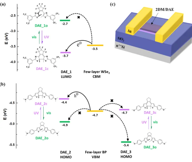
Figure 1. Molecules, energy levels and device structure. (a) and (b) Energy level diagram of
(a) electron transport between WSe2/DAE_1, (b) hole transport between BP/DAE_2 and
BP/DAE_3. Chemical structures of DAE molecules are illustrated as well. Energy level values for DAEs are determined by cyclic voltammetry,[25] for WSe
2 are calculated in the screened
exchange functional[26]
and for BP are calculated based on the HSE06 calculation.[27] (c)
Schematic representation of the 2DM/DAE based FET.
Three DAE derivatives[24-25] displaying different HOMO/LUMO energy levels have
6
requirement to achieve photo-modulation relies on the matching of the energy levels between the host 2DM and DAE molecules, to enable the appearance of trapping states. Likewise when blended with organic semiconductors,[28] the two isomers, DAE_o and DAE_c, feature different
energy levels and can be expected to affect differently the charge transport process through the 2DMs. A schematic illustration of the energy level alignment is depicted in Figure 1a-b. For the intrinsically n-doped WSe2, the energy of the conduction band minimum (CBM) is located
between the LUMO levels of DAE_1o and DAE_1c. In other words, the LUMO of DAE_1o features a higher energy value compared to the CBM of WSe2, thereby impeding the electron
transfer from WSe2 to DAE_1o. Conversely, the DAE_1c isomer behaves as trapping site for
WSe2 electrons, resulting in a decrease of electron density in the FET device. Similarly, for the
BP FET with p-type dominant transport, the BP valance band maximum (VBM) lies energetically between the HOMO levels of DAE_2o and DAE_2c. The driving force for hole trapping therefore exists only in the closed form of DAE_2, leading to a reduced hole density. To further reveal the role of energy levels of DAEs with respect to the tuning of the charge transport in 2DM, we extended our study to BP/DAE_3. With the HOMO of DAE_3c being isoenergetic to the VBM of BP, the photo-triggered hole trapping is nullified.
Conventional back-gated FETs are fabricated with exfoliated 2DM flakes between electrodes and DAE spin-coated on top. Though the electron trapping by DAE is favored by WSe2 with higher CBM level thus thinner thickness, a high electron mobility based on thicker
thickness is essential for achieving multilevel storage with a quantity of distinguishable current levels. The specific thicknesses of the 2DM flakes were chosen in order to ensure a good compromise between the ratio of charge transport modulation and the high device mobility (see Section 3 in the SI).
To evaluate the tendency of DAE to undergo efficient photochemical isomerization when deposited on WSe2, UV-vis absorption spectra of bare WSe2, DAE film and WSe2/DAE
7
films on WSe2 displayed a spectrum which resembles the sum of WSe2 and DAE (Figure S2c,
blue curve), as it combines all their representative bands. Upon UV irradiation, the photochemical isomerization from DAE_1o to DAE_1c occurs, with a spectroscopic behavior being similar to the neat DAE_1 film. The band at 312 nm from DAE_1o clearly diminishes, while the band at 530 nm which originates from DAE_1c appears and superimposes with another band from WSe2 at 520 nm, turning into a broader band (Figure S2c, purple curve). The
initial spectrum can be completely re-established after sequential vis light irradiation. These observations provide clear evidence that the photoisomerization of DAE_1 is not perturbed by the underlying WSe2 surface.
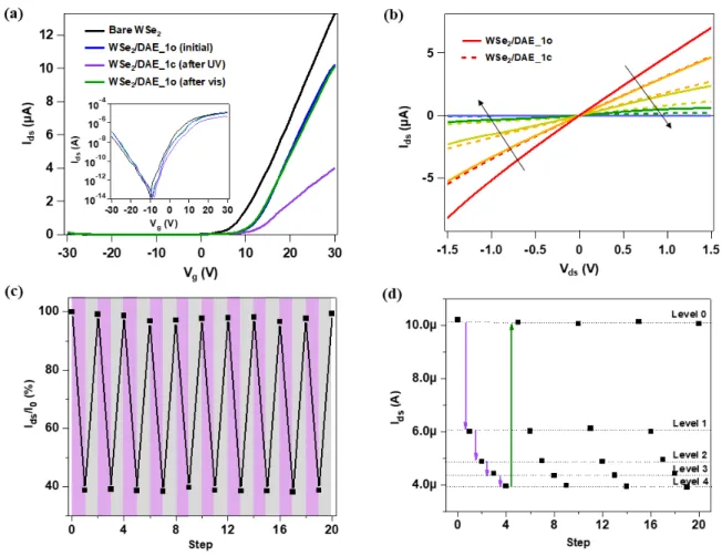
Figure 2. Electrical characterization of WSe2/DAE_1 device. (a) Transfer evolution of bare
WSe2, WSe2/DAE_1 as prepared and after UV/vis irradiation. Inset: the same curves
8
Vg from -30 V to 30 V in steps of 10 V. (c) Ids modulation over 10 illumination cycles with
alternative UV (violet shaded areas) and vis (grey shaded areas) light. All current values are normalized to the initial value obtained from the as prepared WSe2/DAE_1o. The connecting
lines are used as guides to the eye. (d) Multilevel current at fixed illumination times over 4 cycles. All single points of Ids are values recorded from the transfer curve at Vg = 30 V and Vds
= 2 V.
To investigate the effect of the photo-switching of DAE_1 on the charge transport in WSe2 based devices, FETs incorporating a few-layer of mechanically exfoliated WSe2 flakes
have been fabricated and characterized. Initially, the transfer and output characteristics of devices based on bare WSe2 have been measured. Then, the measurement has been repeated
after deposition of the DAE_1o thin film and after UV/vis irradiation. The evolution of the transfer curves is shown in Figure 2a. The device incorporating bare WSe2 exhibited a typical
electron-dominant transport behavior, with a threshold voltage Vth of 7.7 V and electron
mobility μe (extracted from the transfer saturation regime) of 16.6 cm2/V·s (see section 4 in the
SI). The Vth shifts to 8.8 V upon physisorption of the DAE thin film, and the μe decreased to
14.3 cm2/V·s, indicating a minor p-type doping effect on WSe
2. Such an effect is attributed to
the increasing charge scattering centers or trapping states by DAEs. Importantly, such a minor decrease in mobility indicates that upon physisorption of a DAE layer the WSe2 largely
preserves its pristine electrical performance. The conversion from DAE_1o to DAE_1c by UV irradiation for 30 s induced an additional p-type doping. The μe drops from 14.3 cm2/V·s to 5.6
cm2/V·s corresponding to a modulation of 60.8%. On the same time, the V
th is upshifted by 2.5
V, accompanied with a decreasing electron density △ne of 6.25 × 1011 cm-2. As displayed in
Figure 1a, such UV-induced p-doping effect can be ascribed to the fact that the DAE isomerization to the ring-closed form lowered its LUMO energy level by 1.1 eV, corresponding to a level below the CBM of WSe2, allowing the electron donation from the WSe2 to the
9
DAE_1c. Moreover, upon vis light irradiation, the reverse process back to the DAE_1o occurs accompanied with a full recovery of the initial electrical characteristics (Figure 2a, green curve). Such an evidence suggests that the modulation is related to the different photo-isomer states of DAEs, and can be controlled upon alternating irradiation of UV and vis light. Back gate sweeping (from 30 V to -30 V) is also implemented (Figure S5). The obtained transfer curves present a similar evolution as forward gate sweeping, indicating that the transport modulation of WSe2 applies to both forward and backward gate sweeping in spite of the hysteresis. In order
to rule out the possibility that the contribution to the modulation coming from WSe2, it is
mandatory to perform a blank test in which the electrical characteristics of the device based on bare WSe2 without DAEs under the same irradiation conditions are measured. As displayed in
Figure S6a, the device exhibits no sign of photoresponsive behavior. Figure 2b displays the output characteristics of WSe2/DAE_1o and WSe2/DAE_1crespectively. The curves are linear
and symmetrical, confirming the ohmic behavior of WSe2 with respect to Au contact. With
different applied source-drain voltage Vds, source-drain current Ids exhibits a downshift for
DAE_1c modified WSe2 compared to the case of DAE_1o, in analogy with the results of the
transfer measurements.
The electrical characteristics are fully recovered upon vis light irradiation. Subsequently, UV/vis illumination cycles were carried out to investigate the stability of the DAE triggered photoswitching in the hybrid device. Figure 2c plots the normalized Ids at Vg = 30 V and Vds =
2 V over 10 measured illumination cycles. The photoinduced current modulation is calculated to be ca. 61.7 %, showing an efficient electron trapping by DAE_1c. The absence of degradation demonstrates that the light driven current modulation possesses good stability, reversibility, and reproducibility. Detailed transfer curves acquired from these 10 illumination cycles are provided in Figure S7.
In Figure 2d, we present a multilevel current achieved by irradiating the device at different fixed times over 4 cycles. Level 0 is the current state when DAEs are all in their open
10
form, corresponding to the current value obtained at Vg = 30 V in the transfer measurement of
DAE_1o. Level 1 is reached upon 2 s of UV irradiation, and Levels 2, 3 and 4 are obtained by further UV irradiation for 4 s, 8 s and 16 s, respectively. Note that the entire UV irradiation time (30 s) is the same as we used in the former illumination cycles and Level 4 converges to the exact value of Ids when DAEs are all in closed form. We performed 4 switching cycles; the
standard deviation of each level is calculated and then divided by the total current difference between DAE_1o and DAE_1c (Table S1). The value obtained is below 1% for all these 5 levels, indicating that the device can attain a multitude of current levels with a high accuracy readout.
In view of the thermal stability of both photo-isomers, the devices incorporating DAEs are expected to exhibit good retention characteristics. Figure S8 displays the Ids evolution upon
different storage times. The standard derivation for these two levels is calculated respectively and divided by the current difference between DAE_1o and DAE_1c (Ids_1o – Ids_1c, Table
S2). The negligible variation of both current levels after one week, as quantified by a standard deviation below 1.5% of the total current difference, provides unambiguous evidence for the excellent retention capacity of our devices, which renders them interesting elements for potential application as non-volatile memories.[29] Note that here the modulation of Ids is up to
84.6%, and the intrinsic value of electron mobility (1.7 cm2/V·s) is 10 times lower than the
above device (16.6 cm2/V·s). This is because the thickness of WSe2 is thinner, which favors the
electron transfer to DAE_1c and lowers the mobility. The result is consistent with our preliminary prediction.
11
Figure 3. Ids–time measurement under alternative dark and illumination conditions at Vg = 30
V and Vds = 2 V (a) over 16 illumination cycles; (b) an example of one illumination cycle. Each
cycle contains 15 s UV (violet shaded areas) and 2 min vis (grey shaded areas) light. The curve is corrected for bias stress effect.
To further elucidate the effect of DAE photoswitching, the dynamic variation of Ids with
time is measured under alternating dark and illumination conditions, revealing similar trends as in previous experimental observations (Figure 3a). Owing to the bias stress effect when applying a constant positive gate voltage, the Ids decays with time.[30] To address separately the
contribution of DAE photoswitching, the bias-induced decay is fitted and subtracted from the curve (Detailed fitting curve and fitting parameters is provided in Figure S9 and Table S3). Figure 3b displays an example of one switching cycle (each cycle contains 15 s UV ON + 45 s light OFF + 120 s vis ON + 60 s light OFF). The violet boxed regions indicate the period when the UV light is on and the grey boxed regions indicate the period when the vis light is on. The initial current increase upon UV light is due to photocurrent, which can be attributed to the conventional band-to-band transition that generates electron-hole pairs.[31] The Ids then
decreases gradually with time, as a result of the isomerization to DAE_1c, a process accompanied with electron donation from WSe2 to DAE_1c. When UV irradiation is terminated,
12
the decrease in photocurrent leads a rapid drop of Ids owing to the exciton relaxation.[31]
Similarly, for the case of vis illumination, the Ids showed a sudden jump which is the
photoresponse, followed by an increase because of the DAE_1c to DAE_1o back-isomerization. On the OFF state, Ids resumes to the initial value before UV illumination, proving the
modulation of Ids by DAE photoswitching. The absence of fatigue for at least 16 static
illumination cycles demonstrate that the device possesses an excellent stability and endurability. For the sake of comparison, the Ids-time measurement is also performed for the device based on
bare WSe2. As illustrated in Figure S6b and S6c, the device shows only photoresponse, with Ids
ramps upon illumination and suddenly resumes to origin value under dark condition. The blank test unequivocally proves that WSe2 is not responsible for the electron transport modulation
under illumination.
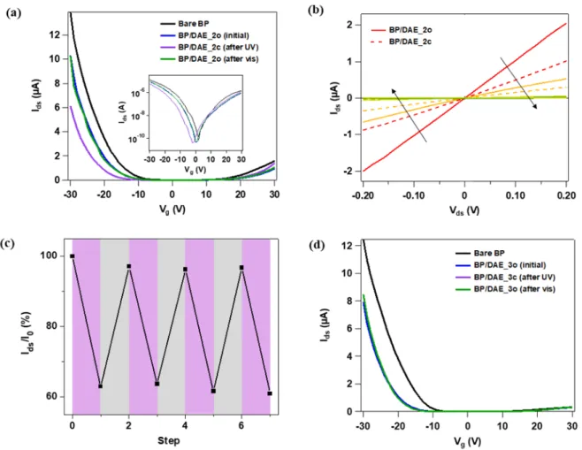
Figure 4. Electrical characterizations of BP/DAE_2 & BP/DAE_3 devices. (a) Transfer
13
curves represented on a logarithmic scale. (b) Output evolution of BP/DAE_2o and BP/DAE_3c for Vg from -30 V to 30 V in steps of 10 V. (c) Normalized Ids modulation over 4
illumination cycles with UV (violet shaded areas) and vis (grey shaded areas) light at Vg = -30
V and Vds = 2V. (d) Transfer evolution of bare BP, BP/DAE_3 as prepared and after UV/vis
irradiation at Vds = 2 V.
To demonstrate the general applicability of the charge transport modulation in two-dimensional semiconductors via energy level phototuning we applied same procedure to BP based FET (Figure 4a). The pristine BP device shows p-type-dominant electrical characteristics with a hole mobility μh = 87.2 cm2/V·s. Upon deposition of the DAE_2o film, the Vth
downshifted and μh decreased to 68.7 cm2/V·s, suggesting that BP is potentially n-type doped
by DAE_2. Subsequent UV irradiation reveals a further decrease of μh by a modulation of
48.9%. The variation is accompanied with a negative shift of Vth by 2.7 V as well as a decrease
of hole density △nh of 6.75 × 1011 cm-2, revealing a further n-type doping effect and a depletion
of the hole carriers. All these variations are recovered back by vis illumination. Such reversible doping effect complies with our picture of hole trapping process: UV irradiation induces the photo-isomerization from DAE_2o to DAE_2c, leading to an increase of corresponding HOMO energy level. The higher HOMO level of DAE_2c act as traps for holes from BP, which is reflected in the decrease of hole density. The vis irradiation converts the photochromic molecules back to ring-open form. The measured output characteristics in Figure 4b shows the same tendency of Ids modulation. The modulation of Ids at Vg = -30 V is around 37.4 % and is
stable over the measured 4 illumination cycles (Detailed transfer curves are provided in Figure S10). Backward gate sweeping is likewise carried out on BP/DAE_2 devices (Figure S11), which shows the same evolution as forward gate sweeping. Reference device with bare BP shows no response by the same light irradiation, therefore the optically induced hole transport modulation can be ascribed to the light-response of the DAE photoswitch (Figure S12).
14
To support above-mentioned interpretation, we have extended our study to BP/DAE_3. Clearly, the Ids decreases after DAE_3 deposition, while no further variation is observed as a
result of either UV or vis light irradiation. Taking into account the energy levels depicted in Figure 1b, the result is not surprising because of the absence of driving force for hole transfer from BP to DAE_3c. This phenomenon provides clear evidence that suitably designed DAEs possessing ad hoc energy level alignment with the semiconducting 2DMs is required to achieve efficient optical modulation of the charge transport in the hybrid devices.
In summary, we have fabricated two-dimensional semiconductor-based light-responsive FETs via energy level phototuning. The device’s electrical performance can be reversibly modulated by light illumination with well-defined wavelengths. In particular, the physisorbed photochromic DAEs act as optical switching elements, thereby allowing for the fine-tuning and remote control over the charge transport of the host 2DM. To prove the general applicability of our approach we have challenged it by realizing n- and p-type dominated ambipolar FETs containing a few-layer WSe2 and BP, respectively. In each pair of 2DM/DAE, the modulation
is achieved when the CBM or VBM of 2DM is energetically sandwiched between the LUMO or HOMO gap of the two photo-isomers of DAEs, respectively. Our approach is thus proved feasible for both electron and hole transport modulation depending on the nature of target 2DM without sacrificing their intrinsic performance, confirming its general applicability and effectiveness. Our strategy can be extended to modulate the electrical characteristics of devices integrating other 2DMs by simply choosing suitable DAEs, thereby opening the door for multi-responsive 2DM/DAEs based FETs that can be switched ON and OFF upon irradiation with light. Noteworthy, the FET device based on such 2DM/DAE system displayed excellent data retention capacity and a high accuracy readout with several distinguishable current levels, opening perspectives towards their use as multilevel non-volatile memory. Furthermore, such controlled optical switching of the charge injection and transport in 2DM-based systems may pave the way to a new era of electronics, which incorporate novel functions in a single device
15 based on high-performing 2D materials.
Experimental Section
Experimental details are available in the Supporting Information.
Supporting Information
Supporting Information is available from the Wiley Online Library or from the author.
Acknowledgements
We acknowledge funding from the European Commission through the Graphene Flagship Core 2 project 785219), the Marie Sklodowska-Curie projects ITN project iSwitch (GA-642196), the Marie-Curie IEF STELLAR (GA-795615), the M-ERA.NET project MODIGLIANI, the European Research Council (ERC via ERC-2012-STG_308117 “Light4Function”), the Agence Nationale de la Recherche through the Labex projects CSC (ANR-10-LABX-0026 CSC) and NIE (ANR-11-LABX-0058 NIE) within the Investissement d’Avenir program (ANR-10-120 IDEX-0002-02), the International Center for Frontier Research in Chemistry (icFRC), the German Research Foundation (DFG via SFB 658, project B8) as well as the Chinese Scholarship Council.
Received: ((will be filled in by the editorial staff)) Revised: ((will be filled in by the editorial staff)) Published online: ((will be filled in by the editorial staff))
References
[1] A. C. Ferrari, F. Bonaccorso, V. Fal'ko, K. S. Novoselov, S. Roche, P. Bøggild, S. Borini, F. H. L. Koppens, V. Palermo, N. Pugno, J. A. Garrido, R. Sordan, A. Bianco, L. Ballerini, M. Prato, E. Lidorikis, J. Kivioja, C. Marinelli, T. Ryhänen, A. Morpurgo, J. N. Coleman, V. Nicolosi, L. Colombo, A. Fert, M. Garcia-Hernandez, A. Bachtold, G. F. Schneider, F. Guinea, C. Dekker, M. Barbone, Z. Sun, C. Galiotis, A. N. Grigorenko, G. Konstantatos, A. Kis, M. Katsnelson, L. Vandersypen, A. Loiseau, V. Morandi, D.
16
Neumaier, E. Treossi, V. Pellegrini, M. Polini, A. Tredicucci, G. M. Williams, B. Hee Hong, J.-H. Ahn, J. Min Kim, H. Zirath, B. J. Van Wees, H. Van Der Zant, L. Occhipinti, A. Di Matteo, I. A. Kinloch, T. Seyller, E. Quesnel, X. Feng, K. Teo, N. Rupesinghe, P. Hakonen, S. R. T. Neil, Q. Tannock, T. Löfwander, J. Kinaret, Nanoscale 2015, 7, 4598. [2] F. Bonaccorso, Z. Sun, T. Hasan, A. C. Ferrari, Nat. Photonics 2010, 4, 611.
[3] Q. H. Wang, K. Kalantar-Zadeh, A. Kis, J. N. Coleman, M. S. Strano, Nat. Nanotechnol.
2012, 7, 699.
[4] F. Xia, H. Wang, D. Xiao, M. Dubey, A. Ramasubramaniam, Nat. Photonics 2014, 8, 899.
[5] F. Bonaccorso, L. Colombo, G. Yu, M. Stoller, V. Tozzini, A. C. Ferrari, R. S. Ruoff, V. Pellegrini, Science 2015, 347, 1246501.
[6] L. Dai, Acc. Chem. Res. 2012, 46, 31.
[7] H.-J. Choi, S.-M. Jung, J.-M. Seo, D. W. Chang, L. Dai, J.-B. Baek, Nano Energy 2012, 1, 534.
[8] W. Wu, L. Wang, Y. Li, F. Zhang, L. Lin, S. Niu, D. Chenet, X. Zhang, Y. Hao, T. F. Heinz, J. Hone, Z. L. Wang, Nature 2014, 514, 470.
[9] S. Bertolazzi, M. Gobbi, Y. Zhao, C. Backes, P. Samorì, Chem. Soc. Rev. 2018, 47, 6845.
[10] C. Anichini, W. Czepa, D. Pakulski, A. Aliprandi, A. Ciesielski, P. Samorì, Chem. Soc. Rev. 2018, 47, 4860.
[11] Q. He, S. Wu, Z. Yin, H. Zhang, Chem. Sci. 2012, 3, 1764. [12] S. Wu, Q. He, C. Tan, Y. Wang, H. Zhang, Small 2013, 9, 1160.
[13] Y. Zhao, S. Ippolito, P. Samorì, Adv. Opt. Mater. 2019 in press (DOI: 10.1002/adom.201900286).
[14] M. Gobbi, E. Orgiu, P. Samorì, Adv. Mater. 2018, 30, 1706103. [15] E. Orgiu, P. Samorì, Adv. Mater. 2014, 26, 1827.
17
[16] X. Zhang, L. Hou, P. Samorì, Nat. Commun. 2016, 7, 11118. [17] H. M. D. Bandara, S. C. Burdette, Chem. Soc. Rev. 2012, 41, 1809. [18] R. Klajn, Chem. Soc. Rev. 2014, 43, 148.
[19] M. Irie, T. Fukaminato, K. Matsuda, S. Kobatake, Chem. Rev. 2014, 114, 12174. [20] Y. Zhao, S. Bertolazzi, P. Samorì, ACS Nano 2019, 13, 4814.
[21] M. Kim, N. S. Safron, C. Huang, M. S. Arnold, P. Gopalan, Nano Lett. 2012, 12, 182. [22] M. Gobbi, S. Bonacchi, J. X. Lian, A. Vercouter, S. Bertolazzi, B. Zyska, M. Timpel,
R. Tatti, Y. Olivier, S. Hecht, M. V. Nardi, D. Beljonne, E. Orgiu, P. Samorì, Nat. Commun. 2018, 9, 2661.
[23] A. R. Jang, E. K. Jeon, D. Kang, G. Kim, B.-S. Kim, D. J. Kang, H. S. Shin, ACS Nano
2012, 6, 9207.
[24] M. Herder, F. Eisenreich, A. Bonasera, A. Grafl, L. Grubert, M. Pätzel, J. Schwarz, S. Hecht, Chem. Eur. J. 2017, 23, 3743.
[25] M. Herder, B. M. Schmidt, L. Grubert, M. Pätzel, J. Schwarz, S. Hecht, J. Am. Chem. Soc. 2015, 137, 2738.
[26] Y. Guo, J. J. Robertson, Appl. Phys. Lett. 2016, 108, 233104. [27] Y. Cai, G. Zhang, Y.-W. Zhang, Sci. Rep. 2014, 4, 6677.
[28] E. Orgiu, N. Crivillers, M. Herder, L. Grubert, M. Pätzel, J. Frisch, E. Pavlica, D. T. Duong, G. Bratina, A. Salleo, N. Koch, S. Hecht, P. Samorì, Nat. Chem. 2012, 4, 675. [29] S. Bertolazzi, P. Bondavalli, S. Roche, T. San, S.-Y. Choi, L. Colombo, F. Bonaccorso,
P. Samorì, Adv. Mater. 2019, 31, 1806663.
[30] K. Cho, W. Park, J. Park, H. Jeong, J. Jang, T.-Y. Kim, W.-K. Hong, S. Hong, T. Lee, ACS Nano 2013, 7, 7751.
[31] Y.-C. Wu, C.-H. Liu, S.-Y. Chen, F.-Y. Shih, P.-H. Ho, C.-W. Chen, C.-T. Liang, W.-H. Wang, Sci. Rep. 2015, 5, 11472.