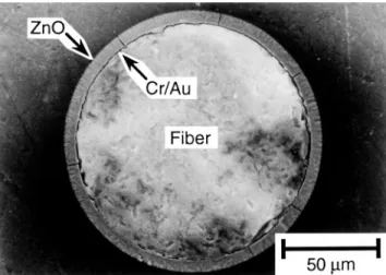
Fabrication and structural analysis of ZnO coated fiber optic
phase modulators
G. R. Fox and N. Setter
Ecole Polytechnique F´ed´erale de Lausanne, Laboratoire de C´eramique, Lausanne, Switzerland, CH-1015
H. G. Limberger
Ecole Polytechnique F´ed´erale de Lausanne, Laboratoire d’Optique Appliqu´ee, Lausanne, Switzerland, CH-1015
(Received 17 March 1995; accepted 1 December 1995)
Fiber optic modulators were fabricated by coating optical fibers with electrode and piezoelectric ZnO layers. The techniques of piezoelectric fiber optic modulator (PFOM) fabrication are presented, and the microstructure and crystallographic texture of the coatings are analyzed. In order to produce thick (approximately 5 mm) ZnO coatings, it was necessary to study the reactive dc magnetron sputtering process in O2yAr gas mixtures under conditions close to the transition between an oxidized and nonoxidized Zn target surface. In situ quartz crystal microbalance measurements of the deposition rate revealed thee distinct regions in the deposition rate (R) vs oxygen partial pressure (PO2) behavior, at constant total pressure, for sputtering under conditions that provided an oxidized Zn target surface. Additionally, a transition between oxygen and argon dominated sputtering as observed by varying the sputtering pressure while maintaining a constant PO2. The transition between oxygen and argon dominated sputtering influences
R to varying extents within the three R vs PO2 regions for an oxidized target surface. Correlations among the cathode current and voltage, deposition rate, and gas flow rate are presented to give a better understanding of the reactive sputtering processes occurring at the oxidized Zn target surface. Sputtering conditions optimized for a high ZnO deposition rate were used to producek001l radially oriented ZnO fiber coatings for PFOM devices that can produce optical phase shifts as large as 0.38 radyV.
I. INTRODUCTION
Piezoelectric coatings on optical fibers provide a method for modulating the strain within a section of fiber. Straining a fiber changes the fiber dimensions as well as the fiber refractive index, due to the photoelastic effect. Modulation of the fiber length and refractive index can be used to induce a phase modulation in an optical signal passing through the fiber.1–4Besides phase shifter and modulator applications, piezoelectric coated optical fibers can also be exploited in electric field sens-ing devices.5–7 Polymer1–4,8,9 and ZnO10–12 piezoelectric coatings on optical fibers have been investigated for phase modulation applications. Sputter deposited axially symmetric ZnO coatings provide several advantages for piezoelectric fiber optic modulator (PFOM) fabrication and operation in comparison with polymer coatings.13–15 Since the optical fiber is used as the substrate for the deposition of ZnO, the centering problem associated with the fabrication of polymer coatings is eliminated. Thin coatings (on the order of 1 mm) of ZnO may reduce the driving voltage requirements for a modulator, and the acoustic coupling may be improved due to a better matching of the elastic properties between the ZnO and the fiber substrate.
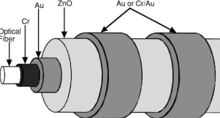
This paper presents a description of the coating and masking methods used for fabrication of ZnO-based PFOM devices with the axially symmetric structure shown in Fig. 1. Preparation of PFOM devices required the development of fiber cleaning methods to assure the adhesion of fiber coatings. Additionally, it was necessary to optimize the reactive dc magnetron sputtering process to obtain high ZnO deposition rates for the production of coatings with thicknesses of up to 6 mm. Deposition of ZnO by reactive sputtering from a Zn target has been
FIG. 1. Diagram of a piezoelectric fiber optic modulator (PFOM) that uses axially symmetric electrode and ZnO coatings.
studied by a number of authors.16–20It is well established that the sputtering process exhibits a transition between the metal and oxide mode at some critical oxygen partial pressure, PO2 Pc.
21 Above P
c, oxygen ions
and molecules cause the formation of a surface oxide layer on the target, which reduces the sputtering rate of the Zn target and causes oxidized species of Zn to be ejected. Below Pc, the fluence of oxygen species
incident on the surface of the target is not sufficient to form an oxide coating, and reduced Zn species are ejected. At the transition between the metal (PO2 , Pc)
and oxide (PO2. Pc) sputtering modes, a sharp decrease
in the sputtering rate is observed. The sputtering rate is reduced because of dilution of the Zn atoms with oxygen and because the surface binding energy of Zn in ZnO is higher than in the metal.22,23 A hysteresis, due to differences in the Zn sputtering rate and corre-sponding reaction kinetics at the target surface, occurs when cycling through the transition by increasing and decreasing PO2.
24 In order to determine the maximum deposition rates attainable in the oxide sputtering mode (PO2 . Pc), in situ measurements of the deposition rate were made as a function of P, PO2, and applied cathode power (PW). In particular, experiments focused on the region close to the transition. The enhanced deposition rates found for sputtering conditions close to Pc, but still
within the oxide sputtering mode, were used to obtain ZnO coatings on CryAu coated optical fibers for PFOM devices.
For the analysis of PFOM devices, an emphasis was placed on establishing standard x-ray diffraction (XRD) methods for the crystal structure and texture characterization of coatings on fiber substrates. Since fibers provide a very small surface area for analysis,
x-ray diffractometer methods cannot be easily applied. Analysis with a Debye – Scherrer diffraction camera was found to be ideal since this method requires a fiber sample. Diffraction analysis along with SEM observa-tions were used to determine the structure of ZnO-based PFOM devices.
II. EXPERIMENTAL PROCEDURE
A. Fiber cleaning and electrode deposition
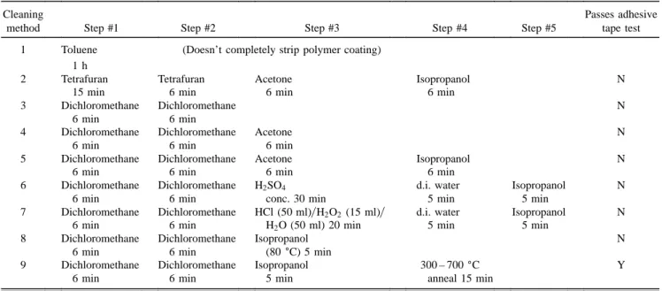
Two types of 125 mm diameter fibers with 9 mm diameter cores were used as substrates for PFOM fab-rication. One type of fiber was a standard telecommu-nication fiber, and the other was a high strength fiber that contained an extra 4 mm thick Ti-doped over-cladding layer.25 Both fiber types were received with a double layer polymer coating that protects the fiber under normal use. A 6 min soak in dichloromethane26 in an ultrasonic cleaner was used to dissolve the inner polymer coating and allow easy stripping of the outer polymer layer. After stripping the protective coating, the surface of the standard fiber could be sufficiently cleaned by using sequential 6 min ultrasonic washes in dichloromethane, acetone,27and 2-propanol.28Several surface cleaning methods were tested for the Ti-doped over-cladded fibers, as listed in Table I. A cleaning process was considered to be acceptable if a CryAu coat-ing exhibited sufficient adhesion to pass the commonly used adhesive tape29 test.30
The stripped and cleaned fibers, approximately 19 cm long, were mounted into stainless steal fiber chucks using a polymer cement.31 Up to five mounted fibers were loaded into the stainless steel rotating fiber TABLE I. Cleaning methods studied for improving adhesion of CryAu coatings on high strength Ti-doped over-cladded fibers.
Cleaning Passes adhesive
method Step #1 Step #2 Step #3 Step #4 Step #5 tape test
1 Toluene (Doesn’t completely strip polymer coating)
1 h
2 Tetrafuran Tetrafuran Acetone Isopropanol N
15 min 6 min 6 min 6 min
3 Dichloromethane Dichloromethane N
6 min 6 min
4 Dichloromethane Dichloromethane Acetone N
6 min 6 min 6 min
5 Dichloromethane Dichloromethane Acetone Isopropanol N
6 min 6 min 6 min 6 min
6 Dichloromethane Dichloromethane H2SO4 d.i. water Isopropanol N
6 min 6 min conc. 30 min 5 min 5 min
7 Dichloromethane Dichloromethane HCl (50 ml)yH2O2 (15 ml)y d.i. water Isopropanol N
6 min 6 min H2O (50 ml) 20 min 5 min 5 min
8 Dichloromethane Dichloromethane Isopropanol N
6 min 6 min (80±C) 5 min
9 Dichloromethane Dichloromethane Isopropanol 300 – 700±C Y
holder shown in Fig. 2. A gear drive assembly at one end of the fiber holder provides for rotation of each fiber.
To deposit bottom electrode layers of Cr and Au onto the fibers, the fiber holder was mounted horizontally 15.5 cm above the metal charge inside a resistance heated thermal evaporation system.32 A variable speed motor driven rotary feedthrough drove the rotating fiber holder during the deposition process. The deposition rate (R) and thickness (l) of the evaporated coatings were monitored with a quartz crystal microbalance33 (QCM). For PFOM fabrication, a Cr layer 13 nm thick and Au layer 130 nm thick were deposited at rates of 1 and 10 nmymin (this is the deposition rate onto the fiber as opposed to the equivalent flat substrate deposition rate, which is a factor of p larger), respectively, while the fibers were rotated at a rate of 2 rpm. Cr coated W rods34and Au wire35placed in a Mo boat36were used for the evaporation sources. The pressure during evaporation was 1 ? 1024 Pa. To facilitate splicing of the PFOM into a fiber optic circuit, the ends of the fibers were masked by aluminum plates that were attached to the ends of the fiber holder. The masking method resulted in fibers with 10 cm long CryAu bottom electrode coatings and 4 to 5 cm uncoated ends.
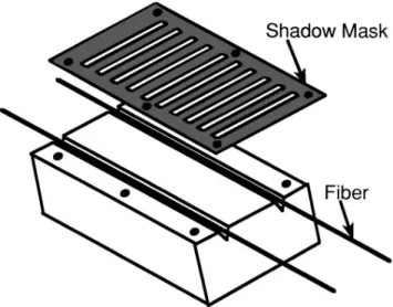
Top electrode bands of CryAu and Au layers were deposited onto CryAuyZnO coated fibers using a shadow mask, as shown in Fig. 3. The shadow mask was mounted on the fiber holder such that the fibers in the top two positions were aligned to allow rotation behind the mask. Three types of electrodes were studied: 130 nm Au (R 10 nmymin), 400 nm Au (R 30 nmymin), and 25 nm Cr (R 2.5 nmymin)y400 nm Au (R 30 nmymin). Electrode lengths of 2 and 6 mm, separated by 2 mm spaces, were deposited over 8 cm sections of CryAuyZnO coated fibers while using a fiber rotation speed of 2 rpm.
B. ZnO deposition
ZnO was deposited by reactive dc magnetron sput-tering from a 10 cm diameter Zn target37 in a mixed atmosphere of O2and Ar. The vacuum system consisted of a diffusion pump38 backed by a rotary mechanical
FIG. 2. Diagram of rotating holder used for rotating fibers during evaporation and sputter deposition of electrode and ZnO coatings.
FIG. 3. Shadow mask used in combination with the rotating fiber holder to structure PFOM top electrode coatings.
pump39 that could produce a base chamber pressure of 1 ? 1025 Pa. A variable position gate valve40 made it possible to precisely adjust the opening to the diffusion pump. Flow rates for O2 and Ar were controlled with a set of mass flow controllers.41 Pressure was monitored using a capacitance manometer42 with a pressure reso-lution of 1 ? 1025Pa and rating for a maximum pressure of 10 Pa. Power was supplied to the magnetron source43 using a dc power supply44 with a maximum output of 1 kV and 1 A. The power supply was operated in the power mode, which maintained constant power by automatically adjusting cathode voltage. The deposited mass and mass deposition rate were measured using a QCM45 interfaced with a computer. Deposition rate was determined from a linear regression of 5 mass measurements taken at 2 s intervals.
Before depositing ZnO coatings on fibers, the dc reactive sputtering of Zn was studied by observing the QCM measured deposition rate and cathode current (Ic) and voltage (Vc) as a function of P and PO2 at constant cathode power, PW. The target was first presputtered in pure oxygen until a steady-state deposition rate was obtained. To measure the deposition rate change with PO2 at constant P, the flow rate of the oxygen was decreased in steps to lower the PO2, while the Ar flow rate was increased to maintain constant pressure; the gate valve was placed in a fixed position to maintain a constant pumping speed (S). A steady-state deposition rate was obtained at each P and PO2condition, and the deposition rate was determined by averaging the rate measured over a 6 min period. The deposition rate measurements as a function of P at constant PO2were made using a similar procedure, but in this case, the oxygen flow rate was held constant while the Ar flow rate was adjusted to increase P. It should be noted that this procedure, since
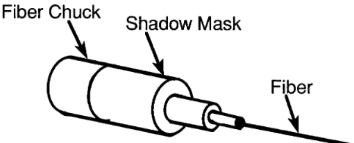
it consists of incremental changes in PO2or P, allows the measurement of PO2 and P during discharge. The size of the pressure increments must be chosen with caution since the measurement errors are additive on moving away from the initial sputtering conditions. All the deposition rate measurements were made with a target to substrate distance, D, of 16.4 cm, and while sputtering in the oxide mode; i.e., the target maintained an oxide surface. After choosing the conditions for deposition of ZnO coatings, the spatial distributions of the deposited ZnO, for target distances of D 8.8 and 16.4 cm, were determined by using a profilometer46 to measure the thickness of films deposited onto masked Si wafers.47 ZnO coatings for PFOM devices were deposited under steady-state deposition conditions using an applied dc power of 250 W, P 1.50 Pa, PO2 0.70 Pa, and fiber rotation rate of 5.6 rpm. Coatings deposited with D 8.8 and 16.4 cm were investigated. During deposition of the ZnO onto CryAu coated fibers, a set of masks were attached to the fiber mounting chucks (Fig. 4) to block deposition at the mounted end of each fiber. The masked end provided an exposed section for electrical contact with the bottom electrode and also maintained a section of uncoated fiber for splicing. After each sputtering run, the Zn target was ground with 320 grit SiC paper to remove cones that formed on the target surface; surface grinding reduces the problem of arcing during sputtering. The target was washed with 2-propanol to remove loose particles of Zn and SiC.
C. Fiber coating analysis
The crystal structure and texture of the deposited coatings were determined by x-ray diffraction using Ni filtered Cu Ka (40 kV and 35 mA) radiation and a 114.6 mm diameter Debye – Scherrer camera with a 0.5 mm diameter aperture.48 This method is ideal for investigating the crystallographic structure of fiber coat-ings since it requires a fiber or wire specimen. Approx-imately 1 cm segments of coated fibers were placed in the camera, and single emulsion films49 were exposed for 5 h. Intensity vs 2u and d plots were obtained by analyzing the films with an optical densitometer.50
FIG. 4. Diagram of a shadow mask that is attached to the fiber chuck of the rotating fiber holder during sputter deposition of ZnO.
Micrographs of the fiber coatings were obtained by scanning electron microscopy51,52Cross-section sam-ples were prepared by mounting the fibers in resin53 and polishing a cross-section surface with a series of SiC paper and diamond paste grades culminating with 0.25 mm abrasive. During polishing, 2-propanol was used as a wetting agent. Samples for observations of the fiber coating surfaces and fracture cross sections were prepared by directly mounting sections of fiber on a metal stud using carbon or silver paint. The polished cross-section samples were sputter coated with Au, but fracture cross-section samples and samples for surface analysis were observed without applying a Au coating.
III. RESULTS AND DISCUSSION
A. Fiber cleaning, CryyyAu adhesion, and bottom electrode structure
Well adhering evaporated CryAu electrodes were ob-tained on standard telecommunication fiber by cleaning in dichloromethane, acetone, and 2-propanol. With Ti-doped over-cladded fibers, the same cleaning procedure resulted in poorly adhering CryAu coatings that peeled away from the fiber surface over extended time periods. Because of the observed adhesion problems, the cleaning procedures listed in Table I were investigated for the Ti-doped over-cladded fibers. Only cleaning procedures that incorporated an annealing step after the final chemi-cal rinse showed any significant improvement in the adhesion of CryAu films. Annealing the Ti-doped over-cladded fibers at temperatures above 300±C for 15 min in air resulted in CryAu coated fibers that passed the adhesive tape test. From the cleaning tests, it can be concluded that the Ti-doped over-cladded fibers adsorb chemical residues that can be removed only by heat treatment and which affect the adhesion of evaporated CryAu if they are not removed from the fiber surface. In comparison, the surface of standard telecommunication fiber must be less favorable for adsorption of residues, or adsorbed residues are more easily removed and leave the surface when the fibers are placed in vacuum for the evaporation process. Procedure number 9 in Table I, with an annealing temperature of 400±C, was followed to ensure the formation of well adhering CryAu coatings for PFOM device fabrication on Ti-doped over-cladded fibers.
An SEM cross-section image of the CryAu bottom electrode layer of a PFOM is shown in Fig. 5. The CryAu coatings are continuous with a smooth fiber interface. Surface images reveal a polycrystalline Au structure of approximately 20 nm diameter grains. Debye – Scherrer XRD of Au coated fibers produces the typical face-centered-cubic pattern for Au. The uniformity and the relative intensities of the rings in the XRD pattern indicate a randomly oriented polycrystalline structure,
FIG. 5. SEM image of a PFOM polished cross section showing the uniform CryAu bottom electrode coating.
but some radial textures, such as k111l (a commonly observed preferred orientation for Au deposited on flat substrates),54could produce a similar diffraction pattern. By comparing simultaneous depositions that were made on Si wafers and on fibers, it is found that the Cr and Au deposition rate on a fiber is a factor 1yp lower than on a wafer. This difference in deposition rate is expected since evaporation is a line-of-sight process and the fibers are rotated during deposition, resulting in an increase in substrate surface area by a factor p. Thickness distributions measured on Si substrates indicate a parabolic decrease in thickness with respect to the position directly above the evaporation source. The following equations give the percent deviation in Cr and Au thickness with distance (in mm) from the deposition maximum: jCr 1.46 ? 1022x 2 5.84 ? 1023x2, jAu 1.63 ? 1022x 27.60 ? 1023x2. The distributions exhibit a thickness variation of less than 15% for an 8 cm diameter area centered above the source. It is expected that similar thickness distributions occur on an 8 cm length of fiber but with an accompanying reduction in total thickness by the factor 1yp.
B. ZnO reactive sputtering and fiber coating deposition
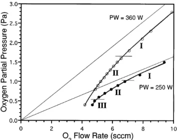
In order to determine the conditions required for depositing ZnO fiber coatings up to 6 mm thick, the reactive sputtering process was studied in the oxide mode, approaching Pcfrom high PO2. Figure 6 shows the deposition rate as a function of decreasing PO2 for two different sputtering conditions. For an applied power of 250 W, three regions (at least one is linear) are observed, and at 360 W two linear regions are observed. Powers higher than 360 W could not be attained due to the current limitations of the dc power supply. The PO2 below which the oxide mode could not be maintained is indicated by the shaded region. Changes in the slope
FIG. 6. ZnO deposition rate dependence on decreasing PO2 toward the transition (Pc) between oxide and metal sputtering modes. Distinct
linear R vs PO2 regions are observed for two different sputtering conditions: PW 250 and P 1.50 Pa; PW 360 W and P 2.80 Pa.
between the various R vs PO2 regions correspond to changes in the behavior of PO2 vs flow rate (Fig. 7) and the cathode current and voltage dependence on PO2 (Fig. 8).
In region I, the lowest deposition rates are observed, and only a gradual increase in deposition rate occurs with decreasing PO2. The relatively high PO2 (PO2 is well above Pc) ensures a stable oxide surface on the
metal target. Since argon ions have a higher atomic mass than oxygen ions, the slope in region I may be associated with the change in sputtering efficiency that
FIG. 7. Dependence of the PO2on O2flow rate for Zn sputtering with PW 250 W at P 1.50 Pa and PW 360 W at P 2.80 Pa. The nonlinear behavior in regions II and III indicates a change in the gettering rate as Pc is approached. The straight lines in the plot
FIG. 8. Variation of the ZnO cathode current and voltage with de-creasing PO2 approaching Pc for PW 250 W and a fixed P 1.50 Pa.
would accompany an increase in the average atomic mass of the sputtering ions. A nearly constant gettering rate of O2 occurs in region I since the PO2 exhibits a nearly linear dependence on O2 flow rate (Fig. 7), and the linear behavior exhibits a slope that corresponds to that observed for no applied power (straight lines in Fig. 7).55,56 A decrease in current and corresponding increase in voltage accompanies the decreasing PO2 in region I (Fig. 8). Since the current and voltage behavior of the cathode is a complex function of the target surface condition, ion bombardment, and secondary electron and ion emission, a complete explanation of this behavior cannot be given from these results. The current and voltage behavior are given solely to show the correlation between the variables used to control the sputtering process.
Region II also exhibits a linear R vs PO2 behavior (Fig. 6), but the deposition rate increases more rapidly with decreasing PO2than in region I. The PO2 vs O2flow rate curves show a significant deviation from linearity in region II (Fig. 7); this indicates that the gettering rate of O2increases with decreasing PO2. In contrast to region I, an increase in cathode current and a decrease in voltage is observed in region II (Fig. 8). These observations for region II suggest that oxide coverage on the surface of the target decreases (either in thickness or area) as PO2 is decreased. The transition between region I and II may be explained by considering the volume of oxide formed on the target surface. Below some critical oxide layer thickness, bombarding ions with sufficiently high momentum will cause ejection of the oxidized surface atoms and the underlying metal atoms in the reduced state. Fractional oxide coverage of the target surface will also result in the ejection of a mixture of oxidized and reduced species. As the volume fraction of oxide surface is decreased, the number of sputtered metal species is expected to increase relative to the number of sputtered
oxygen containing species; therefore, the sputtering rate will increase toward the rate observed for the pure metal as PO2 decreases. With an increase in sputtered metal species, an increase in the O2 gettering rate results from the increased exposure of unoxidized metal surface at the target, and the fraction of unoxidized metal content in the deposited material may increase.24,57,58
Region III is observed only at the lower target power, and deposition under these conditions cannot be maintained for time periods longer than approximately 30 min. This may be a metastable region that depends on the oxide surface coverage formed during presput-tering and while obtaining measurements at high PO2. More detailed work in this region is needed before a mechanism for the dependence of the deposition rate on PO2 can be proposed.
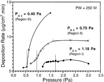
As shown in Fig. 9, the pressure dependence of the deposition rate at constant PO2varies significantly for the three R vs PO2 regions observed for an applied power of 250 W. In region I (PO2 1.18 Pa), R shows only a small dependence on P; R is nearly constant between 1.3 and 3.0 Pa. In region II (PO2 0.70 Pa), R increases with
P up to P 1.6 Pa, where a plateau is reached. Region III also exhibits a large increase in deposition rate with pressure, but a plateau region is not observed because the oxide sputtering mode could not be maintained at pres-sures above 1.50 Pa. The gettering rate remains constant over the entire pressure range (P vs Ar plus O2flow rate is linear with a slope that corresponds to the slope ob-served at no applied power) for all three PO2 conditions, indicating that the rate of oxidation at the target and in the sputtered material remains constant over the entire pressure range. Since the gettering rate of O2is constant as a function of P, mechanisms other than changes in
FIG. 9. ZnO deposition rate dependence on total chamber pressure for constant PO2 0.40, 0.70, and 1.18 Pa and PW 250 W. Each curve exhibits an inflection point at the fractional Ar pressure, FAr 0.28.
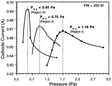
the rate of oxidation at the target surface and in the sputtered material must be responsible for the changes in the deposition rate. Both ionization efficiency and speciation of the bombarding ions, i.e., argon vs oxygen ions, are likely to play an important role in the observed R vs P behavior. Each R vs P curve (Fig. 9) exhibits an inflection point that coincides with a maximum in the cathode current vs pressure behavior (and corresponding minimum in the cathode voltage vs pressure behavior) shown in Fig. 10. The cathode current maximum occurs at the same fractional gas content FAr PAry(PO2 1
PAr) 0.28 6 0.03 for each of the three curves. Both the peaks in the cathode current and the corresponding inflection points in the R vs P curves suggest that a transition occurs between oxygen dominated sputtering and Ar dominated sputtering at FAr 0.28. In the R vs PO2 region I, the change from Ar dominated sputtering (FAr . 0.28) to oxygen dominated sputtering (FAr , 0.28) has little effect on the deposition rate, but in regions II and III, R is greatly enhanced by changing from Ar to oxygen dominated sputtering (Fig. 9).
From the above analysis of the deposition rate dependence on PO2 and P, it is found that significant increases in the deposition rate of ZnO can be obtained by working in region II, which exhibits a stable oxi-dized target surface but a linearly variable deposition rate. Within region II additional enhancements of the deposition rate can be obtained by working with FAr . 0.28. The observed behavior in R vs PO2 in region II, which is most likely to result from changes in the target oxide surface layer, also suggests that it may be possible to alter the relative quantities of oxidized Zn sputtered from the target and therefore change the quantity of Zn that oxidizes at the substrate.
FIG. 10. Zn cathode current dependence on pressure for PO2 0.40, 0.70, and 1.18 Pa and PW 250 W. Each curve exhibits a maximum at the fractional Ar pressure, FAr 0.28.
In order to obtain high deposition rates of ZnO while maintaining stable sputtering conditions over time periods of several hours, the following conditions were chosen for deposition of ZnO fiber coatings: P1.50 Pa, PO2 0.70 Pa, and PW 250 W. These conditions fall within region II of the R vs PO2 curve and FAr 0.53. Cone formation on the Zn target surface, which resulted in arcing, limited deposition times to 3 to 4 h. Since the deposition time was limited, the thicknesses of fiber coat-ings produced at D 8.8 and 16.4 cm were limited to a maximum of 7 and 3 mm, respectively. Cathode powers higher than 250 W increased the probability of arcing and significantly reduced the stable deposition time.
Thickness profiles, for depositions on Si wafers with D 8.8 and 16.4 cm, exhibited a parabolic distribution. The radius of curvature increased with de-creasing target to substrate distance as shown by the following equations, which give the percent thickness deviation as a function of distance (in mm) from the ZnO thickness maximum: j(D 8.8 cm) 2 0.108x 2 1.11 ? 1022x2 and j(D 16.4 cm) 3.69 ? 1022x 2 8.14 ? 1023x2. For D 8.8 cm, which was utilized for making PFOM devices with ZnO coatings up to 6 mm thick, the thickness decreases by less than 25% for a radial distance of 4 cm from the deposition maximum. Depositions made with D 16.4 cm resulted in a thickness deviation of less than 15% at a radial distance of 4 cm. The thickness distributions are expected to be similar for depositions on fibers, but in comparison with the thickness of coatings deposited on flat substrates, some reduction is expected due to the factor of p difference in the surface areas. It was observed that fiber coating thicknesses were thinner than coatings on flat substrates by a factor of 0.71. This is significantly larger than the 1yp factor difference observed for Cr and Au fiber coatings prepared by evaporation; therefore, sputter deposited ZnO oxide coatings are more uniformly distributed on the fiber surface than evaporated electrode coatings. Since scattering events occur under the pressure conditions used for sputtering, the deposition of ZnO is not a line of sight process.59 Additionally, the cathode is large in comparison to the fiber substrates. Both scattering and the size disparity between the cathode and the fibers cause material to be deposited more uniformly over the surface of the fiber than for a simple normal incidence (as obtained for deposition by evaporation) of the depositing material.
C. Analysis of ZnO layer and top electrodes
ZnO coatings deposited on CryAu coated fibers using D 8.8 and 16.4 cm were axially symmetric (Fig. 11) and exhibited uniform surfaces (Fig. 12) over fiber lengths of 8 cm. According to SEM and XRD analysis, there were no differences between the coatings
FIG. 11. SEM image of a PFOM polished cross section showing the radial uniformity of CryAuyZnO coatings.
FIG. 12. SEM image showing the length uniformity of a CryAuyZnO coating.
deposited at D 8.8 and 16.4 cm other than the maximum attainable thickness and surface roughness, which scales with thickness. The ZnO microstructure consisted of columnar grains that were oriented along the radius of the fiber (Fig. 13). Films between 5 and 6 mm thick exhibited a smooth interface at the CryAu bottom electrode (Fig. 5), but the top surface exhibited a roughness of approximately 0.3– 0.5 mm with grain diameters of approximately 0.5 mm (Fig. 14).
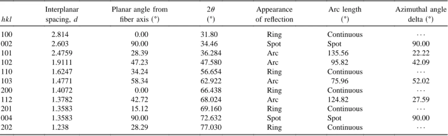
Debye – Scherrer XRD of the coatings confirmed that the ZnO was deposited with the piezoelectric wurtzite structure and that the columnar grains had a k001l orientation (the direction of polarization has not been determined) along the radius of the fiber (Fig. 15). For a perfectly radially oriented ZnO film, the diffraction pattern would have the appearance described in Table II. Of particular importance is the fact that the 002 and 004 reflections, as well as all higher order even 00l type reflections, would appear as spots for grains that are aligned with thek001l direction perpendicular to the fiber
FIG. 13. SEM image showing the ZnO fiber coating microstructure, which consists ofk001l radially oriented columnar grains.
FIG. 14. SEM image showing the approximately 0.5 mm grain size observed at the surface of a ZnO fiber coating.
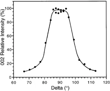
axis; i.e., the (002) and (004) planes are parallel to the fiber axis. Patterns obtained for sputter deposited ZnO fiber coatings exhibit arcs rather than spots for the 002 and 004 reflections, due to small radial misalignments for the columnar grains that compose the coatings. The collapse of the 002 ring into an arc is demonstrated by Fig. 16, which shows the intensity as a function of the azimuthal angular position along the 002 Debye ring. From the length of the arc, taken here as the full width at half maximum for the peak in Fig. 16, a deviation of 69.1±from perfect (002) alignment along the fiber axis is calculated.60
Due to the surface roughness of the ZnO coating, thin layers of Au (130 nm or less) did not result in contin-uous surface coatings that could be used for electrodes. In order to ensure that the top electrodes provided for good electrical contacts that were conducting over the surface of the ZnO, Au layers of at least 300 nm were required. As shown in Fig. 17, the Au coating looks like a snow cap on the columnar ZnO grains.
FIG. 15. Densitometer scan of a Debye – Scherrer XRD pattern for a CryAuyZnO coated optical fiber. The enhanced intensity of the 002 and 004 reflections indicatesk001l radial texture of the ZnO coating. PFOM devices with the structures described above have been tested for their piezoelectric response and phase modulation capabilities. Measurements with an all-fiber Mach-Zehnder interferometer have shown that phase shifts of up to 0.38 radyV can be achieved at the radial resonance frequency of 196.5 MHz.61 Although the largest phase shift response is obtained at the fiber radial resonances, the phase shifting capabilities have been demonstrated over the frequency range of 50 Hz to 800 MHz.62,63 Detailed optical and the electrical characterization of the PFOM devices will be described in future publications.
IV. CONCLUSIONS
Fabrication of PFOM devices has required studies in three general areas: fiber cleaning to ensure adhe-sion of evaporation CryAu electrode coatings on glass
fibers with different compositions, reactive magnetron sputtering of Zn to produce ZnO coatings at high rates, and microstructural characterization of fiber coatings to confirm the proper device structure.
It was determined that standard telecommunication fiber could be sufficiently cleaned by using a series of organic solvents to strip the protective polymer coating and wash the fiber surface. Evaporated CryAu coatings exhibited good adhesion on the chemically cleaned stan-dard fibers. High-strength fibers with an extra layer of Ti-doped glass over-cladding required a chemical wash as well as a thermal treatment at 300±C or higher temperatures to ensure adhesion of evaporated CryAu electrodes.
By investigating the dc magnetron sputtering of Zn as a function of PO2 and P, sputtering conditions for obtaining high deposition rates of ZnO have been determined for the fabrication of PFOM devices. Three regions of R vs PO2 behavior have been observed on approaching the oxide to metal sputtering mode transi-tion, Pc, from the high PO2side. For the oxide sputtering mode, a transition between oxygen and argon dominated sputtering is observed in all three R vs PO2 regions when the total pressure is varied and PO2 is held constant. The transition between oxygen and Ar dominated sputtering occurs at the fractional Ar pressure FAr 0.28 6 0.03 for all three R vs PO2 regions with an applied target power of 250 W. The highest deposition rates that can be obtained while still maintaining the oxide sputtering mode are observed when PO2 is within the R vs PO2 region II with FAr . 0.28.
PFOM devices were prepared by evaporating elec-trode layers and sputtering ZnO layers, while device structuring was accomplished by shadow masking tech-niques. SEM and Debye – Scherrer XRD confirmed the structural requirements for PFOM operation. Axially symmetric coatings of ZnO deposited onto CryAu coated fibers exhibited a columnar microstructure with k001l radially oriented grains. Coatings of ZnO and CryAu
TABLE II. Calculated appearance of Debye – Scherrer x-ray diffraction pattern for a ZnO fiber coating withk001l radial texture.
Interplanar Planar angle from 2u Appearance Arc length Azimuthal angle
hkl spacing, d fiber axiss±d s±d of reflection s±d deltas±d
100 2.814 0.00 31.80 Ring Continuous · · · 002 2.603 90.00 34.46 Spot Spot 90.00 101 2.4759 28.39 36.284 Arc 135.56 22.22 102 1.9111 47.23 47.580 Arc 95.82 42.09 110 1.6247 34.24 56.654 Ring Continuous · · · 103 1.4771 58.34 62.922 Arc 75.96 52.02 200 1.4072 0.00 66.438 Ring Continuous · · · 112 1.3782 42.72 68.024 Arc 124.82 27.59 201 1.3583 15.12 69.160 Ring Continuous · · · 004 1.3583 90.00 72.632 Spot Spot 90.00 202 1.238 28.29 77.030 Ring Continuous · · ·
FIG. 16. Relative intensity of the 002 ZnO XRD reflection vs azi-muthal angle delta. The intensity peak at d 90±confirms that the 002 planes are parallel with the fiber axis and the full width at half maximum indicates a deviation of 69.1±.
FIG. 17. SEM fracture cross-section image of the top electrode for a PFOM device.
with parabolic thickness distributions that varied less than 25% and 15%, respectively, were deposited on 8 cm sections of fiber. Top electrode coatings of greater than 0.3 mm were required because the rough sur-face of the 5 to 6 mm thick ZnO coating could not be continuously covered with thinner coatings. Optical phase shifting capabilities of the ZnO-based PFOM devices have been demonstrated for a frequency range of 50 Hz to 800 MHz, and a maximum phase shift of 0.38 radyV has been achieved at the 196.5 MHz fiber radial resonance.
ACKNOWLEDGMENTS
The authors would like to thank Thomas Maeder, Louis-Henri Masson, and Jos´e Llambias for their helpful
discussions on the design of the fiber coating equipment and Pedro Moeckli for help with the Debye-Scherrer x-ray diffraction analysis. We also would like to thank Roman Gubser at the Laboratorium f¨ur Kristallographic, Department f ¨ur Erdwissenschaften, ETH Zurich for use of the densitometer for the Debye-Scherrer film analy-sis. This work was supported by the Optical Sciences, Applications, and Technology, Priority Program of the Board of the Swiss Federal Institute of Technology.
REFERENCES
1. L. J. Donalds, W. G. French, W. C. Mitchell, R. M. Swinehard, and T. Wei, Electron Lett. 18, 327 (1982).
2. J. Jarzynski, J. Appl. Phys. 55 (9), 3243 (1984).
3. H. F. Taylor, IEEE J. Lightwave Technol. LT-5 (7), 990 (1987). 4. M. Imai, T. Yano, K. Motoi, and A. Odajima, IEEE J. Quantum
Electron. 28 (9), 1901 (1992).
5. M. D. Mermelstein, Appl. Opt. 22 (7), 1006 (1983).
6. M. Imai, H. Tanizawa, Y. Ohtsuka, Y. Takase, and A. Odajima, J. Appl. Phys. 60 (6), 1916 (1986).
7. M. L. Wilson, U.S. patent number 4,929,050 (1990). 8. A. Odajima and M. Imai, Ferroelectrics 92, 41 (1989). 9. M. Imai, T. Yano, Y. Ohtsuka, K. Motoi, and A. Odajima, IEEE
Photon. Technol. Lett. 2 (10), 727 (1990).
10. B. L. Heffner and B. T. Khuri-Yakub, Appl. Phys. Lett. 48 (21), 1422 (1986).
11. B. L. Heffner, W. P. Risk, B. T. Khuri-Yakub, and G. S. Kino, IEEE Ultrason. Symp. Proc., 709 (1986).
12. A. A. Godil, D. B. Patterson, B. L. Heffner, G. S. Kino, B. T. Khuri-Yakub, IEEE J. Lightwave Technol. 6 (10), 1586 (1988). 13. F. S. Hickernell, G. M. Reese, H. D. Knuth, T. P. Emmons, J. F.
Weller, and D. S. Czaplak, IEEE Ultrason. Symp. Proc. 715 (1986).
14. D. S. Czaplak, J. F. Weller, L. Goldberg, F. S. Hickernell, H. D. Knuth, and S. R. Young, IEEE Ultrason. Symp. Proc., 491 (1987). 15. F. S. Hickernell, IEEE Ultrason. Symp. Proc., 417 (1988). 16. B. T. Khuri-Yakub, G. S. Kino, and P. Galle, J. Appl. Phys. 46
(8), 3266 (1975).
17. S. Maniv and A. Zangvil, J. Appl. Phys. 49 (5), 2787 (1978). 18. I. Petrov and V. Orlinov, Thin Solid Films 120, 55 (1984). 19. S. B. Krupanidhi and M. Sayer, J. Appl. Phys. 56 (11), 3308
(1984).
20. N. Tsuji, H. Komiyama, and K. Tanaka, Jpn. J. Appl. Phys. 29 (5), 835 (1990).
21. S. Maniv, W. D. Westwood, and E. Colombini, J. Vac. Sci. Technol. 20 (2), 162 (1982).
22. J. Hrbek, Thin Solid Films 42, 185 (1977).
23. J. Roth, in Sputtering by Particle Bombardment II, edited by R. Behrisch (Springer-Verlag, New York, 1983), pp. 91 – 146. 24. W. D. Westwood, Physics of Thin Films, edited by M. H.
Fran-combe and J. L. Vossen (Academic Press, Inc., San Diego, CA, 1989), Vol. 14, pp. 1 – 73.
25. Fiber type FSN-10y125y250, and FS(Ti)-10y125y250, Cabloptic SA, Cortaillod, Switzerland.
26. Dichloromethane, 99.9% HPLC grade, Aldrich Chemie GmbH & Co. KG, Steinheim, Germany.
27. Acetone, 99.91% HPLC grade, Aldrich Chemie GmbH & Co. KG, Steinheim, Germany.
28. 2-propanol, 99.5% HPLC grade, Aldrich Chemie GmbH & Co. KG, Steinheim, Germany.
29. Scotch Magic, 810, adhesive tape, 3M, USA.
30. M. Ohring, The Materials Science of Thin Films (Academic Press, Inc., Boston, MA, 1992), p. 445.
31. Cement Universal, Merz and Benteli SA, Niederwangen, Switzer-land.
32. 306 Evaporator, Edwards High Vacuum International, West Sus-sex, U.K.
33. FTM5 digital film thickness monitor, Edwards High Vacuum International, West Sussex, U.K.
34. Chrome Plate Tungsten Rods, CRW1, R.D. Mathis Company, Longbeach, CA.
35. Au wire, 0.05 mm diameter, 99.99% pure, Metalor SA, Switzer-land.
36. Mo boat, ME9-.005MO, R.D. Mathis Company, Longbeach, CA. 37. Zn target, 99.99% pure, CERAC Incorporated, Milwaukee, WI. 38. Diffusion pump, diffstak 160y700C, Edwards High Vacuum
In-ternational, West Sussex, U.K.
39. Rotary vacuum pump, E2M28, Edwards High Vacuum Interna-tional, West Sussex, U.K.
40. VAT gate valve, series 64, and adaptive pressure controller PM-5, VAT aktiengesellschaft f¨ur Vakuum-Apparate-Technik, Haag, Switzerland.
41. Mass flow controller, type 825, and multi-channel flow controller, model 1605, Edwards High Vacuum International, West Sussex, U.K.
42. 120A Baratron, MKS Instruments, Inc., Andover, MA. 43. Magnetron sputtering source, 4 inch diameter, Edwards High
Vacuum International, West Sussex, U.K.
44. dc power supply, MD-1X, Advanced Energy Industries GmbH, Filderstadt, Germany.
45. STM 100yMF Thickness Monitor/Rate Monitor, Sycon Instru-ments, East Syracuse, NY.
46. Alpha-Step 200, Tencor Instruments, Mountain View, CA.
47. [100] oriented, n-doped, Si wafers, CSEM, Neuchˆatel, Switzer-land.
48. Debye – Scherrer camera, Huber, Rimsting, Germany.
49. Kodak diagnostic film, SB-392, Eastman Kodak Company, Rochester, NY.
50. Densitometer, Carl Zeiss, Germany.
51. Scanning Electron Microscope, S360, Cambridge Instruments, England.
52. Scanning Electron Microscope, JEOL 6300 F, JEOL Ltd., Japan. 53. EPOFIX Resin, Struers, Copenhagen, Denmark.
54. I. H. Khan, in Handbook of Thin Film Technology, edited by L. I. Maissel and R. Glang (McGraw-Hill, Inc., New York, 1970), pp. 10.1 – 10.65.
55. S. Kadlec, J. Musil, and J. Vyskocil, Vacuum 37 (10), 729 (1987). 56. T. Larsson, H-O. Blom, C. Nender, and S. Berg, J. Vac. Sci.
Technol. A 6 (3), 1832 (1988).
57. C. Plog, L. Wiedmann, and A. Benninghoven, Surf. Sci. 67, 565 (1979).
58. K. Wittmaack, Surf. Sci. 89, 668 (1979).
59. A Roth, Vacuum Technology (North-Holland Publishing Com-pany, New York, 1982), pp. 33 – 44.
60. B. D. Cullity, Elements of X-Ray Diffraction, 2nd ed. (Addison-Wesley Publishing Company, Inc., Reading, MA, 1978), pp. 300 – 303.
61. G. R. Fox, C. A. P. Muller, N. Setter, N. H. Ky, and H. G. Limberger, J. Vac. Sci. Technol. A 14 (3) (1996).
62. N. H. Ky, H. G. Limberger, R. P. Salath´e, and G. R. Fox, IEEE J. Lightwave Technol. 14 (1), 23 (1996).
63. N. H. Ky, H. G. Limberger, R. P. Salath´e, and G. R. Fox, IEEE Photon. Technol. Lett. 8 (5), 629 (1996).