Publisher’s version / Version de l'éditeur:
Applied Optics, 47, 13, pp. C231-C245, 2008-05-01
READ THESE TERMS AND CONDITIONS CAREFULLY BEFORE USING THIS WEBSITE. https://nrc-publications.canada.ca/eng/copyright
Vous avez des questions? Nous pouvons vous aider. Pour communiquer directement avec un auteur, consultez la
première page de la revue dans laquelle son article a été publié afin de trouver ses coordonnées. Si vous n’arrivez pas à les repérer, communiquez avec nous à [email protected].
Questions? Contact the NRC Publications Archive team at
[email protected]. If you wish to email the authors directly, please see the first page of the publication for their contact information.
NRC Publications Archive
Archives des publications du CNRC
This publication could be one of several versions: author’s original, accepted manuscript or the publisher’s version. / La version de cette publication peut être l’une des suivantes : la version prépublication de l’auteur, la version acceptée du manuscrit ou la version de l’éditeur.
Access and use of this website and the material on it are subject to the Terms and Conditions set forth at
2007 Topical Meeting on Optical Interference Coatings: Manufacturing
Problem
Dobrowolski, J. A.; Browning, Stephen; Jacobson, Michael; Nadal, Maria
https://publications-cnrc.canada.ca/fra/droits
L’accès à ce site Web et l’utilisation de son contenu sont assujettis aux conditions présentées dans le site LISEZ CES CONDITIONS ATTENTIVEMENT AVANT D’UTILISER CE SITE WEB.
NRC Publications Record / Notice d'Archives des publications de CNRC:
https://nrc-publications.canada.ca/eng/view/object/?id=8b856e90-9a7d-47e0-864c-1c72b34e4b6e https://publications-cnrc.canada.ca/fra/voir/objet/?id=8b856e90-9a7d-47e0-864c-1c72b34e4b6e2007 Topical Meeting on Optical Interference Coatings:
Manufacturing Problem
J. A. Dobrowolski,1,* Stephen Browning,2Michael Jacobson,3 and Maria Nadal4
1National Research Council, 1500 Montreal Road, Ottawa, Ontario, Canada, KIA 0R6
2Ball Aerospace & Technologies Corporation, 1600 Commerce Street, Boulder, Colorado 80301, USA 3Optical Data Associates, 5237 E. Seventh Street, Tucson, Arizona 85711
4National Institute of Standards and Technology, 100 Bureau Drive, Stop 8442, Gaithersburg, Maryland 20899, USA
*Corresponding author: [email protected]
Received 29 August 2007; accepted 10 May 2007;
posted 12 December 2007 (Doc. ID 86942); published 31 January 2008
Measurements are described on the experimental filters submitted to the Third Optical Thin Film Manufacturing Problem in which the object was to produce multilayers with a measured colorimetric performance that is as close as possible to that specified. The perceived colors of the coating, when illuminated with randomly polarized light incident at 7° by a source representing average daylight with a correlated color temperature of approximately 6500 K, were to be yellow and blue, respectively, in light reflected from its two surfaces, and the color was to appear white when viewed in transmission mode. Eleven teams from 7 different countries submitted a total of 18 samples. © 2008 Optical Society of America
OCIS codes: 120.2440, 310.1620, 310.1860.
1. Introduction
The aim of Manufacturing Problems at the Optical Society of America Topical Meetings on Optical In-terference Coatings (OIC) is to test the current state of the art of the manufacture of various kinds of multilayers having a specified performance [1,2]. The participants select a multilayer design with which they feel they can produce the closest match to the specifications. Thus the number of layers, coating materials, and overall thickness of the multilayers and the process used to implement it is entirely under their control. Only two restrictions are imposed. For safety considerations, the use of toxic materials is discouraged. For ease of measurement, the coatings must be deposited on standardized substrates. The measurements of the samples are performed in two different laboratories. To encourage participation, only transmission and reflection measurements are performed on the samples, which are returned to their owners after the event. There is no need to disclose the actual materials and deposition
pro-cesses used, although the participants are encour-aged to provide whatever information they can share without compromising the interests of their organi-zations. The participants have to provide their measurement of the normal incidence spectral trans-mittance of their sample as well as the thicknesses and optical constants at the central wavelength of the layers of their system so that the refractive index profile of their multilayer can be plotted. Both these pieces of information are invaluable to the organizers for the resolution of problems during the measure-ment and evaluation of the samples.
This paper describes the 2007 Manufacturing Problem and the performance of the submitted sam-ples. The basic premise of the exercise has not been changed. However, one significant change in the pro-cedure was introduced this time. The submitted sam-ples were not linked to the names of the participants in either the oral presentation or in this written re-port. On arrival, each sample was assigned a random three-letter code that was known only to the two main organizers of the event and to the producer of the sample. The participants were thus able to rec-ognize and see the ranking of their contribution within the list of all samples, but they did not know
0003-6935/08/130C231-15$15.00/0 © 2008 Optical Society of America
the names of the producers of the other samples. This change does not in any way detract from the main goal of the exercise—the examination of the present state of the art of optical thin-film manufacture. How-ever, it was deemed that this degree of anonymity might permit more people to participate in the exer-cise, an assumption that was borne out in practice. Another change was that, to simplify the measure-ments and reduce the possibility of the introduction of errors during the evaluation of the coatings, the multilayer coatings were deposited on standard plane parallel fused-quartz substrates provided by the or-ganizers.
2. Definition of the Problem
The solution to this third Manufacturing Problem was defined entirely in Commission Internationale de l’Eclairage (CIE) standard colorimetric terms [3,4]. The requirement was that the perceived color of the coating, when illuminated at near-normal incidence by a source representing average daylight with a correlated color temperature of approxi-mately 6500 K (CIE Standard Illuminant D65), would be yellow and blue, respectively, in light re-flected from its two surfaces A and B, and it would appear to be white when viewed in transmission. The three beams m ⫽ 1, 2, and 3 were to appear to be of equal luminous reflectance or transmittance YT.
Specifically, the target performance was defined as shown in Table 1.
The merit function (MF) used to judge the perfor-mance of the submitted samples was
MF ⫽
再
1 9冋
m⫽1兺
3冉
xm T⫺ x m 0.01xmT冊
2 ⫹兺
m⫽1 3冉
ym T⫺ y m 0.01ymT冊
2 ⫹兺
m⫽1 3冉
YmT⫺ Ym 0.01YmT冊
2册冎
1兾2 . (1)In the above, xmT, ymT, YmTand xm, ym, Ymare the target
and experimentally measured CIE x and y chroma-ticity coordinates and CIE tristimulus value Y, re-spectively. These quantities depend directly on the spectral reflectances and the transmittance of the sample. They are given by the expressions
xm⫽ Xm兾共Xm⫹ Ym⫹ Zm兲 ym⫽ Ym兾共Xm⫹ Ym⫹ Zm兲, (2) where m ⫽ 1, 2, 3. Here Xm⫽ k
冕
L U x共兲S共兲qm共兲d, Ym⫽ k冕
L U y共兲S共兲qm共兲d, Zm⫽ k冕
L U z共兲S共兲qm共兲d, (3)where x共兲, y共兲, z共兲 are the CIE 1931 (2°) Standard Observer color-matching functions defined within the wavelength range L⫽380 nm to U⫽780 nm at 5
nm intervals. In Eq. (3), S共兲 is the spectral power distribution of the specified CIE standard illuminant D65, and qm共兲 for m ⫽ 1, 2, or 3 corresponds to the
spectral reflectances RA共兲, RB共兲 of the surfaces A
and B and the spectral transmittance T共兲 of the sample, all measured in unpolarized light incident at 7°. In the case of reflecting or transmitting samples, the Y tristimulus value also represents the luminous reflectance or transmittance, where the constant k in Eq. (3) is defined by the following expression:
k ⫽ 100
冒
冕
L U
y共兲S共兲d, (4) giving a Y value of 100 for the perfect reflecting or transmitting sample.
It is perhaps appropriate at this time to remind the reader that it has been known for a long time that in the presence of absorbing layers the reflectances can be quite different for light incident onto the multi-layer from opposite directions (see, for example, [5]). This effect has been exploited in some types of de-signer sunglasses where the transmitted beam must be neutral and where the color of the first surface is chosen for decorative purposes, but where the color of the second surface reflected beam is of no conse-quence (see [6]).
The two main types of instrument available for surface color measurement are colorimeters and spectrophotometers. Colorimeters give a direct mea-sure of the colorimetric quantities, but they do not provide any information on the underlying spectral reflectance or transmittance properties of the test samples. The results are only applicable to the spe-cific measurement geometry of the instrument design and the illumination and observer conditions. Spec-trophotometers, on the other hand, provide detailed information of the spectral properties of the sample, can be configured for different measurement geome-tries, and result in more reliable determinations. It is for this reason that it was decided to use Eq. (1) with colorimetric data (CIE color coordinates and lumi-nance values) derived from measured
spectrophoto-Table 1. Definition of the Target Performance
m
CIE Standard Observer Color
Coordinate Targets xmT ymT YmT
1 Unpolarized light reflected from surface A at 7°
0.50 0.45 30 2 Unpolarized light reflected from
surface B at 7°
0.16 0.25 30 3 Unpolarized transmitted light at 7° 0.31 0.31 30
metric curves, rather than to use colorimeters for this purpose. The effect of the second surface of the sub-strate, which could or could not be coated, had to be included in the final measured performance of the sample.
The measurements were performed at two inde-pendent laboratories, the National Institute of Stan-dards and Technology (NIST) and Optical Data Associates (ODA), neither of which is allowed to sub-mit a solution to the Manufacturing Problem. It should be emphasized once again that significant dif-ferences in the final color values could result from the use of different wavelength increments, bandpasses, methods of interpolation of the measured data, etc. An Excel evaluation program was developed that con-verted the two reflectance and one transmittance curves (either calculated or measured on a spectro-photometer) into CIE color coordinates and lumi-nances and which then evaluated from this data the value of the merit function of the system. This pro-gram was used in the preliminary investigation of the problem (Section 3), as well as in the evaluation of the measurements from the two measurement laborato-ries of the submitted samples. The same program, together with a sample data set, was also sent to the participants to assist them in the in-house design and evaluation of their own solutions.
3. Discussion of the Problem
A number of commercial thin-film programs are available that permit the design of filters defined in terms of color coordinates. Because in the present example the target reflectances from the two sides of the substrate are different, the solutions had to con-tain at least one absorbing layer. This was thus the first Manufacturing Problem that required the use of absorbing coating materials. Since the target values of the luminous transmittance and reflectances were specified to be the same, the amount of absorption introduced into the system had to be carefully con-trolled. The optical constants of absorbing coating materials are, on the whole, more difficult to repro-duce than the refractive indices of dielectric films. Because dielectric coatings are deposited onto the metal layers, and frequently oxygen is present during this process, it is necessary either to protect the metal from oxidation or to deposit thicker than necessary thicknesses of the metals to compensate for the re-duction in metal layer thickness (see, for example, [7]). Furthermore, the optical constants of metals de-pend often on the thicknesses of the layers [8] and they may change over time. For all these reasons, the deposition of precise and stable thin metallic films was deemed to be the main challenge in this Manu-facturing Problem.
Before such a problem could be proposed to the public, it was first necessary to establish that solu-tions to the problem do exist, that they could be based on any one of a number of different common and inexpensive metals, and that there are solutions that stand a fair chance of being manufactured. A study, in which 50 different layer systems were
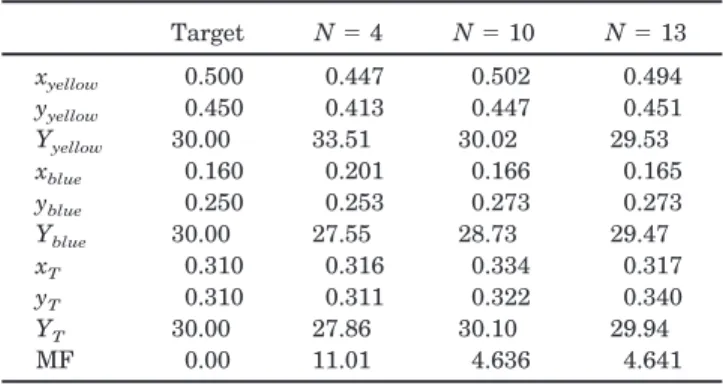
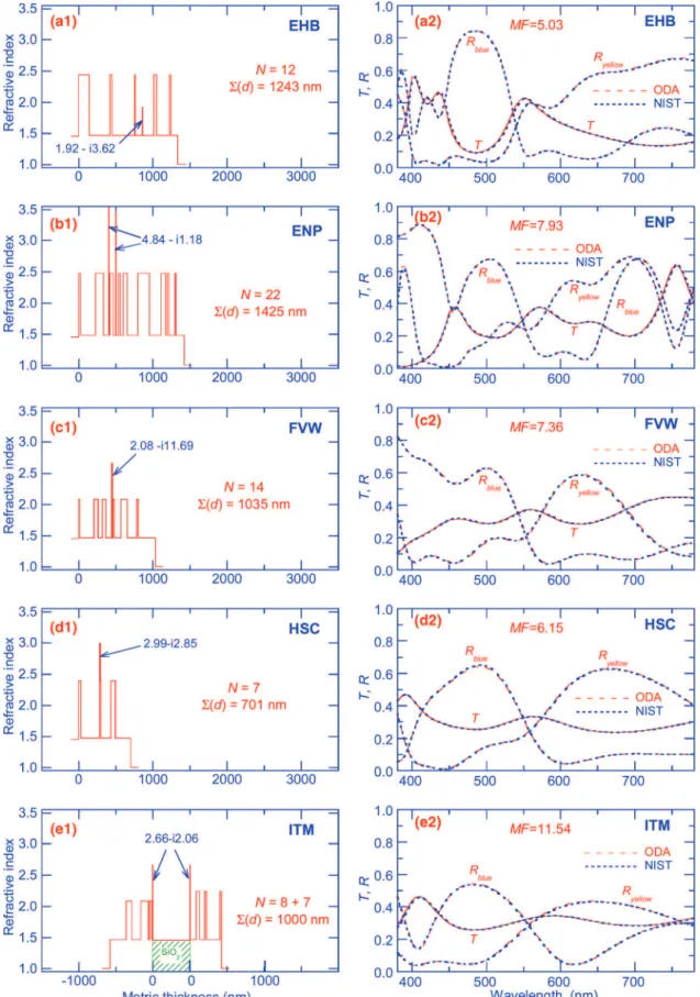
investi-gated, showed that solutions to the problem can be found and that they can be based on many different metals. These solutions can consist of different num-bers of layers and have different overall thicknesses. In Fig. 1, rows a, b, and c show the calculated results for three different solutions to the problem based on the use of three different thin metal layers in which it has been assumed that the substrate me-dium is of infinite extent. In column 1 are shown the refractive index profiles of the thin-film systems, the number of layers N, the overall metric thickness ⌺(d) of the system, and the optical constants (n ⫺ ik) of the metal layer. In column 2 are shown the calculated spectral transmittance T and reflectances Rblue,
Ryellowfor light incident onto the substrate from
op-posite sides at angles of incidence of 0° and 7°. It is obvious from this diagram that an angle of incidence of 7° results in a measurable, but not very significant, shift of the spectral curves toward shorter wave-lengths. Also shown is the value of the merit function MF of the system.
The solution depicted in Fig. 1(a) consists of only four layers of which one is made of Ni, and it has a total metric thickness of only 522 nm. Even though the calculated MF value of the system is high (MF ⫽ 11.01), the system’s colorimeric parameters (Table 2, column 3) indicate that the performance is not too far from that of the specified target values. The solution shown in Fig. 1(b) has 10 layers, of which one is made of Cr, and it has a total metric thickness of 737 nm. The calculated merit function of this system is 4.64, which is 2.5 times smaller than that of the system of Fig. 1(a). This is borne out by the colorimetric param-eters shown in Table 2, column 4. Finally, the system of Fig. 1(c) consists of 13 layers of 1203 nm total metric thickness and contains two Inconel layers. Its merit function value is also 4.64. A quick glance at the calculated spectral curves in Figs. 1(b) and 1(c) and at the colorimetric parameters in columns 4 and 5 of Table 2 shows that despite similar merit func-tions, the last two solutions are quite different. Similar solutions based on other metallic and semi-conductor layers have also been obtained. However, good reflectors, such as Ag, are not good candidate materials for this particular application.
In Figs. 2(a)–2(c) are shown the sensitivity of the calculated performances of the systems of Figs. 1(a)– 1(c) to random thickness variations of the individual layers of the systems. In addition to the solid curves, representing the theoretical calculated transmit-tance and reflectransmit-tance curves, the upper and lower boundaries within which one would expect 66% of experimentally measured curves to lie are also shown. These boundaries were obtained from calcu-lations on 50 systems with randomly perturbed thick-nesses of the layers. For the curves in column 1 the mean random thickness perturbations were 1%, a value of interest for the thicker layers of the system. In column 2 the mean perturbations were 1 nm, a value that is significant for the thinnest (mostly me-tallic) layers of the multilayer. For a system to be easily produced, the effects of both the 1% and 1 nm
random thickness perturbations should be small. From a cursory examination of Fig. 2 it is obvious that the effect of the 1 nm perturbations is more serious. This is not surprising—for example, a 1 nm change in the thickness of a 3 nm thick metal layer will have a significant effect on the amount of light absorbed by this layer. It is also worth noting that, although the 10- and 15-layer systems of Figs. 1(b)
and 1(c) have the same merit function values, their sensitivity to random errors is different. It has also been observed in the previous Manufacturing Prob-lems that the performance of solutions that consist of more than just the minimum numbers of layers re-quired for a satisfactory merit function appear to be more robust to random layer thickness perturbations. It is as if the additional layers provide an increased stability with respect to thickness errors.
It should be remembered that when the human eye is the detector, the significance of a given perturba-tion of a transmittance or a reflectance curve due to thickness errors will depend on the wavelength at which it occurs: It will be less important at either end of the spectrum than at the wavelength correspond-ing to the peak of the visibility curve. Nevertheless, the broad conclusions made above should still be valid.
The sensitivity of the performance of the solutions to random errors of the optical constants of the coat-ing materials has not been investigated. However, the degree within which the refractive indices of di-electric materials can be reproduced from run to run
Fig. 1. (Color online) Three different numerical solutions to the problem consisting of 4, 10, and 13 layers that are based on the use of Ni, Cr, and Inconel metal layers (rows a, b, c). In column 1 are shown the refractive index profiles of the solutions and in column 2 the calculated spectral transmittance and reflectance curves for unpolarized light incident at 0° and 7° incidence. In this figure, and in Figs. 3, 4, and 6, the reference wavelength for the optical constants is 550 nm.
Table 2. Target and Calculated Colorimetric Performance of Three Different Numerical Solutions
Target N ⫽ 4 N ⫽ 10 N ⫽ 13 xyellow 0.500 0.447 0.502 0.494 yyellow 0.450 0.413 0.447 0.451 Yyellow 30.00 33.51 30.02 29.53 xblue 0.160 0.201 0.166 0.165 yblue 0.250 0.253 0.273 0.273 Yblue 30.00 27.55 28.73 29.47 xT 0.310 0.316 0.334 0.317 yT 0.310 0.311 0.322 0.340 YT 30.00 27.86 30.10 29.94 MF 0.00 11.01 4.636 4.641
by most deposition methods is sufficient not to cause any problems. The challenge will be to accurately reproduce the extinction coefficients of the metals from one run to another or, alternatively, to devise a method for monitoring the metal layer absorption, rather than its thickness. All the above indicates that the manufacture of the coatings is possible, but not trivial, if good results are to be obtained.
It is necessary also at this point to discuss the effect of the second surface of the substrate. If left uncoated, it will reflect approximately 3.8% of the incident light across the visible spectrum. If layers are deposited on one surface of the substrate only, the performance of a series of solutions with an increasing number of layers based on a particular set of coating materials will eventually reach an asymptotic value. In Fig. 3(a) is shown a refractive index profile in which a substrate B of finite thickness with layer systems A, C applied to its two surfaces is shown. System A is the 15-layer system of Fig. 1(c), and system C is a two-material, 9-layer antireflection coating designed for an air– quartz interface. Figure 3(b) shows once again the spectral transmittance and reflectance curves of the 15-layer system [Fig. 1(c)] deposited onto a semi-infinite substrate. The performance of the same
coat-ing, deposited onto a substrate of finite thickness is shown in Fig. 3(c). It will be seen that the merit function has increased from 4.64 to a value of 6.50. If the nine-layer antireflection coating C is added to the second surface of the substrate B [Fig. 3(d)], the merit function of the combination will be 4.68. Of course, in practice the antireflection coating C could consist of fewer layers if more than two materials are used.
4. Participants
The Manufacturing Problem, as defined in Section 2, was circulated by mail to previous attendees of OIC and was posted on the OIC web site. Eleven different teams from 7 different countries submitted a total of 18 samples to the organizers of the Manufacturing Problem. In Table 3 the participants are listed in alphabetical order of the principal investigator’s name.
Four groups submitted two samples, and one group sent four samples. Three pairs of these samples were nominally the same, so the number of significantly different solutions submitted was 15. After having been assigned random names, the samples were sent to the measurement laboratories.
Fig. 2. (Color online) Sensitivity of the calculated performance of the systems of Figs. 1(a)–1(c) to random thickness variations: column 1—1% errors; column 2—1 nm errors (see text).
Most participants were generous in providing in-formation about the design, materials, and processes that they used in the manufacture of their samples.
Some of the comments provided are now listed. How-ever, to maintain anonymity, not listed is information (number of layers, overall thicknesses, materials)
Fig. 3. (Color online) Effect of the second surface reflection of the substrate on the performance of a single surface solution to the Manufacturing Problem. (a) Refractive index profiles of a 13-layer solution (A), the finite substrate (B), and a 9-layer antireflection coating (C). (b)–(d) Performance of the solution (A) on a semi-infinite substrate and on a finite thickness substrate (B) without and with the antireflection coating.
Table 3. Participants Listed in Alphabetical Order of the Principal Investigator’s Name
Number Name, Institution Postal Address E-mail Address Samples 1 S. Günster, I. Pauli, A. Tewes,
and D. Ristau, Laser Zentrum Hannover e.V.
Hollerithallee 8, 30419 Hannover, Germany
2 M. Lappschies, Laser Zentrum Hannover e.V.
Hollerithallee 8, 30419 Hannover, Germany
[email protected] 1 3 C-C. Lee, M-C. Liu, J-T. Lian,
and S-H. Chen, Dept. of Optics and Photonics, National Central University, Taiwan
Thin Film Technology Center, National Central University, 320 Taiwan
4 F. Lemarchand, Institut Fresnel Marseille, France [email protected] 1 5 P. Ma, National Research
Council
1200 Montreal Rd., Ottawa, Ontario K1A 0R6, Canada
[email protected] 2 6 I. MacMillan, Edmund Optics 601 Montgomery Ave.,
Pennsburg, PA 18073, USA
[email protected] 2 7 D. Poitras and A. Kuo, National
Research Council
1200 Montreal Rd., Ottawa, Ontario K1A 0R6, Canada
[email protected] 1 8 O. Prosovsky, FSUE
Technologiya
15 Kiev St., Obninsk 249035, Kaluga Reg., Russia
[email protected] 2 9 M. Tilsch et al., JDSU 2789 Northpoint Pkwy., Santa
Rosa, CA 95407, USA
[email protected] 2 10 A. Zangerl and G. Fuchs
Swarovski Optik KG
Swarovskistraße 70, A-6067 Absam, Austria
[email protected] 1 11 V. Zhupanov and E. Kluev,
Scientific Research Institute “Luch”
24 Zheleznodorozhnaya Podolsk, Moscow Reg. 142100, Russia
that would make possible the pairing of the samples to the participants.
Stefan Günster: The layer system was designed
with software developed at the Laser Zentrum Han-nover (LZH). The systems used for the deposition of the metal and dielectric layers were a Balzers BAK640 coater and a Syrus Pro plant with an APS IAD source, respectively. The LZH broadband spec-tral monitor was employed for the process control. No reoptimization or redesign was performed during the deposition process.
Marc Lappschies: The layers were deposited by
ion-beam sputtering from one metallic and one dielec-tric target. To produce the dielecdielec-tric layers, the sput-tering process took place in the presence of oxygen. The metallic target without oxygen in the deposition chamber was used to produce the absorbing layer. Broadband optical monitoring in the visible spectral region was used to control the individual layer thick-nesses. The time required to deposit the complete system was 5.5 h.
Cheng-Chung Lee in 1985 prepared metal–
dielectric coatings for a company making sunglasses and this is what motivated him to ask his students to participate in the Manufacturing Problem. They used a simple electron-beam gun coater without an ion source or plasma; the substrate was not heated. The metal layer and the high-index dielectric layers were based on the same element. The difference between the calculated and the measured merit function val-ues is believed to be due to the discrepancy between the assumed and actual optical constants of the metal layer. If they were to repeat the experiment, they would either use a very high vacuum for the metal layer evaporation or use sputtering to deposit it.
Fabien Lemarchand: The deposition technology
used was reactive low-voltage ion plating as imple-mented in a Balzers BAK 800 system. The chamber was equipped with a broadband optical monitoring system that simultaneously measured both transmit-tance and reflectransmit-tance at normal incidence in the 400 – 1000 nm spectral range. The monitoring system is described in detail in a paper by Badoil et al. [9]. The design of the multilayer system was found with the same global optimization method that was used by our team in the 2007 OIC Design Problem [10]. All our work has been performed using the definition of the problem as first posted in September. The calcu-lated merit function of the system that we decided to implement was MF ⫽ 2.56. This design was not the best in terms of merit function (we found a design with a value MF ⫽ 1.90), but it seemed to be the best compromise between theoretical performance and manufacturability. It required only one side of the fused-silica substrate to be coated. The deposition of the first dielectric layers onto the fused-silica sub-strate at 180 °C did not present any problems at all— the theoretical and measured reflectance and transmittance curves were in perfect agreement. However, there were many difficulties during the deposition of the absorbing layer. The optical con-stants depended on the thickness of the layer and on
the substrate temperature. Its spectral behavior changed first on the introduction of oxygen into the chamber due to partial oxidation that resulted in a reduction of its thickness by 1.5 nm and then again when an argon plasma was established, at which time the metal thickness was further reduced by 2 nm. Clearly our initial assumption that the absorbing layer is homogeneous was not fulfilled. The deposi-tion of the final dielectric layer of the system was terminated when a partial merit function consisting of the six colorimetric terms pertaining to the reflec-tance and transmitreflec-tance of the sample were mini-mized. When the sample was measured ex situ in a PerkinElmer Lambda 18 spectrophotometer with a V-W accessory at an angle of incidence of 7.5°, a merit function value of 2.77 was obtained.
Penghui Ma: The design was produced with
soft-ware developed at the NRC. The samples were made on our fully automated dual magnetron sputtering system equipped with an in situ wideband optical monitor [11]. For this Manufacturing Problem, oxide layers were reactively sputtered from two metallic targets, one of which was a mixture of two elements. The thickness of the metal layer was reduced by ox-idation during the deposition of the next oxide layer. The thickness reduction was determined in a prelim-inary experiment using in situ transmittance mea-surements and allowed for in the final design.
Iain MacMillan: The designs were produced
us-ing TFCALC software. The dielectric and metal lay-ers were deposited in separate chamblay-ers from materials supplied by Edmund Optical. The metal layers were deposited by e-gun evaporation in a 25 in. chamber at ambient temperature (1 in. ⫽ 2.54 cm). The dielectric layers were deposited using e-gun evaporation with ion assist in a 45 in. chamber at 150 °C. The total time for the development and sam-ple production was of the order of 3– 4 days.
Daniel Poitras: The design was obtained with a
trial version of the OptiLayer program and TFArchi-tect, a proprietary software developed at the NRC [12]. The metal and dielectric layers were deposited in a dual ion-beam sputtering system (SPECTOR by Veeco-IonTech) equipped with a NRC-developed wideband optical monitor. The system was fully au-tomated and incorporated thickness determination and design reoptimization. In the design, the thin metal layer was surrounded by oxide materials. To prevent the oxidation of this thin metal layer during the deposition of the following oxide layer, we depos-ited an approximately 1.5 nm thick amorphous sili-con layer on it [7]. This was fully oxidized during the deposition of the following oxide layer but protected the metal from oxidation. No attempts were made to measure the performance of the coating other than to check the final monitoring transmission curve ob-tained when the fabrication was finished.
Markus Tilsch: Ours was truly a team effort: The
et al. in the table stands for Adam Bergeron, Marius
Grigonis, Karen Hendrix, Georg Ockenfuss, Robert Sargent, Joe Smith, Kaz Takano, and Tom Yanes, who all contributed significantly. The parts were
Fig. 4. (Color online) Measurement results. The results for the significantly different solutions submitted by the participants are shown in rows a– o. In column 1 are shown the refractive index profiles of the solutions and in column 2, the measured spectral transmittance and reflectance curves for unpolarized light incident at 7° incidence obtained at NIST and ODA.
coated in our new platform Ucp-1 that is based on magnetron sputtering. The machine is equipped with a load lock. So far our Ucp-1 focus had not been on
absorbing materials. For the Manufacturing Prob-lem, we performed a few tests with our materials at hand. We selected a process for making the absorbing
material and demonstrated good repeatability. The deposition of the dielectric and the absorptive layers was fully automatic and it was done in one run. Three
iterations were needed to produce the samples for the contest during which the information on the absorb-ing material was progressively refined and the design
suitably adjusted. Once we received substrates from the organizers, we had to be creative on the way to hold and coat them. The coating time from the start to the end of run was 18 min for our first sample and 18 and 13 min for the two sides of our second sample. Six 200 mm diameter wafers could be produced uni-formly in that coating time. For more information, see the link to a JDSU publication on the Ucp-1 sys-tem: JDSU Ucp-1 paper [13].
Alois Zangerl: The equipment that we used for
the deposition of our sample was a Balzers BAK760 with new process control software and a 2 Ferrotec-e-beam-evaporator with a Mark II ion source, pumped by a cryo-pump with an in situ broadband optical monitor operating on rotating substrates.
Valery Zhupanov: OptiLayer software was used
to obtain the metal– dielectric design. The system was deposited in a cryogenically pumped Leybold A-1100 vacuum coater. An e-gun was used to deposit the two oxide and the metal layers. The rates of dep-osition for the high- and low-index oxide layers were 0.2 and 0.5 nm兾s, respectively. An end-Hall-type ion source was employed for IAD with oxygen. No ion assist was used during the deposition of the metal film. After the metal layer was deposited, during the first stages of deposition of the adjoining oxide layer, the ion beam remained turned off to prevent oxida-tion of the metal layer. The ion beam was switched on again only after the metric thickness of the oxide layer exceeded 4 –5 nm. In situ measurements of the optical thicknesses of the coatings were carried out on a test glass located at the center of the chamber using a broadband spectrometer operating in the 380 –1100 nm spectral region. The deposition of each layer was terminated when the best fit was obtained between the measured and the calculated transmission curves of the partial system. The transmission and reflection spectrum of the finished system was then measured
ex situ with a Cary-300 spectrophotometer. The data
obtained from these measurements was then entered into the OptiRe software to find the errors in the layer
thicknesses. The evaporation process was repeated with thickness corrections based on these calcula-tions.
5. Measurement Equipment
As in the previous two Manufacturing Problems, the measurements were performed at NIST and at ODA. At NIST the instrument used for the measurements was a commercial Lambda 950 PerkinElmer spectro-photometer with a Universal Reflectance Accessory. Measurements were performed in the wavelength range from 380 to 780 nm at 5 nm increments with a 5 nm bandpass and a wavelength resolution of 0.08 nm. The sources used were tungsten halogen and deu-terium lamps and the detector was a photomultiplier. The geometry for the reflectance measurements was 8° specular angle, and for the transmittance measure-ments the samples were slightly tilted to approxi-mately 7°.
At ODA the measurements were performed on a Cary 5000 UV–Vis–NIR double-grating, double-beam spectrophotometer that is capable of operating in the 180 ⬍ ⬍ 3300 nm spectral range. The horizontal and vertical f numbers and the maximum departures of the illuminating beam from the principal direction were 9, 7.2 and 0.8°, 1.9°, respectively. The sources employed were also tungsten– halogen and deute-rium lamps. The detector used was an UV-extended photomultiplier. A conservative error estimate for oblique angle measurements in the 400 ⬍ ⬍ 600 nm spectral range was 0.4%.
At this point it is worth mentioning that a compar-ison of the measurements with the normal incidence transmission curves and with calculations based on the refractive index profiles provided by the partici-pants was of great assistance in determining which measurements should be repeated, or indeed, if the provided refractive index profiles were correct. It will be seen from Fig. 4 that the agreement between the measurements performed at the two laboratories was excellent.
Table 4. Target and Measured Average Colorimetric Performance of the 15 Significantly Different Samples
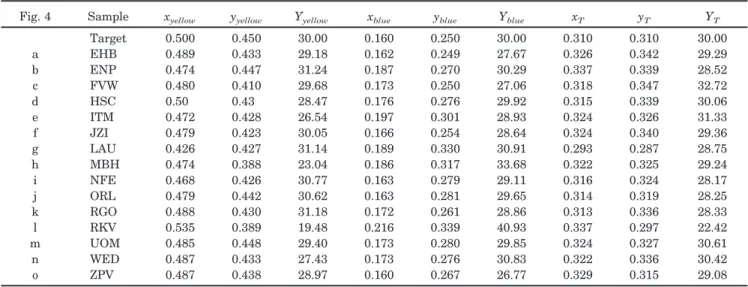
Fig. 4 Sample xyellow yyellow Yyellow xblue yblue Yblue xT yT YT
Target 0.500 0.450 30.00 0.160 0.250 30.00 0.310 0.310 30.00 a EHB 0.489 0.433 29.18 0.162 0.249 27.67 0.326 0.342 29.29 b ENP 0.474 0.447 31.24 0.187 0.270 30.29 0.337 0.339 28.52 c FVW 0.480 0.410 29.68 0.173 0.250 27.06 0.318 0.347 32.72 d HSC 0.50 0.43 28.47 0.176 0.276 29.92 0.315 0.339 30.06 e ITM 0.472 0.428 26.54 0.197 0.301 28.93 0.324 0.326 31.33 f JZI 0.479 0.423 30.05 0.166 0.254 28.64 0.324 0.340 29.36 g LAU 0.426 0.427 31.14 0.189 0.330 30.91 0.293 0.287 28.75 h MBH 0.474 0.388 23.04 0.186 0.317 33.68 0.322 0.325 29.24 i NFE 0.468 0.426 30.77 0.163 0.279 29.11 0.316 0.324 28.17 j ORL 0.479 0.442 30.62 0.163 0.281 29.65 0.314 0.319 28.25 k RGO 0.488 0.430 31.18 0.172 0.261 28.86 0.313 0.336 28.33 l RKV 0.535 0.389 19.48 0.216 0.339 40.93 0.337 0.297 22.42 m UOM 0.485 0.448 29.40 0.173 0.280 29.85 0.324 0.327 30.61 n WED 0.487 0.433 27.43 0.173 0.276 30.83 0.322 0.336 30.42 o ZPV 0.487 0.438 28.97 0.160 0.267 26.77 0.329 0.315 29.08
6. Measurement Results
In this section the results for the significantly dif-ferent solutions submitted by the participants are presented. All the samples submitted by the partic-ipants were measured, but, in the case of the three pairs of nominally identical pairs, results are given only for the sample with the best performance in each pair.
The results for the different solutions are shown in rows a– o of Fig. 4. They are presented in alphabetical order of their randomly assigned codes. In column 1 are shown the refractive index profiles of the
solu-tions. For easier comparison, the same metric thick-ness scale is used throughout this figure. In each diagram, arrows indicate the location of the absorb-ing layers, and the optical constants provided by the participants for these layers are given. Also listed are the number of layers and the total metric thickness of the system. In column 2, the spectral transmittance and reflectance curves measured at NIST and ODA for unpolarized light incident at 7° are given. Also listed is the average of the merit functions calculated according to Eq. (1) from the measurements at these institutions.
Table 4 lists the target and average measured col-orimetric performance of the significantly different samples submitted to the Manufacturing Problem. To graphically depict the spread of the various solutions, the average measured x and y CIE chromaticity co-ordinates of the 15 samples are also shown in Fig. 5. Of course, it does not follow that the solution with the smallest average discrepancy between the target and measured values of the x and y CIE chromaticity coordinates is the best solution to the problem since this diagram does not contain any information on the luminous transmittance and reflectance values of the samples, which play an equally important role in this problem.
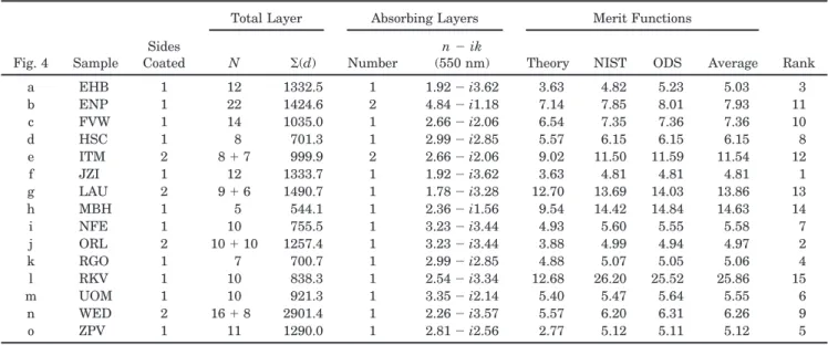
Table 5 provides information on the layer systems of the 15 significantly different samples, their cal-culated and measured merit function values, and their ranking. Listed are the number of surfaces coated, the number of layers in the solution, the number of absorbing layers, and their nominal op-tical constants at ⫽ 550 nm. Also shown are the following merit functions: the theoretical value pro-vided by the participants, the measured values at NIST and ODA, and the average measured value. This latter value establishes the ranking of the sample.
Fig. 5. (Color online) Measured x and y CIE chromaticity nates of all 18 samples. Also shown are the chromaticity coordi-nates of the specified targets.
Table 5. Information on the Layer Systems of the 15 Significantly Different Samples, Their Calculated and Measured Merit Function Values, and Their Ranking
Fig. 4 Sample
Sides Coated
Total Layer Absorbing Layers Merit Functions
Rank
N ⌺(d) Number
n ⫺ ik
(550 nm) Theory NIST ODS Average a EHB 1 12 1332.5 1 1.92 ⫺ i3.62 3.63 4.82 5.23 5.03 3 b ENP 1 22 1424.6 2 4.84 ⫺ i1.18 7.14 7.85 8.01 7.93 11 c FVW 1 14 1035.0 1 2.66 ⫺ i2.06 6.54 7.35 7.36 7.36 10 d HSC 1 8 701.3 1 2.99 ⫺ i2.85 5.57 6.15 6.15 6.15 8 e ITM 2 8 ⫹ 7 999.9 2 2.66 ⫺ i2.06 9.02 11.50 11.59 11.54 12 f JZI 1 12 1333.7 1 1.92 ⫺ i3.62 3.63 4.81 4.81 4.81 1 g LAU 2 9 ⫹ 6 1490.7 1 1.78 ⫺ i3.28 12.70 13.69 14.03 13.86 13 h MBH 1 5 544.1 1 2.36 ⫺ i1.56 9.54 14.42 14.84 14.63 14 i NFE 1 10 755.5 1 3.23 ⫺ i3.44 4.93 5.60 5.55 5.58 7 j ORL 2 10 ⫹ 10 1257.4 1 3.23 ⫺ i3.44 3.88 4.99 4.94 4.97 2 k RGO 1 7 700.7 1 2.99 ⫺ i2.85 4.88 5.07 5.05 5.06 4 l RKV 1 10 838.3 1 2.54 ⫺ i3.34 12.68 26.20 25.52 25.86 15 m UOM 1 10 921.3 1 3.35 ⫺ i2.14 5.40 5.47 5.64 5.55 6 n WED 2 16 ⫹ 8 2901.4 1 2.26 ⫺ i3.57 5.57 6.20 6.31 6.26 9 o ZPV 1 11 1290.0 1 2.81 ⫺ i2.56 2.77 5.12 5.11 5.12 5
7. Discussion and Conclusions
The variety of submitted samples ensured that there were many different types of solutions to the problem. The number of layers in the solutions ranged from 5 to 24 and the total metric thicknesses from 544 to
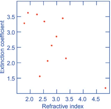
2901 nm. Four of the 15 nominally different solutions had coatings on two sides of the substrate. There were two solutions that employed two absorbing lay-ers: In one both layers were on the same side and in the other on the opposite sides of the substrate. The optical constants of the absorbing materials varied between 1.78 ⬍ n ⬍ 4.84 and 1.18 ⬍ k ⬍ 3.62 (see Fig. 6). As predicted in Section 3, none of the optical constants used were close to those of good reflectors such as Ag and Au.
The construction parameters of the 15 layer sys-tems depicted in column 1 of Fig. 4 are all very dif-ferent, and hence it is not surprising that there are significant differences between their transmittance and reflectance curves. And yet, it will be seen from Fig. 5 and Table 4 that a significant number of the filters have x and y CIE coordinates that are quite close to the specified target values. This subset of filters, when illuminated by the CIE Standard Illu-minant D65 at an angle of 7°, exhibit a triple metamerism in which all the samples appear to have the same or similar color not only in the transmitted light, but also in the light beams reflected from their two sides.
Good color photographs of optical thin-film inter-ference coatings are difficult to make because of the specular reflectance and the fact that the results de-pend on the illumination level and the angle of inci-dence of the light. Just for orientation purposes, in Fig. 7 are shown color photographs of the
near-Fig. 6. (Color online) Optical constants of the absorbing materials used in the Manufacturing Problem.
Fig. 7. Photographs of the (a), (b) reflected and (c) transmitted beams of a typical sample. (d) View of all three beams. See the text for more details.
normal appearance of the blue [Fig. 7(a)] and yellow [Fig. 7(b)] reflected and the transmitted [Fig. 7(c)] beams of a typical sample submitted. Figure 7(d) is an attempt to show the transmitted beam and the beams reflected by the two surfaces of the sample in one photograph. The color chart 1 and a mirror 2 rest against a white cardboard 3 that is illuminated by an extended light source. The sample 4 is held at some distance from this plane and is tilted in such a way that, in addition to the yellow front surface reflection
Ry, a blue reflection Rbof the second surface can be
seen in the mirror. The transmitted beam T falls onto the white cardboard. However, the colors of the three beams are not as specified: To obtain this view, the angles of incidence had to depart from the specified 7°. Furthermore, the white light falling onto the card-board desaturates the transmitted and the yellow reflected beams.
In view of the good agreement between the spectral transmittance and reflectance curves measured at NIST and ODA, it is not surprising that there is also good agreement between the merit function values derived from these measurements—the rms devia-tion of the normalized differences in the measured merit function values was of the order of 0.013. One would have expected the measured average merit function values to be higher than the theoretical
val-ues, and this of course was the case. The ratio of the average measured to the theoretical merit function values varied between 1.03 and 2.04, and for the highest ranking solution JZI it was 1.33. Somewhat puzzling were the ratios 1.03, 1.04 for the solutions UOM and RGO— either the control of the process of both thicknesses and optical constants of the absorb-ing materials was exceptional or the merit function values submitted were not the theoretical values but were based on measurements of the reflectances and transmittances at the manufacturing sites.
There is no obvious correlation between the num-ber of layers or the overall thickness of the layer systems and the theoretical values of the merit func-tion. This is probably due in part to the fact that the various participants used different sets of coating materials. One would especially expect the choice of the absorbing layers to have a marked effect on the resulting merit function values.
The Manufacturing Problem team (Fig. 8) thanks Edmund Optics for donating the substrates that were used in this year’s exercise. We are also grateful to David Allen, who performed most of the measure-ments at NIST; to Joanne Zwinkels, Michael Tru-betskov, and Markus Tilsch, who provided advice or comments on colorimetric aspects; to Geoff Aers,
Fig. 8. Manufacturing Problem team: standing from left to right are Maria Nadal, who unfortunately could not attend the OIC meeting; Michael Jacobson; Stephen Browning; and George Dobrowolski.
James Gupta, and Yanen Guo for help during the writing of the evaluation program; and to Harry Turner who took the color photographs of the typical sample.
References
1. J. A. Dobrowolski, S. Browning, M. Jacobson, and M. Nadal, “Topical meeting on optical interference coatings (OIC’ 2001): manufacturing problem,” Appl. Opt. 41, 3039 –3052 (2002). 2. J. A. Dobrowolski, S. Browning, M. R. Jacobson, and M. Nadal,
“2004 Optical Society of America’s Topical Meeting on Optical Interference Coatings: manufacturing problem,” Appl. Opt. 45, 1303–1311 (2006).
3. American Society for Testing and Materials, “Standard prac-tice for computing the colors of objects by using the CIE sys-tem,” ASTM Publication E308 (ASTM, 2001).
4. CIE, “Colorimetry,” 3rd ed., CIE Publication 15 (CIE, 2004). 5. F. Goos, “Durchlässigkeit und Reflexionsvermögen dünner
Silberschichten von Ultrarot bis Ultraviolett,” Z. Physik 100, 95–112 (1936).
6. H. Pohlack, “Über einige neuere Probleme der Grenzflächen-optik absorbierender Medien,” in Optik Aller Wellenlängen, P. Görlich, ed. (Akademie-Verlag, 1959), pp. 369 –373.
7. B. T. Sullivan and K. L. Byrt, “Metal兾dielectric transmission
interference filters with low reflectance. 2. Experimental re-sults,” Appl. Opt. 34, 5684 –5694 (1995).
8. D. Poitras, J. A. Dobrowolski, T. Cassidy, C. Midwinter, and C. T. McElroy, “Black layer coatings for the lithographic man-ufacture of diffraction gratings,” Appl. Opt. 41, 3306 –3311 (2002).
9. B. Badoil, F. Lemarchand, M. Cathelinaud, and M. Lequime, “An error compensation strategy for broadband optical moni-toring,” in Optical Interference Coatings on CD-ROM (Optical Society of America, 2007), presentation WC5.
10. M. Tilsch, “Optical Interference Coatings Design Contest 2007: triple bandpass filter and nonpolarizing beam splitter,” Appl. Opt. 47, C55–C69 (2008).
11. B. T. Sullivan, G. Clarke, T. Akiyama, N. Osborne, M. Ranger, J. A. Dobrowolski, L. Howe, A. Matsumoto, Y. Song, and K. Kikuchi, “High-rate automated deposition system for the man-ufacture of complex multilayer coatings,” Appl. Opt. 39, 157– 167 (2000).
12. B. T. Sullivan and J. A. Dobrowolski, “Implementation of a numerical needle method for thin-film design,” Appl. Opt. 35, 5484 –5492 (1996).
13. S. Sullivan, M. Tilsch, and F. Van Milligen, “Bigger is not always better in optical coating production,” Photonics Spectra 39(11), 86–92 (2005); see also http://www.jdsu.com/site/jdsu_public_ website/assets/pdf/JDSU_Optical_Films_Reprint_Final.pdf.