A Common Platform for Current Sensor Evaluation
in Industrial Automation Applications
by
Michael A. Wu
Submitted to the Department of Electrical Engineering and Computer
Science
in partial fulfillment of the requirements for the degree of
Masters of Engineering in Electrical Engineering and Computer Science
at the
MASSACHUSETTS INSTITUTE OF TECHNOLOGY
February 2016
c
○
Massachusetts Institute of Technology 2016. All rights reserved.
Author . . . .
Department of Electrical Engineering and Computer Science
January 15, 2016
Certified by. . . .
Ruonan Han
Professor of Electrical Engineering and Computer Science
Thesis Supervisor
Certified by. . . .
Siddharth Sundar
Design Manager, Silicon Laboratories, Inc.
Thesis Supervisor
Accepted by . . . .
Dr. Christopher Terman
Chairman, Masters of Engineering Thesis Committee
A Common Platform for Current Sensor Evaluation in
Industrial Automation Applications
by
Michael A. Wu
Submitted to the Department of Electrical Engineering and Computer Science on January 15, 2016, in partial fulfillment of the
requirements for the degree of
Masters of Engineering in Electrical Engineering and Computer Science
Abstract
This thesis describes the design and implementation of an evaluation system for Sil-icon Labs’ current sensor products. The system provides significant advantages over existing evaluation systems by reducing hazardous voltages and currents through in-creased sense resistance and improving simplicity through a modular motherboard, daughtercard, and software system. The system is versatile and supports modifica-tions for additional customization. All existing Silicon Labs’ current sensor products are implemented in the system. The performance of the constructed evaluation sys-tem is shown to exceed existing work. The constructed syssys-tem uses lower currents, requires fewer specialized components, improves portability, and provides access to advanced product functionality.
Thesis Supervisor: Ruonan Han
Title: Professor of Electrical Engineering and Computer Science Thesis Supervisor: Siddharth Sundar
Acknowledgments
The completion of this thesis would not have been possible without the help of many. I would like to thank Ariel Rodriguez for his help in developing the concept of this thesis and his patient guidance throughout the process. I am grateful to my adviser, Sid Sundar, not only for his advice on my thesis but also on life and careers in general. Engineers from the Isolation group made me feel welcome at Silicon Labs, and were always available for help. I have relied numerous times on help from Keith Coffey and Jason Webb for schematic reviews and circuit advice.
At MIT, I would like to thank Professor Han. Professor Han provided helpful guidance throughout the project proposal and thesis.
Finally, I would like to thank my family - my sister and my parents, for keeping me sane and motivated through the process.
Contents
1 Introduction 13
1.1 Motivation for an Evaluation Module . . . 13
1.2 Thesis Objectives and Approach . . . 14
2 Background 15 2.1 Current Sensing Topology Review . . . 15
2.1.1 Sense Resistor Current Sensing . . . 15
2.1.2 Rogowski Coil Current Sensing . . . 17
2.2 Silicon Labs Current Sensing Overview . . . 18
2.2.1 Si85xx: Unidirectional AC Current Sensor . . . 18
2.2.2 Si8540: High-Side Current Sense Amplifier . . . 19
2.2.3 Si890x: Isolated ADC . . . 19
2.2.4 Si892x: Isolated Differential Amplifier. . . 20
2.3 Silicon Labs Current Sensing Evaluation Boards . . . 20
2.3.1 Si85xx-EVB . . . 21 2.3.2 Si890x-PWR-EVB . . . 22 2.3.3 Open-Loop-POL . . . 24 2.4 Proposed Implementation . . . 26 3 Motherboard Design 27 3.1 Power . . . 29 3.2 Signal Generation . . . 30 3.3 Current Amplifier . . . 34
3.4 Buck Load . . . 36 3.5 Measurement System . . . 38 3.6 Summary . . . 39 4 Daughtercard Design 41 4.1 Si8540-DC . . . 43 4.2 Si85xx-DC . . . 44 4.3 Si890x-DC . . . 44 4.4 Si892x-DC . . . 46 4.5 Summary . . . 46 5 PC Software Design 47 5.1 Communication Scheme . . . 47 5.2 Software Architecture . . . 48 5.3 User Interface . . . 48 5.4 Summary . . . 49 6 System Performance 51 6.1 Low Voltage and Current. . . 52
6.2 Minimal External Components. . . 52
6.3 Simplicity . . . 53
7 Conclusion 55 7.1 Summary . . . 55
7.2 Future Work . . . 55
7.2.1 High Frequency Measurements. . . 55
List of Figures
2-1 Sense resistor current sensing topology. . . 16
2-2 Rogowski coil current sensing topology. . . 18
2-3 The three versions of the Si85xx-EVB. . . 21
2-4 Block diagram of the Si890x-PWR-EVB. . . 23
2-5 Photo of the Si890x-PWR-EVB and its associated cover and connectors. 24 2-6 Photo of the Open-Loop-POL EVB . . . 25
2-7 High level architecture of the proposed implementation. . . 26
3-1 Motherboard high level architecture . . . 27
3-2 Photo of the current sense motherboard. . . 28
3-3 Architecture of direct digital synthesis . . . 31
3-4 Phase wheel concept in direct digital synthesis . . . 31
3-5 Example output of the signal generator. . . 34
3-6 Schematic of the current amplifier . . . 35
3-7 Input/output characteristic of the current amplifier. . . 35
3-8 High side switch current of the buck load as measured by a Si85xx. . 37
3-9 Examples of the output of the measurement system and the advance controls it offers. . . 40
4-1 Photo of the Si892x daughtercard . . . 41
4-2 Motherboard measurements system requesting ADC data from the Si8900 over UART. . . 45
List of Tables
2.1 Summary of various current sensor topologies. . . 15
2.2 Summary of Silicon Labs’ current sensing portfolio. . . 18
2.3 Summary of existing EVM characteristics. . . 21
3.1 Current budget of the major components of the motherboard. . . 29
4.1 Motherboard-Daughtercard connector pin assignment . . . 42
6.1 Summary of voltage and current for evaluation systems. . . 52
6.2 Summary of external components required for evaluation systems. . . 53
Chapter 1
Introduction
1.1 Motivation for an Evaluation Module
Evaluation modules are an essential product used in the marketing and sales of in-tegrated circuits (ICs). Before purchasing large quantities of products, customers need to be able to accurately assess the electrical characteristics of a device and un-derstand exactly how it interacts with other components of a system. Evaluation platforms enable customers to quickly develop new products, incorporating complex semiconductor designs, by providing circuitry that demonstrates the capabilities of a IC. In order to assist customers in their endeavors, it is essential that an evaluation platform accurately demonstrates a product’s features and enable evaluation, while minimizing complex setup and provide a simple interface.
Industrial current sensing presents unique challenges to the development of an evaluation module due to the high currents and power. Measured currents in indus-trial settings can often be on the order of 1-10 A. There are significant challenges in the generation of sizable input signals and management of high voltage, current and heat. Previous current evaluation boards at Silicon Labs required complex setup, used hazardous voltages and currents, and provided a non intuitive method for evaluating products.
1.2 Thesis Objectives and Approach
The goal of this thesis is to improve industrial grade current sensing by creating a sim-pler and safer evaluation platform. This work was performed at Silicon Labs, a leader in the innovation of high performance, analog intensive, mixed-signal semiconductors. The organization of this thesis is as follows: Chapter 2 overviews background knowledge relevant to current sensing and evaluation modules. Chapter 3 covers the motherboard circuit design and implementation. The proposed evaluation board is introduced. Chapter 4 covers the design of and implementation of daughtercards as-sociated with the platform. Chapter 5 covers design of the final component of the evaluation system, the evaluation measurement software. Chapter 6 presents the re-sults of circuit performance. The system’s ability to evaluate products through signal generation and measurement is tested. Comparisons to the safety and complexity of previous evaluation platforms are analyzed. Chapter 7 concludes with a summary of this work and suggestions for future work.
Chapter 2
Background
2.1 Current Sensing Topology Review
There are a number of topologies used to measure a current, each with their own ad-vantages and disadad-vantages. Understanding the intricacies of each topology informs the design of signal generation and measurement systems associated with each sensing topology. A brief summary of several characteristics of common current sensing tech-niques is presented inTable 2.1. This section reviews sense resistor and Rogowski coil current sensing, which are topologies used in Silicon Labs’ current sensing portfolio.
Toplogy Resistance (mΩ) Bandwidth (kHz) Accuracy (±%)
Sense Resistor 10 DC - 200 5
Rogowski Coil 1 50-1,000 5
Hall Effect None DC - 300 10 - 30
Current Transformers 6 - 20 50 - 1,000 15
Table 2.1: Summary of various current sensor topologies.
2.1.1 Sense Resistor Current Sensing
Sense resistor current sensing is a form of direct measurement where a resistor is placed in series with the current load. The topology is presented in Figure 2-1.
This circuit is premised on Ohm’s Law. Given a known resistance and a measure-ment of the differential resistor voltage, it is possible to calculate the current through
𝐼 ∆𝑉 = 𝐼𝑅 − + 𝑉+ 𝑉− 𝑉𝑜
Figure 2-1: Sense resistor current sensing topology. the resistor as shown in Equation 2.1.
𝐼 = ∆𝑉
𝑅 (2.1)
In practice, the sense resistor is designed to have a low resistance to minimize the power dissipated. In industrial settings, where currents can be tens of Amperes, thermal dissipation can exceed 1 W, which must be appropriately cooled to prevent increasing system temperature. Resistor values on the order of 10 mΩ are common.
By decreasing the sense resistance, the thermal dissipation can be reduced, how-ever the differential voltage across the sense resistor is also reduced. This presents issues when using the differential voltage as input to another system as the signal is compressed into a small voltage interval. Typically, the resistor voltage is amplified to present a signal of sizable amplitude to other components.
In implementation, there exists a maximum differential voltage across the ampli-fier inputs where the gain is linear due to the limited input or output range of the amplifier. This maximum differential voltage is designed to correspond to a full scale output voltage of the amplifier. Thus the overall transfer function of the topology can be given by
𝑉𝑜
𝐼 = 𝑅
𝑉fullscale
𝑉input,max (2.2)
and amplification. It is a direct form of measurement which affects the current load and dissipates power. Defining characteristics of sense resistor products are their dif-ferential amplifier properties such as bandwidth, input offset voltage, and input/out-put full-scale voltages.
2.1.2 Rogowski Coil Current Sensing
Rogowski coils are are circuit that allows for the indirect measurement of current through magnetic fields associated with the current. A coil is circularly wrapped around the current signal of interest. The operation of this circuit is premised on Ampere’s Law of Induction [16]. Ampere’s Law is a statement that the path integral of the magnetic field 𝐵 enclosed by loop 𝐶 is the current 𝐼 enclosed by the path. For a coil, this reduces to the following.
𝐵 = 𝜇0𝐼
2𝜋𝑟 (2.3)
We can derive the voltage of the inductive coil in response to a current as shown below in Equation 2.4. Observe that the derived equation takes the form of the constituent relation of an inductor. Thus we can model a Rogowski coil as a pair of coupled inductors. 𝑉𝐿= −𝑁 𝑑𝜑 𝑑𝑡 = − 𝑁 𝐴𝜇0 2𝜋𝑟 𝑑𝐼 𝑑𝑡 = −𝐿 𝑑𝐼 𝑑𝑡 (2.4)
We see that the voltage across the coil is proportional to the derivative of cur-rent. By integrating the voltage through the coil, we can measure a signal that is proportional to the current. This final topology is shown in Figure 2-2.
Inaccuracies are introduced into the system due to the limited precision of compo-nents and nonideality of the integrator. These errors will accumulate with unbounded time integration and can lead to sensitivity to DC offset errors. To provided an upper bound on measurement error, Rogowski coils are often designed to periodically reset the output voltage and restart the measurement cycle.
𝐼
𝑉𝐿= 𝐿𝑑𝑖𝑑𝑡
∫︀ 𝑉𝐿𝑑𝑡
𝑉𝑜
Figure 2-2: Rogowski coil current sensing topology.
upon coupled inductance. The output voltage is proportional to the measured current. The integration inherent to this measurement scheme restricts the minimum operating frequency and necessitates a reset period during each measurement cycle.
2.2 Silicon Labs Current Sensing Overview
Silicon Labs produces four families of current sensor products, each optimized for different applications and needs. This section briefly reviews the functionality and underlying technology to inform design decisions of a current sensor evaluation plat-form. A summary table is provided below in Table 2.2.
Product Topology Description Frequency (kHz)
Si85xx Rogowski Unidirectional AC Sensor 50 − 1, 000 Si8540 Sense Resistor High Side Amplifier 0 − 20 Si890x Sense Resistor Isolated Serial ADC 0 − 125 Si892x Sense Resistor Isolated Differential Amplifier 0 − 1, 000
Table 2.2: Summary of Silicon Labs’ current sensing portfolio.
2.2.1 Si85xx: Unidirectional AC Current Sensor
The Si85xx product family is a current sensor IC sold by Silicon Labs which is an implementation of a Rogowski coil [6]. As reviewed in the Rogowski Coil overview, the topology requires a minimum frequency and a reset period during each measurement
interval. The frequency characteristics are provided in Table 2.2. Due to the use of a Rogowski coil, the Si85xx is electrically isolated between the current load and output signal.
More relevant to the evaluation system design are the full scale currents of the products. The Si85xx family has a 2 V output voltage, corresponding to either a 5 A, 10 A, or 20 A input current depending on the specific product. This will present a challenge when trying to minimize the current in the evaluation module.
2.2.2 Si8540: High-Side Current Sense Amplifier
The Si8540 is an amplifier that fits within the sense resistor topology [12]. The device is designed to be placed in a high side configuration, where the sense resistor is placed between the load and the positive supply. The advantage with high side sensing is that the load is connected to ground and not floating due to a sense resistor [3]. The Si8540 is powered by drawing current from its inputs. This requires a minimum common mode voltage of 5 V on the input pins. As explained in the review of sense resistor topologies, the current sense amplifiers have a maximum input referred differential voltage. For the Si8540, the maximum differential input voltage is ±0.3 V.
2.2.3 Si890x: Isolated ADC
The Si890x product family is a series of isolated analog to digital converters (ADC) with serial output [10]. The ADC has a resolution of 10 bits and maximum sampling frequency of 500 kHz. The Si890x provides the digital value to a MCU through serial communication over UART, I2C or SPI. Depending on the serial communication clock frequency, the effective sampling rate will be further throttled by the communication rate. The Si890x provides an isolation barrier between the analog input and digital output through Silicon Labs patented CMOS isolation barrier.
Though the Si890x products are general purpose ADCs, they are marketed to-wards high voltage and high current signal monitoring, with an emphasis on AC line monitoring. Isolation is a desirable property to protect a MCU from the high current
signals and analog to digital conversion is useful as more logic is moved into the digital domain.
Speaking more towards the current sensing aspect, note that the Si890x is not an amplifier and requires a separate IC to appropriately condition the current signal to the Si890x input range. Though the Si890x requires an additional IC for current sens-ing, it provides additional functionality in the form of programmable gain, multiple ADC channels, and configurable continuous measurements. With regard to inputs, the Si890x family uses a full scale input voltage of 3.3 V.
2.2.4 Si892x: Isolated Differential Amplifier
The Si892x product family is a series of isolated differential amplifiers with fully differential output [14]. This differential amplifier uses Silicon Labs patented CMOS isolation barrier to provide electrical isolation between input and output, making it desirable for current sensing.
With regard to current sensing, the Si892x fits within the sense resistor topology. It provides a fixed voltage gain of 8.1 or 16.2. It has a maximum input differential voltage of ±100 mV. This provides full scale output signals of 1.62 Vpp which is an appropriately sized signal to be used after current sensing.
2.3 Silicon Labs Current Sensing Evaluation Boards
Semiconductor companies typically sell an evaluation module (EVM) to demonstrate a product’s capabilities to customers. Prior to discussing the design of the a common EVM for current sensing, we first review the existing evaluation modules at Silicon Labs. At the time of this project, Silicon Labs had three evaluation platforms, which covered the Si85xx, Si8540 and Si890x product families. The strengths and areas for improvement for each of these platforms will be discussed in the remainder of this section as they form the basis for the design of the proposed evaluation platform. A summary of relevant characteristics is provided below in Table 2.3, with subsequent sections going into specific details.
Product Max Current ComponentsExternal
Si85xx-EVB 5 A 4
Si890x-PWR-EVB 10 A 3
Open-Loop-POL-EVB 10 A 5
Table 2.3: Summary of existing EVM characteristics.
2.3.1 Si85xx-EVB
The Si85xx-EVB is the evaluation module for the Si85xx Unidirectional AC Current Sensor [8]. Three versions of the EVB are sold corresponding to the 5 A, 10 A, and 20 Aversions of the Si85xx. A picture of these evaluation boards is shown inFigure
2-3. The Si85xx-EVB acts as a breakout board for the Si85xx ICs. Located at the south end of the board are turrets labeled I_IN and I_OUT. These turrets are used to provide a high current path for the input current through the device. Directly north of the input turrets is the Si85xx IC, labeled as U1. Further north of the IC are header pins, which provide access to the pins of the IC. At the north end of the board are turrets labeled for power. Overall, the Si85xx-EVB is a minimal cost evaluation board that provides access to pins through header pins and turrets as opposed to QFN pins.
Figure 2-3: The three versions of the Si85xx-EVB.
The Si85xx-EVB is acceptable if the customer has an existing system capable of generating high current. However, if the customer does not have a pre-existing
system, it can be difficult to generate AC currents in the 5 A, and > 50 kHz range of the Si85xx. This would typically require building an amplification system to evaluate the product. This can be a time consuming endeavor which hinders the usefulness of the evaluation board.
Furthermore, the Si85xx-EVB does not provide a simple interface for measuring or inputting signals. The Si85xx requires a minimum of two logic signals to periodically reset the current integration. The header pin interface does not provide a simple connection. Connecting wires directly to the header pins increases the chances of accidentally shorting signals. Attaching a cable connector will lead to the same issue on the other end of the cable, unless a separate board is designed to provide neatly route the signals to the cable. In short, the input / output interface of the Si85xx-EVB greatly hinders a customer’s ability to actually use the board unless they invest additional time in constructing additional cabling and boards.
In evaluating the simplicity of the board, we look at additional external equip-ment necessary for operation. The EVM requires, at minimum, a power supply and oscilloscope to measure the output. A high frequency, current source and a signal generator for reset timing are also required. While a power supply, oscilloscope and signal generator are standard in most lab environment, the high frequency high cur-rent source stands out as a component that would be more unusual to have lying around. In summary, the Si85xx-EVB requires high currents, significant setup and many pieces of additional equipment.
2.3.2 Si890x-PWR-EVB
The Si890x-PWR-EVB is the evaluation module for the Si890x Isolated Monitoring ADC. This EVB is meant to serve as a reference design for using the Si890x products to monitor the voltage and current draw of a device on the AC mains. A block diagram of the Si890x-PWR-EVB can be seen inFigure 2-4.
The AC line is measured on the right hand side of the board. Voltage and current are measured using the Line and Load inputs on the high voltage side of the board. Note that the current sense voltages must be appropriately scaled by amplifiers to
Figure 2-4: Block diagram of the Si890x-PWR-EVB.
match the specified input range of the Si890x. Here, in the amplifiers, lies one of the issues with the Si890x-PWR-EVB. As the board was designed to be a reference design for the AC Mains, the amplifiers are appropriately designed to scale signals typical of the AC Mains to the input range of the Si890x. The amplifiers are designed to have a current gain of 0.054 V/A and voltage gain of 0.004 [4]. These attenuators cannot be bypassed without modification to the board. The Si890x EVB User Guide recom-mends attaching this EVB to the AC line. While the product is appropriately rated to handle such conditions, it does incur a safety risk for engineers who use this device to evaluate the Si890x [11]. Silicon Labs recognizes this risk and therefore requires the use of a protective cover during operation of the device as shown in Figure 2-5. While this mitigates some risk, it also inhibits troubleshooting or observation during the operation of the device, which is crucial during the evaluation of a product.
Aside from the preset amplifier gains, the Si890x-PWR-EVB presents another challenge for evaluation in the current and load that it requires. As explained above the EVB requires significant voltage and current to demonstrate an appreciable signal output. The user guide recommends the use of a power resistor that can safely handle up to 10 A of current. Not only is this a sizable power resistor, but it also means that the user will only be able to test fixed amplitude signals unless they obtain multiple
Figure 2-5: Photo of the Si890x-PWR-EVB and its associated cover and connectors. values of power resistors. There are a number of challenges with the high power side of this evaluation board including preset gains necessitating large input voltage and current as well as large recommended loads and a lack of flexibility of inputs.
The output side has its own share of issues as well. The output connector itself is a non-standard 3x3 header pin. The user guide recommends soldering 9 wires to a male header connector; this is more challenging than it sounds. A simpler output scheme, such as probe loops would reduce the difficultly of accessing measurements.
The firmware of this board also provides challenges. As the Si890x devices output values over UART/I2C/SPI, the board provides a MCU to perform of communication. This MCU defaults to a specific clock frequency and feature set. In order to evaluate the product across varying conditions and using other features, the customer must request the source code, compile it, and flash it to the MCU. This represents a significant effort for someone who simply wants to evaluate the product.
2.3.3 Open-Loop-POL
The last evaluation platform from Silicon Labs is the Open-Loop-POL. The POL stands for Point of Load and implements a basic DC to DC down converter. Of the
Figure 2-6: Photo of the Open-Loop-POL EVB
three evaluation platforms sold, this board is the most developed. The Open-Loop-POL uses the Si85xx to measure the high frequency switch current and the Si8540 to measure the output current of the buck converter. A picture of the Open-Loop-POL can be seen in Figure 2-6.
The Open-Loop-POL is a good example of an evaluation system because it simpli-fies the evaluation process by providing associated circuitry necessary for operating the device. As explained for the Si85xx-EVB, high frequency high current signals are difficult to generate in a lab without a pre-existing system. Furthermore, it al-lows the customer to configure device timings and features through convenient BNC connectors and jumper pins.
While the Open-Loop-POL does provide access to a number of features, there are still several areas where it can be improved. The board expects a significant current, up to 10 A from its power supply. The load of the buck converter is expected to be rated for 10 A. The user guide recommends using a high power digital load to control the current [7]. Such a digital load would most likely not be found in most laboratory environments. Furthermore, the Open-Loop-POL requires many pieces of equipment for operation. Multiple power supplies, high power digital load, signal generator and multiple oscilloscope channels are necessary for operation. While many components are standard in a lab, reducing the number of required components would simplify the evaluation process and reduce setup time.
2.4 Proposed Implementation
In reviewing the set of existing current sensor evaluation platforms, we determine there are multiple areas for improvement, such as high current/power requirements, lack of functionality/simplicity and safety concerns. Furthermore, each product fam-ily is separately supported by a different evaluation platform and there is no common evaluation metric for the various products.
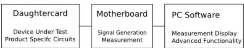
To solve these issues, we proposed a unified evaluation system that supports all of Silicon Labs current sensors products. The evaluation system consists of a moth-erboard, daughtercard and PC software. The motherboard would contain common circuitry necessary for the evaluation of all products, such as power, signal genera-tion and output signal measurement. The daughtercards would implement product specific circuitry such as necessary signal conditioning. Lastly, we aim to provide a software interface to simplify testing advanced functionality and measuring output signals. A high level architecture of this design in shown in Figure 2-7.
Figure 2-7: High level architecture of the proposed implementation.
The goals of the proposed implementation are to provide a safer and simpler unified current evaluation platform by reducing the maximum current and voltage on board and providing default circuitry on the evaluation module to assist the user in evaluation. Reducing the maximum current will be achieved by increasing the sense resistance to provide equivalent sense voltage for a lower current. Default circuitry will consist of signal generation and measurements systems connected to PC software to enable users to quickly perform measurements, vary inputs, and test advanced features of the Silicon Labs current sensors. The remainder of this thesis document will detail the design and results of the motherboard, daughtercard and PC software modules.
Chapter 3
Motherboard Design
At the core of the implemented work is the current sense motherboard, which unifies the evaluation of all Silicon Labs current sensors by providing a common platform for evaluation. Specifically, the motherboard provides circuit modules for power, current signal generation and output signal measurement. These modules were found to be circuits that would be typically implemented for each evaluation module and by providing a generic interface on the motherboard, we reduced duplicated circuits. A brief overview of the motherboard is initially provided and the remainder of this chapter details the design of the current sensor motherboard.
Figure 3-1: Motherboard high level architecture
The high level architecture for the motherboard is presented in Figure 3-1. As explained previously, the motherboard contains the necessary modules for generating
input and measuring output of any current sensor device. Inputs waveforms are generated, then passed to two types of loads, either a current amplifier or a buck load. The outputs of the loads then go on to the current sensor. The output of the sensor returns to the motherboard as either an analog signal or as digital serial communication. These output signals are processed by an on-board MCU and then passed to PC software for display and additional analysis. The final realization of the motherboard is shown in Figure 3-2.
Figure 3-2: Photo of the current sense motherboard.
On the motherboard shown in Figure 3-2, the signal generator is on the left hand side and the measurement system is on the right hand side. The potentiometers labeled FREQ and DUTY are controls for the signal generator. Most of the actual circuitry is on the bottom of the board. On the right hand side of the board is a USB connector. This is how the motherboard connects to the PC. Finally, at the bottom of the board are header pins in a box labeled DAUGHTERCARD. These pins are how the daughtercard connects to the motherboard.
3.1 Power
The goal of the power module is to provide adequate power for the evaluation of products while also minimizing the current and voltage to prevent hazardous condi-tions. This section details the design of the power module on motherboard. There are multiple modules that require various levels of voltage and current. An analysis of current consumption is presented inTable 3.1. As indicated in the table, 3.3 V and 5 V are required for the operation of various MCUs and controllers. These voltages are simply generated using linear regulators. Significant power draw is not expect to flow through these channels, thus the efficiency drop of linear regulators is acceptable. The main design decision is how to set the input voltage and current such that the signal generator and buck load will be able to function while also minimizing the maximum voltage and current.
Subsystem Required Current Additional Notes
Waveform Generator MCU 10 mA 3.3 V
Current Amplifier 100 mA
Buck Load Control 10 mA 5 V
Measurement MCU 30 mA 3.3 V
Maximum Daughtercard 20 mA > 5 V for Si8540
Sum 170 mA 3.3 V, 5 V
Table 3.1: Current budget of the major components of the motherboard.
In order to minimize the current consumption of the current amplifier, the re-sistance of the sensor resistor for the DUTs were increased. This allowed for near full-scale outputs of the sensors with an input of 100 mA. The design and implica-tions of this decision will be further explained in section 3.2 on signal generation. This level of current was chosen because it significantly reduced the current level compared to existing evaluation boards, thereby increasing safety. The input voltage was chosen to be 9 V. This voltage was chosen based upon the minimum required voltage for modules and availability of the output voltage of AC wall adapters.
Power can be provided to the motherboard through either an AC wall adapter or through a regular lab power supply. The included AC wall adapter provides 9 V
output at a maximum of 1.7 A. Using a wall adapter enables the motherboard to be used outside of a lab environment, such as while demonstrating products to customers in the field. The maximum current of the adapter provides sufficient current for low current signal generator and higher current buck load.
Alternatively, it is understandable that customers may want to evaluate the system at significantly higher currents. Banana plugs are provided to connect to standard power supplies. This allows the user to increase the current provided to the buck load and evaluate the system at higher currents. Peak DC current should be limited to less than 2 A due to the connectors used on the motherboard. For evaluation under higher current loads, the daughtercard can be used without the motherboard, allowing for currents up to 5 A.
The power module supports a diverse set of modules at various voltage and current levels. Input current and voltage levels were chosen to support DUT evaluation and minimize hazardous conditions. Power is supplied through either a supplied AC wall adapter or a standard lab power supply. Voltage is regulated down as necessary for digital components.
3.2 Signal Generation
In order to evaluate a product, a known input signal must be generated to stimulate the device. To properly test Silicon Labs current sensors, a module must be capable of generating signals from DC to hundreds of kilohertz. It should be able to drive analog circuitry directly and also generate logic waveforms for the buck load. To meet these challenges, it was decided that a digital system would have more flexibility to meet the specifications over an analog oscillator. In addition, a digital generator had pre-built modules for pulse width modulation (PWM) which would simplify the generation for the buck load. Analog oscillators were considered, but ultimately found to have limited ability to span the wide frequency range of interest with appropriate resolution. Furthermore, the digital implementation provided additional flexibility by being able to generate generic periodic waveforms, while analog implementations
typically targeted only sine waves. The specific implementation was chosen to be direct digital synthesis, due to its excellent frequency resolution over our range of interest [1].
Figure 3-3: Architecture of direct digital synthesis
Prior to explaining the implementation, a brief review of direct digital synthesis is discussed. The system architecture is shown in Figure 3-3. A periodic waveform is stored in digital memory and can be accessed through a lookup table. At a given time, we can describe the position within a periodic waveform using the phase of the signal. On each cycle of the system clock, the phase of the system is increased by a set amount, known as the phase step. The phase is used to lookup the corresponding stored value in memory. The digital value is finally converted to an analog signal using a digital to analog converter and low pass filter.
The power of direct digital synthesis is that it allows for arbitrary output frequen-cies by modifying the phase step taken on each cycle of the system clock. Consider the example provided in Figure 3-4. Shown are 16 samples of a periodic waveform. The angle from the x-axis represents the phase of the system. Normally, we incre-ment the phase by one on each clock cycle. With N points, this leads to an output frequency of 𝑓out = 𝑓2𝑐𝑙𝑘𝑁 . Now consider if, on each clock cycle, the phase moves half
of a sample. This doubles the amount of time to traverse the waveform and halves the output frequency. Specifically, if phaseStep represents the size of the phase step in samples, we can write the following.
𝑓out = 𝑓𝑐𝑙𝑘 *phaseStep
2𝑁 (3.1)
By controlling the phase step, we can achieve arbitrary output frequencies. If the phase accumulator contains a fractional value that does not correspond to a sample, the phase will be truncated to the last available sample. If the system is operating at a frequency significantly higher than the output frequency, the low pass filter at the end of the output will correctly interpolate the signal.
Fractional phase steps are efficiently implemented using additional fixed point reg-isters. Given 2𝑁 samples, the phase can be represented with a N-length bit string.
We can represent the fractional portion by adding another 𝐹 bits to the least signif-icant end of the phase. Simple addition will now correctly and efficiently track the fractional phase. To extract the index to lookup sample values, the top 𝑁 bits are simply extracted.
The implementation of this module is now discussed. Silicon Labs’ C8051F390 was chosen as the micro-controller to implement direct digital synthesis. The C8051F390 is a 8-bit, low cost micro-controller based on the Intel 8051 architecture. This device was chosen due to built-in functionality as it has a high system clock rate, built-in current DAC, low cost and size. Given the 8-bit architecture, we chose to implement 8-bit lookup tables with 256 samples for the periodic waveforms. The phase accumulator was 16-bits, with the most significant 8 bits corresponding to the phase lookup table.
One challenge was efficiently implementing direct digital synthesis in software. The noise in the output signal is dependent upon the system clock frequency being significantly higher than the cutoff of the final low pass filter. Furthermore, the timing between phase steps must be precise to maintain a consistent frequency. The system clock frequency has several tradeoffs. The maximum frequency is constrained by the amount of time required to add the phase, lookup the sample value, and write the sample to the digital to analog converter. The minimum frequency is constrained by the maximum amount of quantization noise allowed in the output signal. Pushing the system frequency higher will increase the attenuation of the quantization noise by the low pass filter.
while (1) {
WaitFor (DAC Timer )
DAC = LookupTable [ PhaseIndex ] PhaseAccumulator += PhaseStep }
Code 3.1: Pseudo code of direct digital synthesis implementation.
Pseudo code for the implementation of direct digital synthesis is shown inCode 3.1. While most of it is straightforward, there are several subtle points. The logic waits until the sample period has finished and the DAC has outputted a value. The DAC in-terval value can now be overwritten to update the output value with the next sample. This advantage of this structure over an interrupt based structure is the guaranteed timing. For the specific implementation, as discussed above, the PhaseIndex is the top eight most significant bits of the PhaseAccumulator variable. Due to the align-ment of these variables with word boundaries in the 8-bit architecture, this can be efficiently extracted. The timing of this loop was found to be minimized at 52 machine cycles. This constrains the system to a system frequency of 49 MHz/52 = 942 kHz. The low pass filter was a first order low-pass filter with a break frequency placed at 𝑓−3dB = 390 kHz. These parameters provide sufficient filtering of the quantization
noise of the output. An example of the output of the signal generator is shown in
Figure 3-5. The yellow trace shows the output of the signal generator, while the blue trace shows the output of the current amplifier. The signal generator was configured to generate a sine wave with 8-bit resolution. As shown in the figure, the signal gen-erator is capable of producing waveforms sufficient for evaluating the current sensor products.
Figure 3-5: Example output of the signal generator.
3.3 Current Amplifier
The current amplifier is designed to amplify the output of the signal generator to appropriate levels for the current sensors. The implementation of the current amplifier is shown inFigure 3-6. The amplifier converts the output of the signal generator from peak to peak values of 2 Vpp, 2 mApp to 6 Vpp, 100 mApp.
This amplification is performed by a simple non-inverting op-amp amplifier and a designed output load. The op-amp amplifier has a voltage gain of 3, which appro-priately scales the voltage. The amplifier terminates in a designed 60 Ω load, which scales the current to 100 mVpp. The chosen op-amp saturates at 48 mA [15]. To allow the amplifier to drive a larger current, a bipolar junction transistor (BJT) is added at the output of the op-amp and the feedback is taken at the emitter of the BJT. The
Figure 3-6: Schematic of the current amplifier
transistor acts similar to a emitter follower, tracking the voltage at the input of the BJT. The feedback of the system corrects the non-linearity introduced by the BJT below the diode voltage. The linearity of the amplifier is shown in Figure 3-7.
Figure 3-7: Input/output characteristic of the current amplifier.
It should also be noted where the actual measurement occurs. In Figure 3-6, the sense resistor can be connected in series with either the collector or the emitter of the BJT. The difference between these two locations is the difference between high-side and low-high-side sensing. Both high-high-side and low-high-side sensing will have a current of
100 mApp, however the high-side resistor will have a differential measurement that is floating above ground. This distinction is important for current sensing applications, where referencing the load to ground can be important. This is further applicable to our system because the Si8540, the self powered differential amplifier, requires input above 5 V. By providing both high-side and low-side sensing, we provide the opportunity for the customer to evaluate the response of their systems under both circumstances.
3.4 Buck Load
The other current signal generating module in the motherboard is a buck converter. This module was included in the design because the signal generator and waveform amplifier do not have the current range or bandwidth to properly excite the Si85xx AC current sensor. Referring back to subsection 2.2.1, the Si85xx is a coupled inductor based sensor. Unlike the other sensors, we cannot increase a sense resistance to artificially increase the measured response. Furthermore, the Si85xx has a minimum input frequency of 50 kHz, which is above the frequency range of the signal generator [6].
A simple high frequency buck converter addresses both of these issues. The switch-ing frequency for this power converter was designed to be in the hundreds of kilohertz, and we can observe large amplitude ripple currents without drawing significant DC current. The design of this module is very similar to the Open-Loop-POL evaluation module (subsection 2.3.3), but lowers the necessary current to increase safety and also provides the signal generation circuitry to simplify the setup and measurement. While the details of dc to dc converters are beyond the scope of this document, the principal is that the converter rapidly switches the output between the input voltage and ground. Low passing filtering the output retains only the DC value. While switching between the input voltage and ground, we will be able to observe current transients at the switches as the output capacitor is charged and discharged. This ripple current is given by the following Equation 3.2 which is derived in [2]. 𝐷
represents the duty cycle of the PWM waveform, T is the period, 𝑉𝑖𝑛 is the input
voltage, and 𝐿 is the inductance of the inductor in the low pass filter.
∆𝐼𝑝𝑝=
𝐷(1 − 𝐷)𝑇 𝑉𝑖𝑛
𝐿 (3.2)
The key difference between the implementation of this module and the Open-Loop-POL is that this implementation, by default, is not connected to a load. The ripple characteristics of the switches are still visible to the Si85xx, but this eliminates the large DC current and the requirement for a sizable digital load. These were two of the issues with using the Open-Loop-POL.
Figure 3-8: High side switch current of the buck load as measured by a Si85xx.
This change further highlight the uni-directionality of the Si85xx. Due to the no load condition, the synchronous buck converter has reverse current flowing through the high side switch as the inductor maintains the current flow present during the low-side discharging portion. As such, the Si85xx will only measure current in the forward direction and thus this design highlights the uni-directionality [9]. This phenonenom can be seen in Figure 3-8. The bottom yellow trace represents the PWM signal on the gate of the high side switch. The top blue waveform is the measured signal from the Si85xx measuring the high side switch current. Note that the switch current does not begin to increase when the gate voltage is pulled high. This is because the
inductor current is flowing backwards through the body diode of the switch. When the inductor current reaches zero and begins forward flow through the Si85xx, the measured signal shows the appropriate response.
The control signals for the switches of the buck converter are generated by the signal generator. The generator provides a fixed frequency 192 kHz pulse width modu-lated output with variable duty cycle. The buck converter’s duty cycle is controllable through a potentiometer on the motherboard and can be adjusted between 0 to 80% duty cycle. As shown inEquation 3.2, the amplitude of the ripple will depend on the duty cycle and this provides a method through which the user can examine how the Si85xx responds to various amplitudes of current signals.
3.5 Measurement System
The last common module implemented on the motherboard is the measurement sys-tem to simplify the evaluation of products. By including a measurement syssys-tem, this makes the system more portable and allows the measurement system to interact with products with digital outputs, such as the Si890x products. This section will first discuss the design of the analog to digital measurements and then detail how serial digital communication was performed. Both of these systems are implemented on a single MCU, with built-in support for ADC measurements and serial communication. The goal of the analog measurement system is to perform analog to digital con-versions at an adequate sampling frequency to describe the output signal. As the ADC is built into the MCU, the only real design parameter is sampling method and the sampling frequency. The key issue with the sampling method is that results are continuously streamed to PC software for display and analysis. Sending data over USB to the PC requires instruction overhead, during which measurement is not pos-sible. Due to the lack of ability to communicate and measure in parallel, sending each measurement is woefully inefficient. The system therefore batches several thousand measurements to send as a group to minimize the effects of communication overhead. This is further discussed in section 5.1.
The sampling frequency was chosen to be the maximum sampling frequency of the ADC to maximize the highest frequency signal that could be measured. This MCU was constrained to 200 kilosamples / second. While other MCUs did have higher sampling rates, the choice of MCU was driven by having a well established code base for MCU to PC communication specifically tailored for this microcontroller. The maximum frequency for the signal generator was set to be 10 kHz, giving us a minimum of 20 samples per cycle. The limitation of the sampling frequency does mean that it is not possible to accurately measure the response of the buck converter which is operating at 192 kHz.
The other aspect of the measurement system is the digital communication module. The Si890x family of current sensors provides a digital output in the form of UART, I2C or SPI. These three protocols were implemented on the measurement MCU and used to communicate with the Si890x. In order to maximize the throughput of the system, the raw serial information from the devices under test was passed on to the PC. This allowed post processing to be done in a less time sensitive environment.
An additional advantage of the digital communication system is that it allowed the user to interact with many of the advanced features found on the Si890x products. These products support functionality such as programmable gain, configurable refer-ences, and multiple channels of measurement. Access to these features on previous evaluation boards required the customer to download and compile code to evaluation functionality. By providing access to the digital communication, the PC software en-ables the users to quickly control the advanced functionality of the device. Examples of the measurement software output and advanced controls are shown in Figure 3-9.
3.6 Summary
The proposed motherboard consists of a signal generation module and measurement system. The system was constructed and shown to be capable of properly exciting current sensors with a wide frequency range of input signals. The flexibility within the system allows users to evaluate products under various conditions such as high
Figure 3-9: Examples of the output of the measurement system and the advance controls it offers.
side and low side current sensing. The measurement system was shown to be capable of measuring and communicating signals to PC software.
Chapter 4
Daughtercard Design
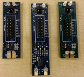
The second major component in the current sensor evaluation system are the daugh-tercards. Daughtercards are smaller boards that implement circuits specific to a current sensor product family and can connect to the motherboard to access the sig-nal generator or measurement system. These daughtercards form the cornerstone of the evaluation system because they allow the user to actually evaluate the current sensors. A picture of the daughtercard for the Si892x product family is shown in
Figure 4-1. This section discusses the concepts behind the design of daughtercards as a module within the current sensor evaluation system and briefly reviews the specifics of individual daughtercards.
Figure 4-1: Photo of the Si892x daughtercard
One of the central ideas of the current sensor evaluation system is the concept of modularity. Rather than creating a singular board that demonstrates all products, the system can be separated into the motherboard and daughtercard. Because the
motherboard is designed to connect to a generic daughtercard interface, new daugh-tercards created after the release of this system can also be used. This modularity reduces the amount of design work for future products, because evaluation boards have the motherboard interface to use as a design guideline.
The motherboard interface provides the necessary signals required by Silicon Labs current sensors. The daughtercards are able connect to power, the signal generator and the measurement system. This interface is flexible enough to support most re-quirements for current sensing, including high-side vs low-side sensing, different input waveforms, analog and digital outputs, and logic signals from a microcontroller. This wide range of capabilities ensures that this current sensor evaluation system will be able to support future products. The pin assignments are shown in Table 4.1.
Pin Description Pin Description
1 9 V 17 3.3 V
2 GND 18 General purpose input output 0
3 GND 19 PWM
4 GND 20 General purpose input output 1
5 3.3 V 21 ADC0 6 GND 22 ADC1 7 𝑉𝑠𝑒𝑛𝑠𝑒+ 23 GND 8 𝑉𝑠𝑒𝑛𝑠𝑒− 24 GND 9 GND 25 Serial line 0 10 GND 26 Reset line
11 High side current input 27 Serial line 1 12 High side current output 28 GND
13 GND 29 Serial line 2
14 GND 30 GND
15 Low side current input 31 Serial line 3 16 Low side current output 32 GND
Table 4.1: Motherboard-Daughtercard connector pin assignment
While the daughtercards are greatly enhanced by the motherboard, they are also functional without the motherboard, which affords the user greater control over the evaluation. The motherboard provides a simple input and output system for evaluat-ing the device. It is understandable that users may desire to test the product under conditions that closely replicates their end application.
Users can provide their own inputs and outputs through numerous external con-nectors located on the daughtercard. Nodes on a daughtercard can be accessed through test points, turrets and terminal blocks. Standard lab equipment such as wires, oscilloscope probes and alligator clips can all be used to attach to these con-nectors. Examples of these connectors can be seen in Figure 4-1. On the left hand side of the daughtercard, turrets provide access to the current signal path. The tur-rets and PCB traces are rated for significantly higher current than the motherboard, allowing the user to test currents that exceed the range of the motherboard. On the right hand side of the board are test points that allow the user to directly access the output of the device.
The daughtercards form an essential portion of the current sensor evaluation sys-tem by allowing users to evaluate the device and associated circuitry. The mother-board and daughtercard interface supports all of the current Silicon Labs products and will reduce the developmental efforts of future evaluation boards by providing a standard. The remainder of this chapter focuses on important aspects of each of the four implemented daughtercards.
4.1 Si8540-DC
The Si8540-DC is the daughtercard for Si8540 current sensor. This daughtercard uses several capabilities of the motherboard-daughtercard system to support the product evaluation. As described in subsection 2.2.2, the Si8540 is powered from the input current and required a common-mode input voltage above 5 V. This necessitates the use of high-side current sensing as low-side current sensing would ground one input and fail to provide sufficient voltage for operation of the device. By using the high-side sensing capability provided from the signal generator to the daughtercard, the Si8540-DC is able to demonstrate the capabilities of the Si8540.
The other motherboard feature that the Si8540-DC uses is the signal generator. As discussed earlier, the signal generator is designed to terminate into a load resistance of 60 Ω. The motherboard provides a series 59 Ω, and the daughtercard provides
an additional 1 Ω. The Si8540-DC therefore implements its sense resistor as a 1 Ω resistor. Once again, as explained in the signal generator section, this allows the evaluation system to use low currents and still provide full scale results by increasing the voltage developed across the sense resistor.
4.2 Si85xx-DC
The Si85xx-DC is unique among the daughtercards because the Si85xx is the only current sensor that uses inductive coupling rather than sense resistance as the mea-surement technique. The device directly integrates the current passing through it, therefore we can’t artificially increase the sensed current as we did in the Si8540-DC and other daughtercards with a larger sense resistor. Furthermore, the Si85xx is a high frequency sensor and measures signals above 50 kHz.
Due to the above listed reasons, the Si85xx-DC uses the motherboard buck load instead of the signal generator. The high-side current from the high-side switch is passed through the Si85xx. This signal is both sufficiently high frequency, at 192 kHz, and sufficiently large in amplitude to show Si85xx operation.
4.3 Si890x-DC
The Si890x-DC is unique because the Si890x is a general purpose isolated ADC. The inputs to the Si890x products are expected to be voltages within the input range of the device. Therefore it was necessary to develop sensing circuitry to appropri-ately implement the sense resistor topology and scale the voltage to the appropriate amplitude.
The sense resistor topology is simple to design given the constraints of the signal generator module. The daughtercard is expected to present an impedance of 1 Ω, therefore the sense resistor is set to be 1 Ω. This will allow for a maximum of 100 mVpp across the sense resistor. This voltage is scaled by 30 to fit inside the full-scale input voltage of 3.3 V. This gain was implemented using a differential op-amp amplifier [4].
Figure 4-2: Motherboard measurements system requesting ADC data from the Si8900 over UART.
Another uniqueness of the Si890x is that the output is provided digitally over serial communication. This is in contrast to the analog outputs of all of the other devices. The motherboard measurement system can still be used as it supports digital communication as an input. The motherboard is capable of communicating over UART, I2C or SPI. An example of the UART communication is shown inFigure 4-2. The top trace represents the motherboard’s request for data and the bottom trace represents the measured data from the Si8900.
The Si890x-DC supports a number of the Si890x advanced features, such as pro-grammable gain, multiple ADC channels, continuous sampling and multiple reference voltages. These all can be accessed through the digital communication interface. The physical daughtercard supports these features by providing access to multiple ADC channels and references. Users can then use the supplied PC software to test various configuration.
4.4 Si892x-DC
The Si892x-DC is another daughtercard that uses the sense resistor topology of the evaluation system. The same design principal of the load impedance used in the Si8540-DC and Si890x-DC is once again used here. The input is similar to other daughtercards, however the output is slightly different. The output is analog and fully differential. This is fine as the motherboard measurement system supports differential measurements. Both the positive and negative outputs are carried to the motherboard and then processed as usual.
4.5 Summary
The daughtercards provide an essential portion of the current sensor evaluation system by implementing the device under test and its associated circuitry. The motherboard-daughtercard interface is able to supply power, signal generation and output mea-surement and is flexible enough to support future products. The motherboard and daughtercard can be used together to make use of the extensive functionality provided by the motherboard or they can be used individually for further customizable investi-gation. Individual daughtercards have specific circuitry to augment their capabilities such as differential amplifiers or communication lines.
Chapter 5
PC Software Design
The third and final component in the current sensor evaluation system is the PC software. The software augments the capabilities of the motherboard by providing a convenient interface to monitor the measurement system. Furthermore, the software provides access to the advanced functionality present on several daughtercards. This chapter details several design considerations in the software and communication with the motherboard.
5.1 Communication Scheme
A communication scheme between the motherboard MCU and PC was developed to allow for efficient collection and transfer of measurement data. Both the measurement system and motherboard to PC communication occur on the same MCU. In order to guarantee the time accuracy of measurement samples, it is important to design a system that can reliably measure and communicate in real time.
To understand the implemented design, it is important to understand the con-straints of the system. The measurement system was implemented on the mother-board using a C8051F340 microcontroller. This MCU has built-in ADC and USB communication. The goal was to maximize the sampling rate of the MCU to the ADC limit of 200 kilosamples per second. This would allow for the best temporal resolution. The best choice was to implement a non real-time solution which batched
data points to minimize communication overhead. Samples were periodically taken over a 9 ms window and then transferred over USB. This approached allowed for maximal temporal resolution and a simple implementation in firmware and software. Other architectures were considered, such continuous data streaming or an inter-rupt based architecture for measurements. Non-batched continuous data streaming has the issue of communication overhead, and also presents challenges in the frame rate of the display. An interrupt based methodology potentially leads to time inaccu-racies due to higher priority interrupts preempting the ADC interrupt and disrupting the periodic sampling.
5.2 Software Architecture
The associated software for the evaluation platform was developed using the Model-View-Controller design pattern in mind. This design pattern separates the user inter-face from the model that interacts with the MCU in order to separate the logic and representation. The model controls the USB communication with the motherboard MCU. This was developed using Silicon Labs’ USBxpress [13]. The model was then able to communicate instructions regarding measurement and advanced functionality to the motherboard.
In order to facilitate communication between the software and motherboard, an instruction set was developed to describe common operations. The instruction set enabled remote access to most MCU functionality, most importantly the ADC, USB, and serial communication features.
5.3 User Interface
A simple user interface was developed to enable users to observe the evaluation mod-ule and access advanced functionality. The user interface accessed the motherboard through the software model as explained above. After acquiring samples from the motherboard, these were plotted in a display similar to an oscilloscope. An example
Figure 5-1: Screenshot of the current sensor software user interface.
of this user interface can be seen in Figure 5-1. The display clearly supports viewing the waveform, basic waveform measurements, plot interaction, and product selection. Measurements such as amplitude, mean and frequency are provided. The plot sup-ports basic features such as zooming and panning. Product selection allows access to product specific features such as ADC channel selection, variable gain, and serial communication parameters.
5.4 Summary
The PC software provides a simple user interface for display using a connected com-puter. This greatly enhances the portability of the system and also allows for access to advanced functionality. The software implements sampling as a batched group of measurements over a predefined time window. These measurements are received from the motherboard, displayed and analyzed. The software improves the evaluation system by providing a simple measurement and configuration interface.
Chapter 6
System Performance
We have constructed an evaluation platform to allow for safer and simpler current sensor evaluation. To this end, the platform has been designed to meet certain ob-jectives:
∙ Low voltage and current. A significant disadvantage of prior work was that default circuitry operated at hazardous voltages and currents. This creates a hazardous working environment for engineers using the device. To this end, the evaluation platform has been designed to use low voltages and currents deemed non-lethal [5].
∙ Minimal external components. We want to minimize non-essential external equipment, especially equipment that may not be standard in common labo-ratory environments. A drawback of prior work was the need for high current power sources and loads or pre-existing setups for signal generation. The eval-uation system was designed to require minimal additional equipment - solely a wall adapter and computer.
∙ Simplicity. We want to make the evaluation platform simple to use. To this end, we want to minimize setup time and provide easy access to advanced functionality.
6.1 Low Voltage and Current
We will consider the peak voltage and current used by existing and proposed works. The results of this are summarized in Table 6.1. The default configuration of the current sense motherboard has significantly lower peak voltage and peak current than all other previous evaluation boards. The evaluation system was designed to significantly reduce hazards associated with working with AC line voltages or high currents. The peak current was reduced to 100 mV into a 60 Ω terminating load. Human resistance is significantly higher and will result in a much lower current if the user somehow enters the conducting path. To this end, the constructed system is successful in improving safety by reducing the peak voltage to 9 V and peak current to 100 mV.
Platform Peak Voltage Peak Current
Si85xx-EVB - 5 A
Si890x-PWR-EVB 120 Vrms 10 A
Open-Loop-POL 15 V 10 A
Constructed System 9 V 100 mV
Table 6.1: Summary of voltage and current for evaluation systems.
6.2 Minimal External Components
We examine how the system compares with prior work in the number of required additional components. The results of this are summarized in Table 6.2. The con-structed system requires the least number of external components, simply a standard power source and a computer, both of which are standard lab equipment. The design is extremely portable and can be used outside of lab environments with an AC wall adapter and laptop. To this end, the system is successful by minimizing external components and enhancing portability.
Platform ExternalComponents Specialized Components Si85xx-EVB 4 high frequency high current source
Si890x-PWR-EVB 3 high power load,
non-standard connectors Open-Loop-POL 5 high power digital load
Constructed System 2
-Table 6.2: Summary of external components required for evaluation systems.
6.3 Simplicity
We consider how the constructed system performs with respect to prior work. To aid in this evaluation, we investigate setup time and accessibility of advanced features. A summary of these results is presented inTable 6.3. It can be seen that the constructed system requires less setup than existing solutions. In addition, the constructed sys-tem allows the user to access advanced features without additional effort. This is a significant improvement over existing systems. To this end, the system is successful by minimizing setup time and providing easy access to features, thereby improving simplicity.
Platform Required Setup
Si85xx-EVB solder header pin adapter, create high frequency, high current source along with reset logic signals
Si890x-PWR-EVB solder non-standard 3x3 output connector, attach board inline with AC mains device, compile flash code for ad-vanced functionality
Open-Loop-POL obtain five different pieces of external equipment, includ-ing high power digital load rated for 10 A
Constructed System plug adapter into wall, plug USB into computer Table 6.3: Summary of setup for existing and constructed evaluation systems.
Chapter 7
Conclusion
7.1 Summary
The goal of the work presented was to create a simpler and safer evaluation system for Silicon Labs’ current sensor products. We showed the need for such a product by analyzing existing work and proposed an motherboard, daughtercard, software evaluation system as a solution. The proposed work was laid out and constructed. Extensive validation has been done to demonstrate its functionality and improvement over existing systems. The key to success of the system lies within the modularity and functionality of the motherboard and daughtercard system for simplicity as well as the increased sense resistance for safety.
7.2 Future Work
7.2.1 High Frequency Measurements
A drawback of the implemented DC to DC buck converter is that the switching waveforms are too fast to be effectively sampled by the measurement system. The circuit could have been designed for a lower switching frequency with larger capacitors and inductors. Furthermore, the measurement system could be upgraded to a MCU with a faster sampling frequency. These two changes would allow for the measurement
system to evaluate the high frequency buck converter.
7.2.2 Future Daughtercards
Daughtercards were designed for all existing Silicon Labs current sensors, however several new products are poised to be launched over the next several years. Potential development could focus on development of new daughtercards for the current sensor motherboard. Furthermore, the corresponding software must be modified if advanced functionality support is desired for the new products.
Bibliography
[1] Analog Devices. A technical tutorial on digital signal synthesis. Technical report, 1999.
[2] John G. Kassakian. Principles of Power Electronics. Addison-Wesley, 1991, 1991.
[3] Linear Technology. Current Sense Basics. Technical report, 2005.
[4] R. Mancini. Op Amps for Everyone. Texas Instruments Design Reference, (August):279–280, 2002.
[5] Occupational Safety and Health Administration. Controlling Electrical Hazards. Technical report, Occupational Safety and Health Administration, 2002.
[6] Silicon Laboratories Inc. Si85xx Unidirectional AC CUrrent Sensors. Technical report, 2009.
[7] Silicon Laboratories Inc. Open-Loop POL Evaluation Board User’s Guide. Tech-nical report, Silicon Lanoratories Inc, 2010.
[8] Silicon Laboratories Inc. Si85xx Unidirectional AC Current Sensor Target User’s Guide. Technical report, 2010.
[9] Silicon Laboratories Inc. Using Si85xx Current Sensors in Switch-Mode Power Supplies. Technical report, 2010.
[10] Silicon Laboratories Inc. Isolated Monitoring ADC. Technical report, 2012. [11] Silicon Laboratories Inc. Si890x Digital Isolator-Based, 10-Bit Isolated
Monitor-ing ADC User’s Guide. Technical report, 2012.
[12] Silicon Laboratories Inc. High-Side Current Sense Amplifier. Technical report, Silicon Laboratories Inc, 2013.
[13] Silicon Laboratories Inc. USBxpress, 2013.
[14] Silicon Laboratories Inc. Isolated Amplifier for Current Shunt Measurement. Technical report, 2015.
[15] Texas Instuments. LM7321x Single and LM7322x Dual Rail-to-Rail Input and Output Âś 15-V , High-Output Current and Unlimited Capacitive Load Opera-tional Amplifier. Technical report, 2015.
[16] Silvio Ziegler, R.C. Woodward, H.H.-C. Iu, and L.J. Borle. Current Sensing Techniques: A Review. IEEE Sensors Journal, 9(4):354–376, 2009.