Charge Carrier Dynamics in Lead Sulfide Quantum Dot Solids
by
Rachel Hoffman Gilmore
Bachelor of Chemical Engineering Cornell University, 2011
Master of Science in Chemical Engineering Practice Massachusetts Institute of Technology, 2013
Submitted to the Department of Chemical Engineering in Partial Fulfillment for the Degree of
of the Requirements
Doctor of Philosophy in Chemical Engineering
at the
Massachusetts Institute of Technology
February 2018
l 3
0 2018 Massachusetts Institute of Technology. All rights reserved.
Signature of Author:
Signature
Department of Chemical Engineering August 29th 2017
redacted
Certified by:-,
Signature redacted
William A. Tisdale
Charles and Hilda Roddey Career Development Professor in Chemical Engineering Thesis Supervisor
ned hSignature
redacted
Patrick Doyle
Robert T. Haslam (1911) Professor of Chemical Engineering Chairman, Committee for Graduate Students
ARCHIVES
MASSACHUSETS INSTITUTE OF TECHNOLOGY
DEC 13 2017
Charge Carrier Dynamics in Lead Sulfide Quantum Dot Solids
by
Rachel Hoffman Gilmore
Submitted to the Department of Chemical Engineering on August 29th , 2017 in partial fulfillment of the requirements for the degree of Doctor of Philosophy in Chemical Engineering
Abstract
Quantum dots, also called semiconductor nanocrystals, are an interesting class of materials because their band gap is a function of the quantum dot size. Their optical properties are not determined solely by the atomic composition, but may be engineered. Advances in quantum dot synthesis have enabled control of the ensemble size dispersity and the creation of monodisperse quantum dot ensembles with size variations of less than one atomic layer. Quantum dots have been used in a variety of applications including solar cells, light-emitting diodes, photodetectors, and thermoelectrics. In many of these applications, understanding charge transport in quantum dot solids is crucial to optimizing efficient devices. We examine charge transport in monodisperse, coupled quantum dot solids using spectroscopic techniques explained by hopping transport models that provide a complementary picture to device measurements.
In our monodisperse quantum dot solids, the site-to-site energetic disorder that comes from size dispersity and the size-dependent band gap is very small and spatial disorder in the quantum dot superlattice often has a greater impact on charge transport. In Chapter 2, we show that improved structural order from self-assembly in monodisperse quantum dots reduces the interparticle spacing and has a greater impact than reduced energetic disorder on increasing charge carrier hopping rates. In Chapter 3, we present temperature-dependent transport measurements that demonstrate again that when energetic disorder is very low, structural changes will dominate the dynamics. We find increasing mobility with decreasing temperature that can be explained by a 1-2 A contraction in the edge-to-edge nearest neighbor quantum dot
spacing. In Chapter 4, we study optical states that are 100-200 meV lower in energy than the band gap. Because we work with monodisperse quantum dots, we are able to resolve this trap state separately from the band edge state and study its optical properties. We identify the trap state as dimers that form during synthesis and ligand exchange when two bare quantum dot surfaces fuse. The findings of this thesis point to the importance of minimizing the structural disorder of the coupled quantum dot solid in addition to the energetic disorder to optimize charge carrier transport.
Thesis Supervisor: William A. Tisdale
Acknowledgements
There are many people I would like to thank for their contributions this thesis and my time in graduate school at MIT. First, I would like to thank the National Science Foundation Graduate Research Fellowship Program and the Department of Energy for funding my graduate studies. I would also like to acknowledge the Center for Functional Nanomaterials at
Brookhaven National Laboratory where I collected a large fraction of the experimental data presented in this thesis.
I would not have come to graduate school without the support and encouragement of my professors at Cornell University, particularly Professors T. Michael Duncan, Susan Daniel, and Tobias Hanrath. I would also like to thank the graduate student I worked with during my undergraduate research, Joshua Choi, and the rest of the Hanrath Lab for making undergraduate research such a great experience that I wanted to continue in graduate school.
I am extremely grateful to my thesis advisor, Will. I have been privileged to be part of founding this welcoming, fun-loving, and supportive group while doing great science, and I cannot thank Will enough for creating this atmosphere. Will has been a source of boundless enthusiasm and optimism and it has been a real pleasure to be able to work with him.
I would like thank my thesis committee members, Moungi Bawendi and Bill Green for their advice and input throughout my PhD. It has been extremely helpful to have the perspective of Moungi's decades of experience in the quantum dot field, and I am consistently impressed by Bill's insightful questions.
I would like to thank my many collaborators. First, endless thanks for Matt Sfeir at the Center for Functional Nanomaterials at Brookhaven National Lab. A majority of the
experimental work in this thesis was conducted in his optics lab, and this would not have been possible without his time and dedication and willingness to help me set up any and all
experiments I needed. I would like to thank Adam Willard for his advice and input on theoretical simulations and model to explain my spectroscopy data and for granting me access to his
computer cluster to run kinetic Monte Carlo simulations. I would also like to thank Yun Liu, Huashan Li, and Jeff Grossman for collaborating on atomistic calculations of the energy
structure of QD dimers. I am grateful to Detlef Smilgies at the Cornell High Energy Synchrotron Source and Kevin Yager at the National Synchrotron Light Source II at Brookhaven National Lab for collecting GISAXS measurements to complement my transport measurements, sometimes at very short notice.
I would like to extend a big thank you to the members of the Tisdale Lab. In particular, thank you to Liza Lee for collaborating with me on kinetic Monte Carlo and Pauli maser equation simulations to fit my experimental work. I am thankful for her endless patience in explaining the theory and simulation techniques to me and I learned so much from her in this
process. This thesis would not have been possible without the excellent work done by Mark Weidman, developing the PbS QD synthesis and making all the QDs I used in my thesis, as well as conducting extensive studies of superlattice formation and ordering that informed the
interpretation of my transport measurements. Thanks to Matt Ashner for being my laser lab buddy, building the transient absorption setup in our lab, and helping collect data on my PbS QDs. I greatly appreciate the many hours Nabeel Dahod spent searching for the needle in a haystack that is HR-TEM of QD dimers as well as his other TEM and synthetic work to support my thesis. I would also like to thank Wenbi Wu for helping to collect and analyze data this summer as I worked to wrap up my thesis and I am excited for her to build on some of my work in her thesis. I am grateful to Sam Winslow for analyzing GISAXS data this summer to
complement my temperature-dependent transport measurements on a very short timeline this summer. I would like extend my thanks to all the other members of the Tisdale Lab for creating such a great working environment - Ferry, Jolene, Aaron, Lisa, Pooja, Yunan, Dan, Oat, SK, Kris, Katie, Robert, Michael, Leo, Deepankur, and Barb.
I want to thank the friends with whom I went through the ups and downs of the ChemE first year classes and Practice School - Lea, Rosanna, Renee, Aanchal, Adam, Kendele, Katie, Ray, Ben, Sakul, Mariah, Anashuya, Yuqing, and Lucas. I am also grateful for the friends from the Bulovic lab that I met in the solid state physics course I took second semester - Joel, Farnaz and Wendi - as well as those in the Bawendi lab - Justin, Michel, Lea, and Igor. I would also like to thank Libby Mahaffy, Jean Belbin, Suzanne Maguire, Joel Dashnaw, Sydney Greenley-Kois, Sharece Corner, Eileen Demarkles, and Suzanne Ronkin for their encouragement and support during my graduate studies.
The MIT Science Policy Initiative has been an important part of my graduate experience over the past three years. I thank Bill Bonvillian and Kate Stoll at the MIT Washington Office for all their time and effort to support our many programs. I am very grateful to the many
members of the MIT administration who financially support SPI and encourage us as we develop our programming including Deans Waitz, Sipser, Ortiz, and Staton, and VP of Research Zuber. I also want to express my thanks to the other members of the SPI Exec boards with whom I had the opportunity and pleasure of working as well as the many friends I have made through SPI
-Lisa, Abigail, Shelby, Jack, Peter, Angela, Lilia, Georgia, Kenny, Jen, Eli, Max, Daniel, Alec, Sarah, Hannah, Scott, Daniel and many others. I cannot wait to see what the new leadership has in store for the upcoming year.
I also thank my high school friends, Izzy and Jennie, and college friends, Andrea and Dayna, for their encouragement, advice, and friendship throughout graduate school.
I am grateful to my Mom and Dad for their support and encouragement to pursue this path and keep persisting even when I had doubts, and to my sister and brother, Abby and Henry, for being there for me and believing in me.
Finally, I would like to thank my wonderful husband and best friend, Daniel, for his support, encouragement, and unshakeable faith in my ability to achieve anything I set my mind to. I appreciate all the times he has cooked me dinner and cleaned the apartment so I could work to complete this thesis. He has kept me grounded and motivated, and for him I am forever grateful.
Table of Contents
A bstract ... 3
A cknow ledgem ents... 5
Table of Contents... 9
List of Figures ... 1
List of Tables ... 19
Chapter 1 Introduction ... 21
1.1 N anocrystal Quantum Dots... 21
1.2 Lead Sulfide Quantum Dot Synthesis... 22
1.3 Quantum Dot Electronic Structure... 23
1.4 Q D Solids: Self-assem bly and Ligand Exchange ... 25
1.5 Transport in Quantum Dot Solids... 26
1.5.1 Excitons versus free carriers ... 26
1.5.2 Charge carrier hopping m echanism s ... 26
1.5.3 Temperature dependence of charge carrier hopping ... 27
1.5.4 Experim ental transport m easurem ent techniques... 28
1.5.5 Charge carrier delocalization and band-like transport ... 29
1.5.6 Trap states ... 30
1.6 Transient Absorption Spectroscopy ... 31
1.7 Thesis Overview ... 36
Chapter 2 Charge Carrier Hopping Dynamics in PbS Quantum Dot Solids of Varying Size and Size D ispersity... 37
2.1 Introduction... 37
2.2 Fabricate Samples of Varying Size and Size Dispersity... 38
2.3 Transient Absorption of Coupled QD Solids... 40
2.4 Kinetic M onte Carlo M odel to Fit Dynam ics ... 41
2.5 Single Q D Linew idth ... 44
2.6 Im pact of Size Dispersity on Transport ... 49
2.8 C onclusions... 54
2.9 Experimental Methods... 55
2.10 Appendix A: Fitting Absorption Spectra to Determine Peak and Linewidth.... 57
2.11 Appendix B: Experimental Data for All QD Sizes... 58
2.12 Appendix C: Comments on Energetic Alignment in the KMC model... 60
2.13 Appendix D: Discussion of Assumptions about the Superlattice Structure ... 63
Chapter 3 Temperature-Dependent Charge Transport ... 67
3.1 Introduction ... 67
3.2 Temperature-Dependent Transient Absorption ... 67
3.3 Pauli Master Equation Approach to Data Fitting... 70
3.4 Temperature-Dependent Hopping Rates Based on Previous Model ... 71
3.5 Global Fitting Model Predicts Superlattice Contraction... 74
3.6 GISAXS Reveals Superlattice Distortion with Decreasing Temperature... 76
3.7 Increasing Mobility with Decreasing Temperature ... 78
3.8 C onclusions... 80
3.9 Experimental Methods ... 80
3.10 Appendix A: Effect of QD shape on minimum center-to-edge distance... 82
3.11 Appendix B: Lattice Distortion from GISAXS ... 83
Chapter 4 Origin of Trap States ... 85
4.1 Introduction ... 85
4.2 Photoluminescence from Band Edge and Trap States ... 86
4.3 Transient Absorption Directly Excites Trap States and Monitors De-trapping. 87 4.4 Trap State Dynamics are Similar to that of Large QDs ... 90
4.5 Trap States are QD Dimers ... 91
4.6 Expected Electronic Structure of a QD Dimer ... 95
4.7 Comparison to Trap State Literature... 97
4.8 C onclusions... 100
4.9 Experimental Methods ... 100
C hapter 5 O utlook ... 103
List of Figures
Figure 1.1. The ruby red and yellow colors in stained glass windows, such as those in the iconic north rose window of Notre-Dame de Paris pictured here, are a result of gold and silver
nanoparticles in the glass ... 21 Figure 1.2. Schematic showing the size-dependent band structure. ... 24 Figure 1.3. Absorption spectrum of PbS QDs in tetrachloroethylene. ... 25
Figure 1.4. Normalized photoluminescence intensity as a function of temperature. PL is low near room temperature when excitons rapidly dissociate, and high at low temperatures when charge carriers rem ain as excitons... 26 Figure 1.5. Schematic of a transient absorption experiment... 32 Figure 1.6. (a-c) Schematics of possible TA signals. (d) Sample TA spectrum of 5.8 nm PbS QDs in tetrachloroethylene showing typical features for a QD with an exciton in the band edge state. ... 3 2 Figure 1.7. Transient absorption signatures of hot electron relaxation in 5.8 nm QDs in
tetrachloroethylene. (a) 2D colorplot showing spectral changes as a function of time. (b) TA spectra at selected tim e delays ... 33 Figure 1.8. Photoluminescence and transient absorption lifetimes from PbS QDs in
tetrachloroethylene... 34 Figure 1.9. Transient absorption signatures of Auger recombination and calculation of the
absorption cross section. (a) Increasing the pump fluence increases the number of absorbed photons per QD. Excitons on QDs with more than I exciton undergo Auger recombination, reducing the TA bleach signal in a few hundred picoseconds. (b-c) The absorption cross section can be estimated from a plot of the bleach intensity at I ns, after Auger recombination is
complete but before appreciable single exciton recombination, versus the excitation fluence. This is shown for 5.8 nm QDs in (b) and 4.9 nm QDs in (c)... 35 Figure 2.1. Tuning size dispersity in PbS quantum dot solids. (a) Solution phase absorption (solid lines) and emission (dashed lines) spectra for the ten PbS quantum dot batches used in this study. (b) Ensemble absorption linewidth (standard deviation) as a function of first absorption peak energy, with small QDs with 6 < 5% in blue, large QDs with 6 < 4% in orange and large QDs with 6 ~ 3.3% in red. The dashed lines show the calculated size dispersity of the ensemble assuming a delta function homogeneous linewidth. (c) HR-SEM image of a PbS QD solid (-100 nm thick, 0.92 eV absorption peak, d = 5.8 nm, 6 < 4.1%) at ambient temperature following ethanethiol ligand exchange. (d) Grazing incidence small angle X-ray scattering (GISAXS) pattern of a similar film (1.17 eV absorption peak, d = 4.9 nm, 6 < 3.5%), showing some
Figure 2.2. Absorption spectra of quantum dot solids with ethanethiol ligands. The colors are consistent w ith those in Figure 2.1 a... 39 Figure 2.3. Transient absorption tracks the average energy of QDs containing excited charge carriers. (a, b) TA data collected from ethanethiol treated solids made from PbS QDs with 6 <
5.4% (a) and 6 < 3.5% (b). Solid white lines are the ground state linear absorption spectra.
Dashed lines show the TA bleach peak position as a function of time. (c, d) Spectral slices at selected times showing the redshift of bleach peak in the 6 < 5.4% sample (c) but not in the 6 <
3.5% sample (d). Dots represent data and lines show Gaussian fits to the peaks. (e, f) Bleach
peak energy as a function of time for the 6 < 5.4% (e) and 6 < 3.5% (f) samples... 41
Figure 2.4. Kinetic Monte Carlo fits to transient absorption data. (a) KMC fit for a representative solid of small quantum dots with 6 < 5% (same sample as shown in Figure 2.3a). (b) KMC fit for a representative QD solid with 6 < 3.3% (same sample as shown in Figure 2.3b). (c) KMC fit for a representative QD solid with 6 ~ 4%. Colored points are the data (same colors as Figure 2.1 a), and black lines are the KMC fits with the gray shaded area showing one standard deviation error in the fitting param eters. ... 44 Figure 2.5. Fundamental parameters extracted from KMC fitting. (a) Inhomogeneous linewidths (standard deviation) of the ten PbS QD samples as found from the fitted energy redshift in the KMC simulations. (b) Homogeneous linewidth (standard deviation) for the absorption (circles) and emission (points) spectra, calculated from the ensemble linewidth and the fitted
inhomogeneous linewidth. The solid (absorption) and dashed (emission) lines show the 1/?R2 scaling expected for homogeneous broadening dominated by deformation-potential coupling to acoustic phonons.128 (c) Characteristic hopping time, defined as the inverse hopping rate pre-factor adjusted for the number of nearest neighbors in the lattice. Symbol colors are consistent w ith F igure 2.1 b... 46
Figure 2.6. Kinetic Monte Carlo fits for the small samples with size dispersity 6 < 5% with two time constants representing different hopping rates for electrons and holes... 48 Figure 2.7. Grazing-incidence small-angle (left) and wide-angle (right) X-ray scattering
(GISAXS and GIWAXS) patterns for quantum dot solids with 6 < 3.5% (top) and 6 < 4.9%
(bottom) with native oleic acid ligands. The 6 < 3.5% solid shows a highly ordered superlattice with individual QDs all oriented in the same way with the atomic planes aligned. In contrast, the 6 < 4.9% sample shows much less order, both for the superlattice and the individual QD
orientation. The poorer self-assembly in the 6 <4.9% solid results in an average edge-to-edge QD spacing of 3.1 nm, which is 0.8 nm larger than that of the 6 < 3.5% sample (a 35% increase).
... 5 0
Figure 2.8. Intrinsic charge carrier hopping rates as a function of center-to-center QD spacing (a) Hopping times from Figure 2.5 plotted vs center-to-center QD spacing, rather than QD diameter. (b) The hopping rate decreases with increasing center-to-center spacing. Dashed line shows an
exponential fit. (c) Even after accounting for a greater distance travelled per hop, mobility and diffusivity decrease with increasing center-to-center QD spacing. Dashed line shows dc 49 fit. 51
Figure 2.9. (a) The percentage of the hopping time that is attributed to energetic disorder, as given by (1/ktOt-1/8k')/(l/ktot). (b) Calculated intrinsic charge carrier mobility and diffusivity as a function of Q D size... 52 Figure 2.10. Schematic showing a homogeneously broadened QD solid with an inhomoeneous linewidth much less than both the single QD (homogeneous) linewidth and the available thermal energy at room tem perature. ... 52 Figure 2.11. (a) Mean squared displacement as a function of time from the KMC simulation. The dashed line shows an example of a linear fit at long times to get the diffusivity from the KMC simulation. (b) Simulated charge carrier diffusion length as a function of carrier lifetime... 53 Figure 2.12. Fitting absorption spectra to determine peak energy and linewidth. (a) Sample fit (black solid line) to absorption spectrum (purple) with E4 Rayleigh scattering and three Gaussian peaks for the defined features (dotted lines, band edge peak in gray). (b) Sample absorption spectra fits for monodisperse (top) and polydisperse (bottom) samples near the first absorption peak, showing the fitted peak position in dark gray. (c) Comparison of the absorption linewidth for the fit (open circles) to that determined by measuring the half-width at half-maximum (HWHM, triangles) on the low energy side of the peak. (d) Comparison of the calculated
homogeneous linewidth for the absorption spectra fits (open circles), absorption spectra HWHM (triangles), and PL (closed circles). ... 57
Figure 2.13. (a-j) GISAXS data for all samples, labelled with the center-to-center spacing, dc, QD diameter, d, and size dispersity, 6. Because QDs are actually faceted, not spherical, very close packing with aligned crystal facets can result in d,, < d.136 (k) Azimuthally integrated
GISAXS intensity. (1) Center-to-center spacing, with dashed line showing expected spacing based on sizing curve and 0.5 nm edge-to-edge spacing for ethanethiol... ... .. . . 58
Figure 2.14. (a-j) Transient absorption data for all samples with peak bleach (dashed) and linear absorption spectrum (solid line). Border colors are the same as the spectra in (k). ... 59
Figure 2.15. (a-j) Kinetic Monte Carlo fits (solid lines) for all samples assuming symmetric conduction and valence bands, with error bounds (shaded gray) and data points shown in same colors as in the solution absorption (solid) and photoluminescence (dashed) spectra in (k)... 61 Figure 2.16. (a-j) Kinetic Monte Carlo fits (solid lines) assuming all energetic variation is in one band (could be either conduction band or valence band) for all samples, with error bounds (shaded gray) and data points shown in same colors as in the solution absorption (solid) and photolum inescence (dashed) spectra in (k)... 62 Figure 2.17. The equivalent of Figure 2.5 for fundamental parameters extracted from KMC simulations assuming all energetic variation in one band (conduction or valence band). (a) Inhomogeneous linewidths (standard deviation) of the ten PbS QD samples as found from the
fitted energy redshift in the KMC simulations. (b) Homogeneous linewidth (standard deviation) for the absorption (circles) and emission (points) spectra, calculated from the ensemble linewidth and the fitted inhomogeneous linewidth. The solid (absorption) and dashed (emission) lines show the 1/R2 scaling expected for homogeneous broadening dominated by deformation-potential coupling to acoustic phonons. (c) Characteristic hopping time, defined as the inverse hopping rate pre-factor adjusted for the number of nearest neighbors in the lattice. ... 63 Figure 2.18. (a) KMC simulation with a BCC lattice considering hopping to the 8 nearest
neighbors only (black), and with a distance-dependent hopping rate, allowing hopping as far as 10 times the nearest neighbor distance (green). (b) Comparison of KMC simulation with BCC (black) and FCC (blue) lattices. Dashed lines give the standard deviation of 10 simulations. (c) Comparison of KMC simulation with BCC (black) and disordered (red) lattices. A tunneling constant of f = I A is used to calculate the tunneling rate as a function of edge-to-edge spacing for the disordered lattice.64 Dashed lines give the standard deviation of 10 simulations. (inset) Zoom in on the fit in the first 140 ps. (d) Distribution of center-to-center spacing for the BCC lattice and the disordered lattice that is derived from a BCC lattice. ... 65 Figure 3.1. Transient absorption peak bleach redshifts for as a function of sample temperatures. (a) Linear absorbance spectra of the three QD ensembles used in this study. (b) Transient absorption color plot for 4.2 nm QDs at 300 K (c) Bleach peak energy as a function of time for several temperatures (labeled on graph) for the 5.0 nm QDs. (d) The data in panel (c) plotted as a change in peak energy relative to the energy at zero delay time. The colors used for each
tem perature are consistent w ith panel (c). ... 68 Figure 3.2. Transient absorption peak bleach redshifts for 4.2 nm (a) and 5.8 nm (b) QDs as a function of temperature. The data in panel (b) is plotted as a change in peak energy relative to the energy at zero delay time in (c). The colors used for each temperature are consistent across the p an els. ... 69 Figure 3.3. Linear absorption spectra as a function of temperature for 4.2 nm and 4.9 nm QDs. 69 Figure 3.4. Fits based on model from Chapter 2. (a) Normalized photoluminescence intensity is used to estimate the fraction of dissociated excitons as a function of temperature. (b-d) Model fit to data at each temperature for the 4.2 nm (b) 5.0 nm (c), and 5.8 nm (d) QD solids. The colors used for each temperature are consistent throughout the figure. (e-f) Fitted hopping rates as a function of temperature for the 5.0 nm QD solids ... 73 Figure 3.5. Fits with the global hopping model for the 4.2nm (a), 5.0 nm (b), and 5.8 nm (c) QD solids. (d) Predicted change in edge to edge spacing based on the model. (e-j) Fitted hopping rate prefactors (open symbols) and per QD pair total hopping rates (closed symbols) for the 4.2 nm (e-f), 5.0 nm (g-h), and 5.8 nm (i-j) QD s... 75
Figure 3.7. Temperature-dependent lattice distortion of an ordered superlattice of 5.7 nm QDs with oleic acid ligands. (a) GISAXS patterns at 298 K showing a face-centered cubic lattice and (b) 133 K showing a body-centered tetragonal lattice. (c) Change in neighbor center-to-center spacings with temperature for a and b axes (black, open circles), c axis (blue, open squares), di1o
direction (red, open triangles), and nearest neighbors (purple crosses). (d, e) Schematics showing the superlattice distortion as a function of temperature with FCC unit cell (blue) and BCT unit cell (red )... 7 7 Figure 3.8. Temperature-dependent lattice distortion of an ordered superlattice of 5.0 nm QDs with ethanethiol ligands. (a) GISAXS patterns at 298 K with expected FCC diffraction peak positions and (b) 160 K with expected BCT peak positions based on the lattice distortion model described in the text. (c) Change in neighbor center-to-center spacings with temperature
for a and b axes (black, open circles), c axis (blue, open squares), duo direction (red, open
triangles), and nearest neighbors (purple crosses) ... 78 Figure 3.9. Calculated mobility from KMC simulations based on the global hopping model fit for the fast (a) and slow (b) hopping rates... 78
Figure 4.1. Emission from band edge and trap states in ethanethiol-treated PbS QD solids. (a) Photo luminescence spectra as a function of temperature showing PL from the band edge state at room temperature and from the trap state at lower temperatures. (b) Schematic showing much higher density of states at the band edge than at the trap state energy, so that at room
temperature, charge carriers are thermalized into the band edge states. (c) Ratio of band edge to trap state PL as a function of temperature (filled circles). A fit (dashed line) gives the energetic barrier between QDs and the density of trap states... 86 Figure 4.2. Excite trap states in PbS QD solids and observe de-trapping in coupled films. (a)
Schematic showing population of the trap state followed by upconversion to the band edge state. (b-f) Color plots showing excitation of the mid-gap trap state QD solids (d= 4.2 nm, 6= 2.1-3.0%) with varying ligand lengths. The pump spectra and QD solution absorption spectra are shown overlaid for reference. (g) Spectra at early and late times for the ethanethiol treated solid (b), with peak position and fwhm for the trap state and band edge peaks. (h) Integrated peak intensities as a function of delay time for the ethanethiol treated solid (b). (i-j) Color plots
showing dynamics following mixed excitation of the trap and band edge state. (k-l) Excitation of the mid-gap state and band edge state in larger, monodisperse QD solids (d= 4.9 nm, 6 = 0.6-0 .8% )... 87 Figure 4.3. Transient absorption exciting at the band edge peak for QD solids with thiol ligands of varying lengths. A transient redshift indicating charge transport in the observed time window is present for ethanethiol and butanethiol QD solids, but not for octanethiol, dodecanethiol, or o leic acid ... 88 Figure 4.4. Transient absorption spectroscopy showing excitation of the trap state and
repeated from Figure 4.2. (middle row) Spectra at I ps and 400 ps for the QD solids in the row above. (bottom row) Population dynamics of the band edge and trap states for the QD solids show n in the top row ... 89 Figure 4.5. PbS QDs with mercaptopropionic acid (top row) and tetrabutylamonium iodide (bottom row) ligands also show trap state excitation and upconversion to the band edge state... 89 Figure 4.6. Trap state bleach dynamics. (a) Trap state bleach intensity in QD solid with oleic acid ligands as a function of delay time and excitation power showing dynamics characteristic of Auger recombination. (b) Decay time constant as a function of number of excitons absorbed per
QD for the trap state and various sizes of QD band edge states. (c) Bleach intensity at Ins as a function of excitation fluence with experimental data shown with open circles and a fit to the data to determine the absorption cross section shown with a dashed line. (d) Trap state and band edge bleach dynamics in ethanethiol-treated QD solid excited at the trap state energy with varying excitation powers at 300 K. Fitted time constants are 39 5 ps (0.8x 10¹⁵ photons/cm2
),
35 3 ps (1.6x10'5 photons/cm2), 34 2 ps (3.6x10¹⁵ photons/cm2), and 520 + 40 ps (all). The
contribution from the fast component increases with increasing fluence. (e) Dynamics at 80 K. (f) Schematic showing proposed de-trapping mechanism... 90 Figure 4.7. (a) TEM micrograph of monodisperse 4.9 nm QDs with oleic acid ligands showing an absence of large QDs, but the presence of a QD dimer. (b) HR-TEM micrograph of a dimer with FFT of the entire dimer and the left and right QD within the dimer, all identical and
showing (100) planes oriented to the surface, indicating attachment on the (100) facet. (c) HR-TEM micrograph of a dimer with a twinning boundary at the attachment interface. FFT shows the left side of the dimer has (100) planes oriented to the surface while the right side has (111) planes, but the radially aligned peaks indicate aligned lattice planes across the dimer confirming
fused attachm ent. ... 92 Figure 4.8. FFT analysis of HR-TEM images. (a) FFT analysis of a monolayer of unattached, randomly oriented QDs shows many FFT spots at different azimuthal positions. (b) FFT analysis for the dimer shown in Figure 4.7 shows two different lattice planes aligned and epitaxially attach ed . ... 9 3 Figure 4.9. Trap state excitation of oleic acid-capped QDs in solution, oleic acid-capped QD solids, and following ligand exchange for ethanethiol. The optical density at the band edge peak absorption was 0.2 for the solution sample, 0.1 for the oleic acid sample, and 0.08 for the EMT sample. Thus, the concentration of trap states seems to be the same in solution and in a QD solid with oleic acid ligands, but is higher for ethanethiol-treated solids, even after accounting for an increase in absorption cross section for the shorter ligands. ... ... . . . 94 Figure 4.10. Trap state excitation in QDs synthesized with PbO (a-b) or PbAc2 (c). (b) has a
longer w avelength pum p pulse than (a)... 94 Figure 4.11. Calculated trap state depth for different QD shapes (truncated octahedron,
tight binding approximations. 120,162 Calculations with a confining potential barrier of 1.0 eV162
are shown with solid lines and of 1.6 eV93 with dashed lines. Trap state depth extracted from transient absorption measurements are shown in red circles... 95 Figure 4.12. Sideview of the 2 nm diameter PbS QD. The black and yellow atoms represent Pb and S respectively. The colored boxes represent increasing degree of fusing in the QD dimers, from 4 to 12, 16, and 24 atoms. The fusing occurs along the (100) facet. The absorption spectra and (c) band edge states of fused dimers, compared with single isolated QD. (d) The
wavefunction of the conduction band minimum of a single dot, and that of the fused dimer with 12 atoms in the fused plane. Significant localization of the states along the fused region
compared to the delocalized states in the QD core for the single dot... 96 Figure 4.13. Sideview of the 2.5 nm diameter PbS QD. The black and yellow atoms represent Pb and S respectively. The colored boxes represent increasing degree of fusing in the QD dimers, from 4 to 12, 16, 24, and 32 atoms. The fusing occurs along the (100) facet. The absorption spectra and (c) band edge states of fused dimers, compared with single isolated QD. ... 97 Figure 4.14. Temperature-dependent photoluminescence spectra for (a) ethanethiol-treated and (b) benzoquinone and ethanethiol-treated PbS QD solids. Normalized spectra are shown in (b) and (e) respectively. Integrated PL intensity as a function of temperature are shown in (c) and (f).
... 9 8 Figure 4.15. Optically exciting the trap states in QD solids with and without benzoquinone
treatm ent. ... 99 Figure 4.16. Exciting QD solids with and without benzoquinone treatment at the band edge state. ... 9 9
List of Tables
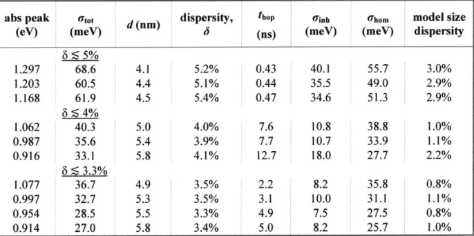
Table 2.1. Key parameters from experiment and simulations: fitted absorption peak maximum; fitted total absorption linewidth (standard deviation, utot); calculated QD diameter based on our sizing curve (d);20 calculated size dispersity assuming delta-function homogeneous linewidth, expressed as standard deviation of the mean diameter (6); the fitted hopping time constant, which is the reciprocal of the hopping rate prefactor, thop = 1/k'; fitted inhomogeneous linewidth from
TA experiments (Uinh); inferred homogeneous linewidth (Uhom from eq (2.4) using Utot from
column 2 and Oinh from column 6); and the "actual" size dispersity calculated from the fitted
Chapter 1
Introduction
1.1 Nanocrystal Quantum Dots
The unique optical properties of nanostructured materials have been employed for centuries, since long before their science was understood. For example, the vivid reds and yellows in stained glass windows found in European cathedrals from the 6th to 15th centuries are the result of gold and silver nanoparticles, respectively, that formed when gold chloride or silver nitrate was added during the glass-making process (Figure 1.1).'
Figure 1.1. The ruby red and yellow colors in stained glass windows, such as those in the iconic north rose window of Notre-Dame de Paris pictured here, are a result of gold and silver
nanoparticles in the glass.
The modem era of scientific research into semiconductor quantum dots (QDs), which are also called nanocrystals (NCs), began in 1981 when Alexei Ekimov of the USSR formed and studied the optical properties of semiconductor nanocrystals in a glass matrix.2 3 A few years later, Louis Brus of Bell Labs synthesized and studied the first colloidal semiconductor QDs.4-6 In 1993, Moungi Bawendi's new lab at MIT developed the first controlled, scalable synthesis for colloidal QDs, which they demonstrated with nearly monodisperse CdSe QDs.7
QDs are clusters of 1000-10,000 atoms that are -2-20 nanometers in diameter and exhibit optical properties that have both bulk and atomic character. A defining feature of
semiconductor QDs is a size-dependent band gap, which determines what colors of light the QDs will absorb or emit. Synthetic methods have now been developed for a variety of semiconductor QDs, including Cd, Zn, Hg, and Pb chalcogenides (S, Se, Te), InP, InAs, and perovskites.8-10 It is possible to engineer the shape of QDs"'-14 as well as make a variety of core-shell structures,15-17 which show near-unity quantum yields. Their optical properties span the near ultra-violet to the mid-wavelength infrared, making different types of QDs attractive materials for a wide variety of applications18 including display technologies,19 light-emitting diodes,20 solar cells,2 1
sensors.26 Lead sulfide (PbS) quantum dots are particularly promising for infrared applications because they are air stable and have a band gap that can be tuned across the near infrared (NIR) into the short-wave infrared (SWIR) from ~700nm to 2400nm (1.8eV to 0.5eV).2 7 28 PbS QD
photodetectors have figures of merit that outperform commercial technologies.29 They have been
used in IR LEDs,0 and are the absorber in QD solar cells with efficiencies exceeding 11%.21
Thus, QDs are a promising designer semiconductor for next-generation optoelectronic devices, in which one can imagine precisely tuning the semiconductor properties to match the desired application. They are very good at absorbing and efficiently emitting narrow spectrum
light, so their first commercial applications have been as color filters in display technologies such as televisions and monitors.19 However, other applications, such as solar cells or LEDs, require better control of the charge carrier transport, and how changing QD properties impacts transport in QD solids.
1.2 Lead Sulfide Quantum Dot Synthesis
Initial colloidal synthesis for PbS QDs was published by Hines and Scholes in 2003,9 a decade after CdSe QD synthesis was first reported. The synthesis was patterned on previous QD
synthesis methods for cadmium chalcogenides7 and PbSe,3
1 using lead oxide in oleic acid (OA)
to make lead oleate, and injecting bis(trimethylsilyl)sulfide (TMS) in octadecene (ODE) at elevated temperatures of 80-140'C. Varying the OA:Pb:S ratios and the injection temperature adjusts the kinetics of the nucleation and growth rates to control the QD size. This synthesis has
since been adapted to use either lead oleate or lead acetate,3 2 and is widely used in a variety of
devices.
Another hot-injection synthesis method developed by Cademartiri et al., and improved by Moreels et al.36 and Weidman et al.7 uses lead chloride and elemental sulfur precursors in oleylamine, which acts as both the stabilizing ligand and the solvent. This synthesis follows a diffusion-limited growth mechanism, and creates highly monodisperse PbS QDs that are lead-rich with both chlorine ions (from PbCl2) and oleylamine ligands on the surface. Size dispersity,
or the variation in QD sizes within an ensemble, determines the total linewidth of the ensemble absorption and emission spectra (inhomogeneous broadening is convolved with homogeneous
broadening to give the total linewidth) and the energetic disorder in a QD solid. It is thus a key parameter to optimize in synthesis, with monodisperse QDs (all QDs the same size), rather than polydisperse QDs (a range of QD sizes present), desired for most applications. The oleylamine
ligands are weakly bound to the QD surface, and rapidly detach and reattach, in equilibrium with free oleylamine in solution.36 Following synthesis, the oleylamine ligands are replaced with more
strongly bound oleate ligands at a density of about 3 per nm2 to ensure long-term colloidal
stability.36 The surface chlorine ions are believed to stabilize the QDs, making them air-stable for at least several months.27 The oleate and chloride ions also ensure charge neutrality of the
lead-rich QDs.36 While this synthesis is very successful for making QDs with band gaps lower in energy than 1.2 eV (1000 nm), it does not make the smallest QDs that are often used in
photovoltaics. Zhang et al.37 have adapted this synthesis to use TMS in place of elemental sulfur to extend the size range to these smaller QDs.
Additional synthetic methods to make monodisperse PbS QDs have been developed in recent years. Hendricks et al.38 developed a library of substituted thiourea precursors to precisely tune the nucleation rate kinetics with lead oleate and prepare monodisperse PbS QDs across a range of sizes at nearly full reaction conversion. Taking advantage of the excellent synthetic methods available for CdS and CdSe QDs, Beard and co-workers39 use a cation exchange
process to convert highly monodisperse CdS or CdSe QDs to PbS or PbSe QDs. PbC2 is used for the cation exchange, so these QDs have the chloride passivation that improves air stability. Larger PbS QDs can be made through the sequential addition of smaller QDs, which dissolve to create additional monomers in solution and grow the size of the original QDs through an
Ostwald ripening process.40
1.3 Quantum Dot Electronic Structure
The size-dependent band gap in semiconductor QDs arises when the size of the QD approaches and becomes smaller than the characteristic length scale of a charge carrier in the material. The charge carrier can be an electron, hole, or electron-hole pair, which is known as an exciton. The characteristic length scale is given by the Bohr radius:
aB =E - ao
m
where c is the dielectric constant of the material, m is the rest mass of an electron, m * is the effective mass of the charge carrier (electron, hole, or exciton), and ao is the Bohr radius of the hydrogen atom. The Bohr radius for the exciton in PbS is ~18 nm, so strong quantum
confinement is expected for typical quantum dot sizes (2-12 nm).4' Additionally, the effective
masses of the electron and hole in PbS are small and approximately equal (me* = 0.12m, mh* -0. 1i m), so both the electron and hole of dissociated excitons are strongly quantum confined.
To a first approximation, the band gap of a QD can be calculated using the particle-in-a-sphere model,
Eg(r) = E ( Eg +2mehrbulk + h2 2 (1.2)
where Eg is the band gap as a function of the QD radius, r, and Meh is the exciton reduced mass. Because the electron and hole effective masses are approximately equal in lead chalcogenides, the conduction and valence bands are expected to be symmetric in this model. This is in contrast to the well-studied CdSe QDs, which have a heavier hole mass and thus much more closely spaced valence band states than conduction band states. While the band structure for lead chalcogenide (PbS, PbSe) QDs is nearly symmetric, atomistic simulations and experimental
size as compared to the conduction band states. 42-44 A schematic of the size-dependent band
structure is shown in Figure 1.2.
band gap
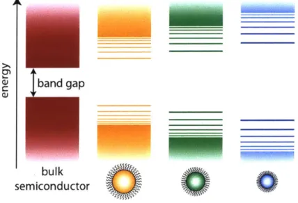
bulk semiconductor
Figure 1.2. Schematic showing the size-dependent band structure.
A typical absorption spectrum for PbS QDs is shown in Figure 1.3. The discrete transitions in a QD are labeled based on analogy to molecular transitions. The lowest energy transition, which is the band gap, is labeled 1Sh-ISe. The ISh and 1Se bands are the valence and conduction bands and are 8-fold degenerate, including spin, in PbS QDs. The second large peak is the lPh-i Pe transition.4 5 The small peak observed between these two peaks in highly
monodisperse QDs is from the spin-forbidden 1Sh-i Pcand I Ph-i Se transitionS.46 Higher energy transitions have been assigned to I Dh- De transitions and other forbidden transitions.47 The broad peak at -500-600 nm has been assigned to a high energy saddle point along the I direction in the Brillouin zone, which acts as a phonon bottleneck, slowing hot carrier cooling to ~1ps-and allowing competing processes such as multi-exciton generation or hot electron transfer to proceed. These excitonic absorption features are sharpest for monodisperse QD ensembles in which the ensemble spectra approach the single QD spectra. In polydisperse ensembles with higher size dispersity, the size-dependent band gap results in QDs with different excitonic energy transitions and blurring of features in the absorption spectrum. By 400 nm, the electronic states
are a continuum of bulk-like states,48 which enable the absorption at 400 nm to be used to accurately measure the QD concentration in mg/mL regardless of the QD size and size dispersity.49
0)h e -2 ip-is 0 he 1 P - .1 P C sU h i
hir
1 1 1P 1.0 1M5 200 2.5 energy (eV)Figure 1.3. Absorption spectrum of PbS QDs in tetrachloroethylene.
1.4 QD Solids: Self-assembly and Ligand Exchange
Several fabrication techniques have been uses to deposit QD solids of varying size and film thickness including drop casting, spin coating, dip coating, spray coating, and assembly at liquid-air interfaces. Many nanomaterials self-assemble into superlattices given sufficient time in a mobile environment such as at a liquid-air interface, but monodisperse PbS QDs self-assemble even in more rapid deposition environments like spin coating.50 Highly monodisperse PbS QDs even self-assemble into superlattices in which all the PbS crystal planes in each QD are aligned throughout the superlattice.50-51
To improve charge carrier transport in QD solids, the long, insulating ligands that provide good colloidal stability during synthesis and storage must be replaced with shorter ligands that reduce the interparticle spacing between QDs. Traditionally, this has been done using a solid-state ligand exchange process in which the spin cast or dip coated solid is immersed in a solution containing the new ligand in a solvent, typically acetonitrile or methanol. Commonly used ligands include short chain organics like 1,2-ethanedithiol (EDT), 1,benzenedithiol (BDT), 3-mercaptopropionic acid (MPA), or 1,2-ethanediamine (EDA), or inorganic ions such as atomic halide ions (Br-, CF , F) or thiocyanate (SCN) . Ligands with lowest unoccupied molecular orbitals (LUMOs) near the conduction band energy have also been used to improve transport.52 Additionally, ligands can shift the energy levels of the QD solid relative to vacuum, enabling band alignment engineering when integrating QD solids into devices.33
Following ligand exchange, the volume of the QD solid contracts, reducing the long-range order and creating cracks in large area films.50 To compensate, devices are usually fabricated using a layer-by-layer deposition approach in which subsequent layers fill in the cracks in previous layers, but these solids have reduced long-range order as compared to films made from a single deposition step.50 To reduce the number of processing steps and improve the superlattice order, solution phase ligand exchanges are being developed by the quantum dot
1.5 Transport in Quantum Dot Solids
1.5.1 Excitons versus
free
carriersIn studying transport in QD solids, one must consider the nature of the charge carriers. Whether they are excitons or dissociated free electrons and holes is determined by the exciton binding energy and the electronic coupling strength between neighboring QDs. In CdSe QDs, the exciton binding energy is large, -0.2- 1.0 eV, depending on the QD size, so charge carriers are excitons under typical experimental conditions.54 In PbS and PbSe, the exciton binding energy is weak, and electronic coupling can be strong in QD solids with short ligands. As a result, photo-generated excitons rapidly dissociate into free carriers at room temperature. Rapid exciton dissociation results in low photoluminescence (PL) intensity in these solids because and electron and hole often do not remain on the same QD for a sufficiently long time for radiative
recombination to occur. The PL intensity increases as temperature decreases (Figure 1.4), revealing that exciton dissociation is a thermally activated process with an activation energy of -35-120meV.55 56 The PL intensity also increases with ligand length, confirming that strong
electronic coupling, which results in fast charge carrier tunneling, also assists in exciton dissociation. The ligand length dependence of the PL intensity is consistent with a tunneling barrier height (see Section 1.5.2) of f-1.
1^',
consistent with values determined for similar alkane ligands with electrical mobility measurements. In device measurements, a charge separation interface, such as the interface with the electron acceptor zinc oxide, or an applied electric field can also assist in dissociating photogenerated excitons into free carriers.61.0 . 0.8 6 0 010 C 0 . S04 40 0.2 fre 0 % carriers, 0.0 0 100 200 300 temperature (K)
Figure 1.4. Normalized photoluminescence intensity as a function of temperature. PL is low near room temperature when excitons rapidly dissociate, and high at low temperatures when charge
carriers remain as excitons.
1.5.2 Charge carrier hopping mechanisms
On the nanoscale, transport in QD solids proceeds via charge carrier hopping from QD to
QD. If the charge carriers are excitons, the hopping mechanism is Frster resonance energy
between the transition dipoles of neighboring QDs. The per QD pair energy transfer rate, kFRET,
is inversely proportional to the donor lifetime (rd) and the center-to-center distance between QDs
(dec)
kET = kFRET = 1 (R)6 (1.3)
Td decc where RO is the FOrster radius and is given by
97PLK 2 FD
(
A (14where ~ ~ ~ ~ R 6P istequnu_ 1281r5n4
J
'(J)A(A)A. 4dA (.4where 7Lp is the quantum efficiency of the donor, 2 is the dipole orientation factor, typically
assumed to be 2/3 for randomly oriented dipoles, n is the refractive index, typically assumed to be the volume-weighted sum of the refractive indices of the inorganic cores and organic ligands,
FD(;) is the donor emission spectrum, normalized to an integrated area of 1, and aA() is the
acceptor absorption spectrum in units of cross-sectional area. Typical values for the F6rster radius are ~8-9 nm in PbS and CdSe QDs.57-59 Exciton lifetimes in CdSe QDs are -15 ns, so the
time between hops (1/kET) is -2-20 ns in CdSe QD solids.57 In contrast, the lifetime in PbS QDs
is -2 ps, so FRET rates are much slower and the time between hops is hundreds of nanoseconds with native oleic acid ligands, and would be expected to decrease only to several tens of
nanoseconds for short ligands.58
If charge carriers are free carriers, the hopping mechanism follows electron tunneling, which has an inverse exponential dependence on the edge-to-edge QD spacing (d)
kE= ktunn oc eJ". (1.5)
The tunneling barrier height, fl, is determined by the QD ligand, with typical values of-2A in vacuum, 0.9-1.2A- for conjugated hydrocarbons, 0.2-0.6^- for highly conjugated chains.60 Reported literature values for charge transport via tunneling in PbS and PbSe QD solids have varied widely from sub-picosecond6' to a several nanoseconds, 62 depending on QD size, ligand
treatment, and superlattice structure.
1.5.3 Temperature dependence of charge carrier hopping
A given QD in a QD solid will typically have neighboring QDs with larger and smaller band gaps as a result of size dispersity in the QD ensemble and the size-dependent band gap. Energy must be conserved in charge carrier hopping processes, so hops to higher energy QDs require additional energy which is provided by the environment in the form of thermal energy. Thus, charge carrier hopping is a thermally-activated process and downhill energy hops are more favorable than uphill energy hops. As charge carriers equilibrate in the solid, they approach a Boltzmann distribution convolved with the density of states, regardless of the initial distribution of excited states. So, following excitation of a random subset of QDs in the solid, the average energy of QDs containing charge carriers will shift to lower energy with time, and the magnitude and dynamics of this redshift, which can be monitored using PL or transient absorption
spectroscopy, gives information about the size dispersity and hopping rate (FRET for excitons, tunneling for free carriers) in the solid, as will be discussed further in Chapter 2. Even if all QDs are the same size, charge carrier hopping may still be thermally activated because the presence of a charge carrier changes the electronic structure of the QD, reducing the band gap by an amount equal to the charging energy, Ec.
The charge carrier hopping rate is strongly dependent on interparticle spacing, so at room temperature, when thermal energy is readily available, hopping is to nearest neighbors (NNH). As the temperature decreases, longer range hops to more energetically favorable QDs become more likely and transport shifts to variable range hopping (VRH). The relevant transport regime can be determined using the temperature dependence of the conductivity, which takes the form:
a = uO exp Z (1.6)
where aO is the conductivity pre-exponential factor, T* is a fitting parameter with units of Kelvin, and z is a parameter that describes the power of the temperature dependence and can be determined from a log-log plot of d(lna)/d(lnT) versus T. Temperature dependence of z=l is an Arrhenius relation and is consistent with NNH with T* = EA/kB. Efros-Shklovskii variable range
hopping (ES-VRH), which arises from the soft Coulomb gap in the density of states created by Coulomb interactions between free electrons,63 is characterized by z=0.5. Mott variable range hopping (M-VRH) is relevant at low density of states when electron correlations are not important, and is characterized by z = 0.25 for three-dimensional transport or z = 0.33 for two-dimensional transport.64 M-VRH has been observed in electrochemically charged CdSe QDs,64 and ES-VRH has been observed in both PbSe 6-66 and CdSe64,67 QDs. The transition from VRH to NNH occurs when the optimal hopping distance is equal to the center-to-center QD spacing. The transition from ES-VRH to NNH in PbSe QDs occurs at 70-100K, with increasing transition temperature for decreasing QD size.66
1.5.4 Experimental transport measurement techniques
Because it is challenging to make direct experimental observations on the nanoscale, macroscale devices and measurements are employed to measure transport properties in QD solids.68 Field-effect transistors (FETs) have been frequently used to measure mobility in QD solids. In an FET, the gate electrode bias shifts the position of the Fermi energy, which can adjust the carrier concentration and fill mid-gap states. High FET mobilities in excess of 10 cm2
V-I s-1 have been measured in QD solids with inorganic ligands.2,69-70 The expected trend of increasing mobility with decreasing ligand length as a result of faster tunneling for shorter inter-particle spacing has been demonstrated through FET measurements.71 They have also been used to measure the temperature dependence of the mobility to understand charge transport
mechanisms.66 FET measurements have shown either increasing mobility with increasing QD size or non-monotonic trends.66, 71-72
While FET devices have many advantages, they measure predominantly electron transport in the accumulation layer at the interface between the QD layer and the gate dielectric and may be impacted by traps at this interface73 and thus may not reflect the three dimensional
QD solid properties. Hall effect measurements can probe the mobility through the film thickness, but they can only be used for high mobility QD solids.74-75 Time-of-flight photocurrent
measurements provide reliable measurements in low-mobility solids, and are transient 76
measurements that are not influenced by long-lived deep trap states.
The time-resolved microwave conductivity technique offers a local probe that measures intrinsic charge carrier mobility.77 Spectroscopic techniques such as ultrafast transient absorption
or photoluminescence also offer a similar complementary view of spectrally resolved charge carrier dynamics in QD solids, and have previously been used to study charge carrier
thermalization'8 and diffusion-assisted Auger recombination in quantum dot solids.7 They can be
used to monitor charge carrier dynamics in energetically resolved states on nanometer length scales, and information on charge carrier hopping can be extracted by fitting the data to a transport model.
1.5.5 Charge carrier delocalization and band-like transport
In an ideal QD solid, free from energetic and spatial disorder, strong coupling will result in mixing between the wavefunctions of neighboring QDs, analogous to atomic bonding in bulk crystalline semiconductors. This wavefunction mixing creates continuous energy bands across the QD solid. Delocalized charge carriers may experience band-like transport similar to bulk semiconductors, rather than incoherent site-to-site hopping via tunneling through insulating barriers between QDs. Claims of band-like transport have been made in CdSe52,69 and PbSe78 QD solids with high mobilities of> 1 cm2 V- s-. As evidence, they cite the observation of increased mobility with decreasing temperature (dy/dT < 0) over some temperature range, rather than the thermally activated behavior expected for a hopping mechanism. However, whether this is sufficient evidence to support the conclusion of band-like transport is the subject of active debate among the community. 68,79-8 The pre-exponential factor in hopping transport
may increase with decreasing temperature. Einstein's relations between mobility and diffusion for a thermally activated hopping process give an expression for the mobility:
ed 2 = ed2
Ea e-fl-EakBT (1.7)
I1hop - 67qopkBT 6hkBT
where d is the center-to center spacing, Ea is the activation energy, I is the edge-to-edge spacing, and/I is the tunneling constant. Thus, for temperatures above T = Ea/kB, hopping transport can
result in mobility that increases with decreasing temperature, and additional evidence is required to claim band-like transport.79
Band-like or metallic transport occurs in metal nanoparticle solids because of the high density of states near the band edge, but semiconductor QDs have much lower band-edge degeneracy (4-fold in PbS and PbSe, singly degenerate in CdSe, without spin).79 When the
degeneracy is high, as in metal nanoparticles, there are many possible conductance channels, so it does not matter if the transmission through each is relatively low. But for semiconductor QDs, band formation occurs only if the transmission is nearly unity, which requires that the coupling energy between QDs is larger than the energy detuning and the natural linewidths of the band-edge states.79 This is unlikely in current QD solids because of variations in confinement energy
(from size dispersity), disorder in coupling strengths (from variation in edge-to-edge spacing), electron-electron repulsion (charging energy), and thermal broadening. Thus, band-like transport
in QD solids is unlikely because of the amount of disorder still present in these materials, and simply showing dp/dT
<
0 over a limited temperature range is not sufficient evidence to prove band-like transport rather than hopping transport.Additional evidence for the possibility of band-like transport is the formation of charge carriers that are delocalized across many QDs. If substantial mixing between wavefunctions of neighboring QDs is present, the charge carriers will be delocalized across several QDs, or even the whole QD solid in the ideal scenario of band-like transport. Thus, researchers measure the localization length of charge carriers using a variety of techniques. Cross-polarized transient grating spectroscopy of CdSe QDs with ln2Te3 ligands suggests a localization length of about 2.2
times the QD diameter.8' Low temperature resistance and magenetoresistance measurements of indium-doped CdSe QD field effect transistors suggested delocalization lengths of several times the QD diameter at high gate voltages.82 Field effect transistors measurements on epitaxially connected PbSe superlattices also reveal a gate-voltage-dependent localization length of-2-3 times the QD diameter for electrons and -1-2 times for holes.83 Transport in the present epitaxial
QD solids follows hopping mechanisms, and reductions in the disorder from QD size dispersity, connectivity (presence of missing connections), and connection width (coupling energy) are needed to increase the localization length and enable band-like transport.83
1.5.6 Trap states
Electronic states that exist within the QD band gap are commonly referred to as trap states and have been the subject of substantial discussion in the literature over the past several years.22,28, 34, 47, 84-96 In particular, trap states have been identified as a limiting factor to
improving PbS QD solar cell efficiencies. Charge carriers are extracted at the lower energy trap states within the band gap, reducing the open-circuit voltage.93'97 Additionally, charge carriers
diffusing in QD solids become trapped in these low-energy states, which act as recombination centers in the solid, and are not extracted as current from the device. The diffusion length is determined not by the diffusivity and carrier lifetime, but by the distance to the nearest trap state.93'98 Thus, the density of trap states is the subject of much interest, and has been measured using a variety of techniques including thermal admittance spectroscopy,34,88,93 field-effect
transistor measurements,85 and photoluminescence measurements,86 and can vary by orders of
magnitude from -0.01 traps per QD for thiol ligands to as low as -104 traps per QD for some halide ligands.8 5