Carbon Nanotube-based Field Ionization Vacuum
Pump
ARC
IVtsby
Daniel .Jang
B.S.. E.E., M.I.T.. 2010
Submitted to the Department of Electrical Engineering and Computer
Science
in partial fulfillment of the requirements for the degree of
Master of Engineering in Electrical Engineering and Computer Science
at the
MASSACHUSETTS INSTITUTE OF TECHNOLOGY
June 2012
@
Massachusetts Institute of Technology 2012. All rights reserved.
. /
Author ..
Department of
Certified by...
.. K- .
...
c...
Electrical Engineering and Computer Science
March 5. 2012
Dr. Luis Fernando VelAsquez-Garcia
Principal Research Scientist
I .
1A
Tesit Supprvsor
Certified by
.Prof. A iintunde Ibitayo ('1ayo) Akinwande
Professor
Thesis Supervisor
Accepted by ...
Prof. Dennis M. Freeman
Masters of Engineering Thesis Committee
Carbon Nanotube-based Field Ionization Vacuum Pump
by
Daniel Jang
Submitted to the Department of Electrical Engineering and Computer Science on March 5, 2012, in partial fulfillment of the
requirements for the degree of
Master of Engineering in Electrical Engineering and Computer Science
Abstract
We report the development of a novel micropump architecture that uses arrays of isolated vertical carbon nanotubes (CNT) to field ionize gas particles. The ionized gas molecules are accelerated to and implanted into a negatively biased getter removing the gas molecules from the volume being pumped.
CNTs are ideal for field ionization because of their nano-sized diameter, high as-pect ratio and of their robust chemical and mechanical structure. The ionizing CNTs are biased at a much higher electrical potential than the gate material surrounding it. Because of the high aspect ratio of CNTs, the area near the tip of the ionizing CNT exhibits very high electric field strength. Gas molecules that are in close proximity to the CNT tips are ionized when electrons tunnel from the gas molecules to the CNT tips. A negatively biased getter positioned nearby attracts the ionized gas molecules, which are implanted in the getter material. With the gas molecules removed from the enclosed space, reduction of the pressure is achieved.
Key challenges in this Field Ionization Pump (FIP) project were the fabrication of high yield working pumps and a high enough ionization current at low voltages. The FIP is designed to evacuate volumes from low vacuum (30 Torr) to mid-vacuum (3 mTorr). We designed the device using electrostatic simulations. Several designs for the FIP ionizers were developed, and we created a device capable of producing field ionization current of 4 nA using an array of 96 field ionizers with 700 V bias voltage at 5 -10-5 Torr. We also show that ion implantation of the ionized atmospheric gas occurs in a silicon getter biased at 1000 V, which is confirmed via X-ray photoelectron spectroscopy (XPS).
Thesis Supervisor: Dr. Luis Fernando Velisquez-Garcia Title: Principal Research Scientist
Thesis Supervisor: Prof. Akintunde Ibitayo (Tayo) Akinwande Title: Professor
Acknowledgments
First and foremost I'd like to thank Dr. Luis Fernando Velasquez-Garcia for all of his dedication and care into guiding me throughout this project. Your expertise in fabrication processes was invaluable in getting this project moving so quickly, and your critical analysis helped me so much in honing my thought process. Thank you Prof. Ibitayo (Tayo) Akinwande for your guidance throughout my graduate student career and instilling in me the importance of looking at the big picture. Your excitement with all that is thought-provoking is very contagious, and I hope to never stop being curious at the world surrounding me.
I would like to thank the MTL staff members for always being helpful when I have
faced hurdles in the processing and planning of the devices. I would like to thank my fellow group members Stephen and Vivi for helping me so much throughout my project. Thank you rest of the group members Michael, Annie, Melissa, Eric, Elle, Kerry, and Alex for your support and rapport - all of you have shown me what it means to be a scholarly student and how to continue to push myself forward.
Last but most definitely not least, I'd like to thank my mom, dad and my brother for always supporting me through the all the walks of my life. I always appreciate your support and advice as they are invaluable to me.
Contents
1 Introduction & Motivation 15
1.1 Chip Scale Micro Vacuum Pump Project ... ... 15
1.2 Overview of the Ion Pumps . . . . 18
1.3 Thesis Organization . . . . 19
2 Background & Theory 21 2.1 Theory of Field Ionization . . . . 21
2.2 Comparison to Electron Impact Ionization and Field Emission . . . . 25
3 Device Structure and Architecture 29 3.1 Horse-shoe (co-planar) Design . . . . 30
3.2 Floral (layer-by-layer) Design . . . . 30
3.3 Self-aligned-gate Design . . . . 31
4 Device Modeling 33 4.1 FEM Electrostatic Simulation . . . . 33
4.2 Estimation of the Tunneling Probability . . . . 36
4.3 Comparison to Previous Work . . . . 37
4.4 Pump Performance Calculations . . . . 40
5 Device Fabrication 45 5.1 Horse-shoe (co-planar) Device Fabrication . . . . 45
5.2 Floral (layer-by-layer) Device Fabrication . . . . 49
5.4 Discussion of the Fabrication Process . . . . 57
6 Electrical Characterization 61
6.1 Field Emission Characterization . . . . 61 6.2 Field Ionization Characterization . . . . 64
7 Summary & Future Work 67
7.1 Thesis Summary . . . . 67 7.2 Suggestions for Future Work . . . . 68
A Mask Layouts 71
B Process Flows 75
C Sensitivity Analysis of the Model 81
D Electrical Characterization of the Horse-shoe Device (10-0) 83
E Electrical Characterization of the Macro Device 87
List of Figures
1-1 A schematic of the Chip Scale Micro Vacuum Pump project . . . . . 17
2-1 A field ionization pump schematic . . . . 21
2-2 Potential well diagram of a molecule going through field ionization . 22 2-3 Potential well diagram of an electron during field emission . . . . 26
3-1 Diagram of the horse-shoe design structure . . . . 30
3-2 Diagram of the floral device structure . . . . 31
3-3 Diagram of the self-aligned-gate device structure . . . . 32
4-1 Axisymmetric Maxwell SV Simulation of a CNT tip with a 30 nm radius with 2 pm aperture radius . . . . 34
4-2 Axisymmetric Maxwell SV Simulation of a CNT tip with a 20 nm radius and 0.4pim aperture radius . . . . 35
4-3 Field strength dependence on distance from the tip for various tip radii 36 4-4 The ionization volume for various tip radii at 1000 V tip bias . . . . . 37
4-5 MATLAB calculation of pump performance with various leak rates 43 5-1 Summarized fabrication steps for the original horse-shoe design . . . . 46
5-2 SEM image of grooves etched on the a-Si layer . . . . 47
5-3 SEM images of Ni nanodots after patterning and etching . . . . 48
5-4 SEM images of CNT creation on the horse-shoe device . . . . 49
5-5 The result of arcing due to exposed oxide layer in the PECVD process for CNT growth . . . . 49
5-7 SEM images of a few pump sites after Ni and TiN etching steps . . . 52
5-8 SEM images of the floral device after CNT growth . . . . 52
5-9 SEM images of the oxide covered CNTs on the floral device . . . . 53
5-10 SEM images of the floral device after CMP . . . . 53
5-11 SEM image of the patterned n-a-Si gate layer . . . . 54
5-13 Summarized fabrication steps for the self-aligned-gate devices . . . . 56
5-14 SEM images of the self-aligned-gate devices . . . . 56
5-15 SEM images of hybrid etching method of Ni . . . . 57
5-16 SEM of an over-etched horse-shoe device during the XeF2 release step 58 5-17 SEM of fabrication issues in the floral and self-aligned-gate structures 59 6-1 A sample electrical test setup . . . . 61
6-2 A picture of a device undergoing electrical testing . . . . 62
6-3 Field emission I-V curve for 10-0 . . . . 63
6-4 The Fowler-Nordheim plot for 10-0 . . . . 64
6-5 Field ionization I-V curve for 10-0 . . . . 65
7-1 Schematic of a sample pump test setup . . . . 68
7-2 Test setup created for pump testing . . . . 69
A-i Mask layout of the horse-shoe design: electrode layer . . . . 71
A-2 Mask layout of the horse-shoe design: nanodot catalyst layer . . . . . 72
A-3 Mask layout of the hose-shoe design: all layers . . . . 72
A-4 The two different aperture radii for the gate structure in the mask layout 73 D-1 Comparison of currents during FE for 10-0 . . . . 84
D-2 Noise test using the electrical test setup . . . . 85
E-1 SEM image of the CNT forrest growth . . . . 88
E-2 Macro test I-V curve of the FE test with the forrest CNTs . . . . 89
E-3 Comparison of the emitted current to the gate/getter current for the FE test with a forrest of CNTs . . . ... . . . . 89
E-5 FI characterization of the forrest of CNTs . . . . 91 E-6 The discolored getter piece after the field ionization run . . . . 92 E-7 I-V curve for the macro FIP test with a forrest of CNTs . . . . 93
List of Tables
4.1 Extracted data from Chen's field ionization tests . . . . 38 4.2 Parameters used in estimating Chen's device performance for field
ion-ization . . . . 39 4.3 Comparison of Chen's device performance estimation and experimental
data . . . . 39 4.4 Sentivity analysis of the non-linear variables in the model . . . . 40
Chapter 1
Introduction & Motivation
1.1
Chip Scale Micro Vacuum Pump Project
Interest in vacuum electronics and their applications has increased in the recent past due to advances in high-frequency amplifiers [1], vacuum fluorescent displays [2], and a variety of sensors such as resonators, infrared sensors and mass spectrometers [3]. These devices require low pressure in order to have long mean free path for electron transport without collisions. Long mean free path is essential for device functionality, sensitivity, and reliability. As these technologies approach smaller scales, the devices find potential application in portable systems where low power consumption is of essence. In order to achieve this, the vacuum pump will also need to consume low power and be integrated with the vacuum electronic device.
In creating such vacuum pumps, several challenges are encountered, as many of the existing technologies are unsuitable for chip-scale integration and low power oper-ation. The industry standard mechanical vacuum pump such as the turbomolecular pumps consume high amount of energy and are quite large as they use multiple stages of rotors in series that require high speeds. This is required in order to continually transfer momentum from the blades to the gas molecules even at low pressure where the mean free path is much longer. Mechanical roughing pumps have been miniatur-ized and have been shown to be successful though it is only able to attain low vacuum levels [4]. The mean free path is of the order of a few microns at this vacuum level,
which is close to the size of the pump chamber, and momentum transfer to the gas molecules is much more reduced resulting in almost no net pressure gradient. In or-der to achieve higher vacuum levels other technologies must be used. Non-mechancal vacuum pumps with no moving parts also exist such as Knudsen pumps and cryop-umps. The Knudsen pump uses a thin channel with a temperature gradient to direct the flow of gas molecules and are micromachined into chip-scale levels; however, the demonstrated terminal pressure is only 0.48 atm [5]. The cryopump cools a surface to below 120 K to freeze the gas molecules thereby creating vacuum and is able to reach ultra-high vacuum (UHV). Several challenges exist in miniaturizing a cryopump as the power requirement in creating such low temperatures is quite high, and thermal isolation is hard to achieve at such a small scale. The cold surface could also saturate quickly when used at low vacuum, therefore cryopumps are typically only used to pump from high to ultrahigh vacuum. A MEMS vapor-jet pump also known as a diffusion pump has also been demonstrated with an ultimate pressure of 370 Torr
[6].
Ion pumps are able to attain UHV levels and could potentially be miniaturized. The ion pump performance is highly correlated with the available surface area
-both the creation of ions and removal of the ions by the getter are highly related to the surface area for both components. Reducing the scale of an ion pump would increase the ratio of the surface area to the pump volume. This will allow for better pump performance. In a macro-scale sputter ion pump, the background molecules are ionized by striking plasma; the ions are sputtered onto a getter which then reacts with the gas molecules and deposit them on the chamber walls. This concept of creating a chip-scale pump with an orbitron pump to sputter ions onto a getter had been proposed [7] and chip-scale sputter ion pumps have been created, though it was
only able to pump from 18 Torr to 17.4 Torr [8].
The Chip Scale Micro Vacuum Pump (CSVMP) project seeks to use MEMS tech-nology to create low-power micro vacuum pumps that will evacuate a small volume down to high vacuum from atmospheric pressure. The pump is divided into several components separated by function as seen in Figure 1-1: the first stage of the pump
Pressure-sensing resonator
Ion pump getters
Electron emitters for electron impact
ionization pump
Field ionizers for field ionization pump
Permanently
sealable valve wo stage
mechanical rough pump
Figure 1-1: A schematic of the Chip Scale Micro Vacuum Pump project. The
mechan-ical rough pump is responsible for pumping down to low-vacuum from atmospheric pressure. The field ionization pump is then responsible down to mid-vacuum level, and the electron impact ionization pump will pump down to the pTorr level.
will be a two-stage mechanical roughing pump to evacuate from atmospheric pres-sure to about 30 Torr. The field ionization pump (FIP) evacuates from 30 Torr to the mTorr range while the electron impact ionization pump (EIIP) lowers the pressure to pTorr levels. MEMS isolation valve will encapsulate the vacuum and a resonator will be used to measure the pressure. The volume pumped will be approximately 20 mm3 while the maximum power usage for the pump will be 1 Watt. The entire pump will take up no more than 2 cm3 of volume, and features MEMS valves to isolate each pumping stage and a resonator to measure the pressure of the chamber. The FIP will bridge the rough vacuum stage and the high vacuum stage, which traditionally re-quired a turbomolecular pump. Demonstrating a FIP that operates at relatively low voltages (in the 1 kV range) has not been possible without a suitable field enhancer to produce the high field strength necessary for FI. CNTs are ideal for MEMS scale FIP implementation as they are conductive, are mechanically robust, and are able to be created in such a high aspect ratio with a sharp tip. MEMS scale ion pumps have not been previously explored in literature, thus this project will attempt to merge
new methods of creating vacuum in this scale.
The micropump can be used in applications such as chemical sensors and mass spectrometer that need low pressure to increase signal-to-noise ratio. The low power specification will allow for sensors to be packaged in a small and portable system.
1.2
Overview of the Ion Pumps
An ion pump can be created at the MEMS scale with slightly different approaches to the macro scale ion pumps. Ions can be created via electron impact ionization (ElI) or by field ionization (FI) and the ions can be buried in a getter via ion implantation.
In ElI electrons are emitted from the tip of the structure due to tunneling when the surface barrier is distorted by the applied electrostatic field. The emitted electrons are accelerated and then collide with the molecules causing them to fragment and ionize. In an ElI pump (EIIP) the molecules then are implanted in a biased getter to create vacuum. It is important to note that since the field emitters are biased at a lower potential, the positive ions that are formed will be attracted to the emitters leading to ion bombardment and tip erosion, especially so at low vacuum [9-13]. Using a second biasing gate to repel these back-streaming ions may help protect the emitters in an EIIP, and for this reason ELI designs are more complicated [14, 15].
In FI a very high field strips the gas molecules of their electrons to ionize them. In a FI pump (FIP) the positively charged ionized molecules will then be implanted into a getter structure that is biased negatively. Gas molecules are removed from the enclosed space to create vacuum. ELI is considered a hard form of ionization whereas FI is considered to be a soft ionization method. Though the ElI method will require about an order of magnitude lower electric field strength than field ionization, it pro-duces more fragmented ions [16, 17]. For this reason FI and a similar phenomenon of field desorption (FD) have received a lot of attention in the field of mass spectrome-try since the mass of the molecules stay intact. Though popular from the mid-1970s to the 1980s FD and FI eventually gave way to other forms of ionization such as fast-atom bombardment and electrospray ionization for mass spectrometry use [18].
Unique capabilities of using FI for mass spectrometry have been discovered recently in the past decade [19-21]. Several methods of microfabrication exist to create a field ionizer such as using protrusions on a razor blade [22], vertical ZnO nanowires [23], vertically isolated CNTs [24], and whiskered silicon nanowires [25]. The ionizing tip on an FI device does not go through ion bombardment and tip erosion since the ionized molecule with a negative charge is repelled by the positive tip. FI devices therefore should be suitable for higher pressure operation compared to EII sources . In the CSVMP project the EIIP will pump from mid-vacuum to high-vacuum. The FIP does not need such high vacuum levels to operate and therefore will be used to reach mid-vacuum levels. It will act as the second stage of the pump and will be the focus of this project.
1.3
Thesis Organization
The motivation for this project and a brief overview of the existing pumping tech-nologies were described in Chapter 1. In Chapter 2 the fundamental theory of field emission and field ionization is discussed. Understanding these phenomena and how they relate to the device geometry is crucial in selecting the device architecture and designing the device for optimal performance and ease of fabrication. In Chapter 3 we present the device structures for the FIP we investigated in this thesis. Chap-ter 4 presents the results from electrostatic simulations and estimation of the FIPs performance. Chapter 5 covers the fabrication of the devices. Chapter 6 analyzes and discusses the electrical characterization done on one of the test devices. Lastly, Chapter 7 summarizes the work done, the results and recommendations for future work including the types of tests needed to verify the pumps operation.
Chapter 2
Background & Theory
2.1
Theory of Field Ionization
In field ionization a strong electric field is applied between the tip and the gate of the device, which causes the potential barrier between the tip and the gas molecules to deform, leading to electrons tunneling from the gas molecules into the tip. The molecules that lost electrons are now ionized, and they are accelerated to a getter that is negatively biased and embedded in the getter.
Getter V V+ loni Tip
Ground
Figure 2-1: A field ionization pump schematic
The field ionization process can simply be put as
(2.1) where M represents the gas phase molecule that is ionized.
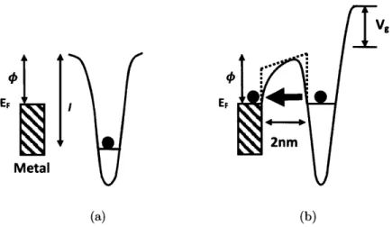
EF E,
2nm Metal
(a) (b)
Figure 2-2: Potential well diagram of a molecule going through field ionization: (a) undistorted (b) in a strong field gradient biased by V. The valence electron of the molecule is raised to the Fermi level and tunneling may occur. The trapezoidal approximation of the barrier is shown.
Ionization energy I is the minimum energy required to remove an electron from a molecule, and it is analogous to the work function
#
for metal. This represents the energy required to remove the outermost electron from the molecule. When an electric field is applied to a gas molecule, the potential barrier deforms from its unperturbed state. With a high enough field, the potential barrier will deform and allow electrons to tunnel through the finite barrier width. The process is defined as field ionization. The energy level of the electron in the gas molecules must be elevated above the Fermi level of the tip material for electrons to tunnel into the tip. Figure 2-2 shows how the potential well of a molecule is deformed during field ionization.Note that CNTs have a work function of about 5 eV [26, 27]. If the molecules are too close to the tip ionization will not occur due to the absence of empty states below the Fermi level [28]. If the tip is too small the tip may burn out due to Joule heating from the high current, and if the tip is too large the tip will not create a sufficiently high field for field ionization.
field is applied at the tip that will result in all of the gas molecules near the tip to be ionized. In this strong-field regime the ion current is limited by the amount of un-ionized neutral gas molecules near the tip and hence it is said to be supply-limited. The number of molecules going into this ionization zone is directly proportional to the pressure of the chamber. The ionization current is expressed as
Ii = q - - -C - A v (2.2)
kT
where q is the electron charge, P is the pressure, k is Boltzmann's constant, T the temperature in kelvin, C is the thermal speed of the molecule, and A is the cross sectional area of the ionization sphere.
Another possibility is the barrier-limited ionization that occurs in the low-field regime. In this case only the gas molecules very close to the tip will have sufficient probability of being ionized. The ion current will depend on the number of molecules near the tip and the lifetime of the molecules (r). The lifetime depends on the frequency at which the electrons arrives at the potential barrier (f) and the tunneling probability (D) where r = -L. With this, the current for field ionization has been modeled by Gomer [28] to the first-order as
Ii= q. - - v .
f
.D (2.3)kT
where v is the ionization volume,
f
is the barrier attempt frequency and D ex-presses the tunneling probability. Gomer uses the expectation value of momentum p, and effective radius re for the s-state orbital to estimate the arrival rate of electrons at the barrier asf
= pe/ (2mre) (2.4)The barrier attempt frequency
f
is estimated to be in the order of 10" to 1016 sec-1 [28, 29]. There is a minimum distance between the ionizing metal surface and the molecule. If the molecule is too close to the surface, ionization would not occur due to the absence of empty states below the Fermi level. This critical distance Xc isXc
1
(2.5) As the distance between the molecule and the tip grows, the barrier width also grows, which decreases the tunneling probability D. The tunneling probability is ap-proximated using the trapezoidal area formed between the metal tip and the molecule using the Wentzel-Kramers-Brillouin (WKB) approximation asDWKB = exp (-2(2m/h2)1/2 j (V - E)1/2dx)
exp -2B
40+
±/ X( dx)= exp
-
.
(13/2 _ 03/2) (2.6)where m is the electron mass, h is the Dirac constant, V is the potential en-ergy of the electron, E is the kinetic enen-ergy, I is the barrier width, B = 6.8 -io7 [VeV-3/2cm-1], I is the ionization energy of the gas molecule,
#
is the work function of the metal tip, F is the applied electric field. The barrier has been approx-imated as a trapezoid with side heights of I and4
as seen in Figure 2-2 [28, 30].The electric field F can be modeled as
F = eff - VG (2.7)
#eff oc r- (2.8)
where
#eff
is the field factor that is dependent on the tip geometry, r is the radius of the tip, and VG is the voltage applied at the tip. The field factor depends purely on the physical structure of the device. There is a high dependence of the field factor - therefore the electric field - on the tip radius, which makes the high aspect ratio and sharp CNTs a good choice for creating the tip structure.assume that the tunneling probability becomes significant when the barrier width is 1 to 2 nm, which is in the order of the de Broglie wavelength of an electron. The barrier width reduces to this size when a field strength of the order of 1 -108 V/cm is applied to the metal surface [31]. Gomer was the first to observe that a field strength of about 108 V/cm was needed to field ionize hydrogen molecules [28]. Hydrogen (H2)
has an ionization potential of 15.43 eV which is close to the ionization potential of the atmospheric gasses such as oxygen (02), nitrogen (N2), argon (Ar) and carbon dioxide (C0 2) at 12.08 eV, 15.58 eV, 15.76 eV and 13.79 eV respectively. In this thesis 1 -108 V/cm will be used in estimating the ionization volume where the gas molecules will tunnel with probability D.
2.2
Comparison to Electron Impact Ionization and
Field Emission
Electron impact ionization is a form of ionization where energetic electrons collide with molecules to ionize them. This ionization can be represented as
M + e~ 7 M+ + 2e- (2.9)
where M represents the neutral gas phase molecule that will be ionized. Both M+ cations and M- anions are produced, though the ratio of cations to anions ranges from 102 : 1 to 104 : 1 because cation formation from a neutral molecule by electron impact is a much more efficient process than an anion formation by electron capture [31, 32]. Electron impact ionization therefore can be seen as a two-step process where the first step is the creation of electrons to be used in the reaction and the second step of accelerating those electrons to the molecules to ionize them.
Figure 2-3 shows the potential diagram of the field emission phenomenon.
The Fowler-Nordheim (FN) equation describes the current density due to field emission. As a function of the bias voltage, the current is described as
Lowered potential well due to the electric field
EF
1-2 nm
Metal Vacuum
Figure 2-3: Potential well diagram of an electron during field emission
I = aFNV2e-FN
(2.10)
where
aAf 2 B(1.44.10-7) 0.95B03/2
aeFN =1.14
eXp
, 1bFN =
0and A = 1.54 -10-6 AV- 2eV-1 and B = 6.87 -107 VeV- 3/2cm-1. a is the effective emitter area, > the workfunction and
#
is the field factor.Equation 2.10 can be rearranged to
ln
(I/V2)
= In (aFN) - (2.11)V
which shows that ln (I/V 2) varies linearly with 1/V by a factor of bFN, from
which
#
can be extracted.In the ElI process, the field emitted electrons are accelerated above the ionization potential of the gas molecules. Only some of these electrons are able to ionize the neutral molecules. The ratio of the ion current to the emitted electron current is defined as the ionization efficiency, and is described as
I
1(E)
= p - L - UTot(E) (2.12)IE (E)
where I,(E) is the ion current, IE (E) is the electron current, p is the molecule density in the chamber, L is the collision pathlength, and
o-(E)
is the total ionization cross section, which is a measure of the probability that a given ionization process will occur when a molecule interacts with an electron. To eject the outermost electron of a molecule, the field emitted electron must have higher energy the ionization potentialof the outermost electron. The total ionization cross section increases as the electron energy increases, and is maximized when the electron has the same energy as the outermost orbiting electron. Any further increase in energy decreases the ionization cross section due to the shortened interaction time between the electron and electrons of the gas molecule [33].
Chapter 3
Device Structure and Architecture
Two broad design architectures were explored in this project. The second architecture was created to improve on the first. Arrays of carbon nanotube (CNT)-based devices were used in both.
Ever since CNTs were first reported in 1991 [34], their extraordinary mechanical, electrical and thermal properties have made them a topic of interest for many research applications [35-37], in particular in field emitter arrays (FEAs) [38-42]. CNTs are chemically and mechanically robust, and are well suited for device fabrication pro-cesses that require high temperature steps after the CNT growth. CNTs high aspect ratio and sharp tips provide the high field factor needed for high electric field strength and therefore field ionization.
The initial device architecture used a horse-shoe shaped design, where the gate and tips were both comprised of CNTs. Surrounding and equidistant from the ionizing tip
CNT would be the gate CNTs used to bias the tip CNT. This design exhibits a highly
transparent ionizing tip allowing for higher chances of ion creation. The surrounding gate structures are also created with CNTs. After fabrication issues were discovered with this approach, the design was modified into a design with a layer-by-layer ap-proach that resembles a floral shape - a central high-field aperture surrounded by neutral flux apertures - and another that uses a self-aligned gate method of defining the gate aperture. This layered approach allows for more consistency during the fab-rication process and exhibits a higher field factor compared to the horse-shoe design.
Both approaches are detailed in the following sections.
3.1
Horse-shoe (co-planar) Design
The proposed design called for vertically aligned CNTs to make up the gate and the tip portion of the device. The gate CNTs would all have the same potential while the tip would be set to a different potential to create the electric field. Using CNTs for the gate structure allows the gas molecules to reach the tip to be ionized with high transparency, which increases the flux of neutral molecules to the ionization region.
The proposed design is shown in Figure 3-1.
Apertu re radius
CNT height
(a) (b)
Figure 3-1: The original horse-shoe design of one field ionization pump. The tip and the gate structures are all comprised of CNTs. (a) A single pump structure (b) arrangement of the array
The distance between the tip and the gate is 2 pm for half of the devices, and the other half 3 pm, as seen in the mask layout in Appendix A.
3.2
Floral (layer-by-layer) Design
The second design for the FIP allows for a simplified and more reliable fabrication process. The main structural difference compared to the original design is that the silicon substrate acts as one of the electrodes and is electrically connected to the ionizing CNT tip. The tips are arranged in a hexagonal array with 5 pm pitch to
allow sufficient separation between each unit. The gate structure is not comprised of several CNTs but rather a flat layer of n-type amorphous silicon (n-a-Si), which is electrically isolated from the substrate by a layer of oxide. This gate structure resides in the same plane as the ionizing tip and has an aperture opening in which the tip is centered. The floral shape comes from additional holes made on the gate to allow gas molecules to gain greater access to the ionizing tip. The aperture radius is 0.4 pm to maximize the field factor.
Note that as the device specification requires the use of voltages of up to 1 kV, a minimum thickness of oxide will be needed between the substrate and the gate electrode. Assuming a maximum dielectric field strength of 300 V/pm for PECVD oxide, around 3pLm oxide will be needed to separate the two conductive layers. This
also necessitates the CNTs height to be at least 3 pm.
cNT n-a-Si
(a) (b)
Figure 3-2: Diagram of the floral device array: (a) top view (b) cross-sectional view
3.3
Self-aligned-gate Design
An even more simplified design using self-aligned fabrication methods was explored in addition to the floral shape design. This self-aligned-gate design would eliminate the need to use photolithography to define the gate aperture, a process that requires the utmost precision and can be inconsistent between different device wafers. The layer-by-layer approach is still preserved and a layer of oxide separates the two conducting
layers. The aperture radius is determined by the amount of oxide deposition, and therefore is increased to approximately 1 pm.
CNT
(a)
n-a-Si
(b) Figure 3-3: Diagram of the self-aligned-gate device array: sectional view
cross-Chapter 4
Device Modeling
As stated in Equation 2.3, the ionization current in field ionization in the low-field limit can be modeled to first order as
(P)
I =q* - -- v -f -D
We need to estimate the ionization volume (v), the barrier attempt frequency (f) and the tunneling probability (D), and assume a pump volume and leak rate to forecast the pump performance.
4.1
FEM Electrostatic Simulation
In order to estimate the ionization volume, the devices were modeled using electro-static Finite Element Method (FEM) simulations via COMSOL and Ansoft Maxwell
SV. FEM simulations are useful for electrostatic calculations as they are able to
handle complex geometries and boundaries while reaching accurate results through convergence. A result of such simulation using Maxwell is seen in Figure 4-1.
The dependence of field factor on the various parameters such as the radius of the tip, distance between the gate and the tip, height of the CNTs was analyzed to find the field factor that is characteristic of the design.
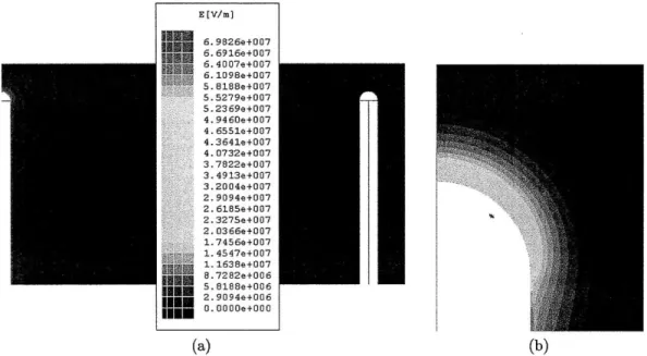
Simulations were first run for the horse-shoe design. 1 pm tall CNTs with 40 nm tip radii and 1p m distance between the tip and the gate produced a field factor (#) of 1.5 - 105 cm-- 20 nm from the surface of the tip. In this case, since F = VG -
#,
less than 700 V would be needed to be applied to the tip in order to achieve a field strength of 1 - 108 V/cm required for field ionization. The voltage required for field ionization is shown to be heavily dependent on tip radius and to a lesser degree on other geometric factors (such as height of the CNTs and gate aperture radius), which will vary within the array due to variations exhibited during the fabrication process. This initial simulation run showed that the horse-shoe design would yield a feasibleFIP. E [V/ml NO6.9B26e+007 6. 6916e+0 07 6. 4007e+0 07 ' 6~109~8e+007 5 .5279e+0 07 5.2369e+007 4 .9460e+007 4 .6551e+0 07 .641e+07-4:.0732e+ 07 3 .7822e+0 07 3 .4913e+007-3.2004e+007 2.9094e+00? 2 .6185e+0 07 2 .3275e+0 07 2 .0366e+0 07 1.7456e+007 1. 4547e+0 07 1.1638e+007 8.7282e+006 5.8188e+006 2. 9094e+006 IS 0.0000e+000 (a) (b)
Figure 4-1: Axisymmetric Maxwell SV Simulation of a CNT tip with a 30 nm radius with 2 pm aperture radius at 1 V andfor the horse-shoe design: (a) the entire test
setup (b) close-up of the tip
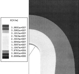
For the updated floral and self-aligned gate designs a more exhaustive modeling was done to characterize the field strength and its dependence on the distance from the tip as well as the tip radius. The two designs share similar features and geometries for the gate and the tip that both simulations were done together. The most noteworthy difference in design compared to the horse-shoe design is the reduced aperture radius of less than a micron and the increased height of the CNTs to 3 pm. Figure 4-2 shows
a simulation run done for a 40 nm radius tip with a 0.4 pm aperture radius. E[V/M] 3.9891e+007 3.5902e+007 3.1913e+007 2.7924e+007 2.3935e+007 1.9946e+007 1.5957e+007 1.1967e+007 7.9783e+006 3.9891e+006 0.0000e+000
Figure 4-2: Axisymmetric Maxwell SV Simulation of a CNT tip with a 20 nm radius and 0.4 pim aperture radius at 1 V
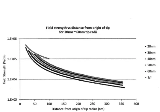
The red line originating from the middle of the tip shows the direction along which the electric field was measured. The simulations were run with tip height of 2pm, gate aperture radius of 0.4 pm for various tip radii. Summary of the field strength dependence on distance and tip radius are shown below in Figure 4-3.
The highest field strength was achieved with the smallest tip radius of 20 nm. To approximate Gomers field factor in Equation 2.8, 1/r is also plotted, which is closely matched by the maximum field strength calculated using FEM.
To simplify the estimation of the ionization volume, low-field regime for field ionization was defined as any area above 1 - 108 V/cm. The ionization volume for one ionizing tip was estimated to be the volume of half of a sphere with radius at which field ionization can be achieved with 1000 V bias voltage less the tip volume.
I/ 1
.4
.7r. ( - r 3)(4.1)
Though the 20 nm tip was able to achieve higher electric field strength using the same bias voltage, the field strength diminished too quickly for its ionization volume
Field strength vs distance from origin of tip for 20nm ~ 60nm tip radii
0 50 100 150 200 250 300 350 400
Distance from origin of tip radius (nm)
Figure 4-3: Field strength dependence on distance from the tip for various tip radii. The tip is biased at 1 V and the gate aperture radius is 0.4 pm. The distance is measured from the origin of the tip radius. Note that there is no electric field inside the conducting tip.
to be the highest. Summary of the ionization volumes compared to tip radius can be seen in Figure 4-4.
4.2
Estimation of the Tunneling Probability
The calculation of the tunneling probability (D) is quite complex due to the nature of the wave equation. WKB approximations are used to find an estimate. The analytical approximations of the tunneling probability was described in Equation 2.6, and is as follows: DWKB eXp (- . (13/2 _ 3/2) 1.E+06 1.E+05 1.E+04 1.E+03 * 20nm * 30nm * 40nm * 50nm * 60nm * 1/r
Ionization Volume vs Tip Radius 4.0E+05 E -3.7E+05 3.6E+05 3 3.OE+05 E+3.5E+05 O 2.2E+05 2.10E+05 0- 1.0E+05 -1.4E+05 0.OE+00 0 10 20 30 40 50 60 70 Tip radius (nm)
Figure 4-4: The ionization volume for various tip radii at 1000 V tip bias
where B is a constant of 6.8
-107
VeV-3/2cm-1/2, I is the ionization energy of the molecule in eV,#
is the work function of the cathode in eV, and#
- V, the electric field strength in V/cm. As mentioned in Chapter 2, CNTs work function is around 5 eV, and the ionization energy of N2 is 15.58 eV, 02 is 12.08 and Ar is 15.76 eV.Using Equation 2.6 the tunneling probability for different atmospheric gases are calculated for field strength of 2. 108 V/cm, which is attainable with 1000 V bias and 40 nm tip radius: for N2 the tunneling probability is 1.11. 10-7, for 02 3.17-
105
and for Ar 8.24. 10-8. As N2 is the most abundant atmospheric gas by far, D = 1. 10-7will be used for the purposes of estimating the pump performance with bias of 1000 V for 40 nm tip radius structures.
4.3
Comparison to Previous Work
Data from previous work was compared to our model to estimate the performance we could expect from our device and gauge the accuracy of our model. Field ionization arrays were previously tested by Chen, where her field emitter array was tested in field ionization mode in two different pressures of Ar [24]. The data for the ioniza-tion current has a low magnitude and with a wide spread, so four data points were
Table 4.1:
Tip Voltage 500 V 570 V
P (Torr) I (Amps) I (Amps)
8.5e-4 3e-12 1.0 e-11
5.6e-3 1.5e-11 1.5e-10
Extracted data from Chen's field ionization tests
extracted at the extremes and are summarized in the following table.
Our previously estimated electrical characteristics can be compared to this data to validate our model. Note that for any given bias voltage - and therefore a fixed ionization volume - the ionization current should be directly proportional to the pressure, though this is not the case in this experimental data. The ratio of pressures is 6.6, though the ratio of the currents is 5 with 500 V bias and 15 with 570 V bias. Although this shows some intrinsic limitation of fitting this experimental data to our modeling, this comparison will be used to coarsely validate our model.
The ionization volume was derived from Chen's estimate of her tip radius at 20 nm and matching it to our simulation results on the ionization volume. A conservative estimate of 1015 sec-1 is used for the barrier attempt frequency. Tunneling probability is calculated for Ar, the gas used for her experiment. The field factor, which is solely based on the device geometry, is taken from her experimental data and is around
5 -105 cm-1 for the 10x1O arrays used in her test. From this, the field strength at the CNT-vacuum boundary is calculated for the two different biases used in the experiments, which is then used to calculate the tunneling property using Equation
2.6.
The array size is estimated by assuming a yield of 30% on her 10x1O size array used for the field ionization test. Using these parameters and our best assumptions of Chen's devices we estimate the ionization current her devices would exhibit using our model.
In estimating how Chen's device would perform, the parameters in Table 4.2 were used. After estimating the values that Chen's device would have exhibited, comparison was done to her experimental ionization current data, which is shown in Table 4.3.
500 V 570 V Assumptions
Ionization volume per tip (v) 2.8 -10-17 cm3 4.0- 1017 cm3 r = 20nm
Tunneling probability
(D)
8.0- 10-6 3.4-104
# = 5-
105cm-1Barrier attempt frequency
(f)
1015sec-Array size 30 30% yield
Table 4.2: Parameters used in estimating Chen's device performance for field ioniza-tion
Estimation of Chen's device performance Chen's data
Bias 500 V 570 V 500 V 570 V
P (Torr) I (Amps) I (Amps) I (Amps) I (Amps)
8.4e-4 2.9e-11 1.2e-10 3.0e-12 1.0e-11
5.6e-3 1.9e-10 8.le-10 1.5e-11 1.5e-10
Table 4.3: Comparison of Chen's device performance estimation and experimental data
Our calculation overestimated Chens device performance by a factor of 5.4 to 12.7, within an acceptable range of error. This difference can be attributed to our conservative estimation of the ionization volume and barrier attempt frequency, the number of working devices in Chens device array, and the estimation of the tunneling
probability.
To better understand the variation between our model and Chens experimental data and gain insight into our models dependence on individual parameters, a sen-sitivity analysis was done for each of the non-linear variables. The full analysis is shown in Appendix C, and the summary is shown below:
For all of our models we assume the average gas temperature to be 300 K. This can vary due to the heating of the ionizing tips which may raise the gas temperature, or lower due to pumping of the chamber. The ionization current is inversely proportional to the temperature.
The ionization volume can vary due to the variation of the CNT tip radius. As seen in Figure 4-4 the variation of the tip radius had a limited effect on the ionization volume. The sensitivity analysis for radius was done for the 20 nm, 30 nm, and 40 nm tips with bias of 500 V.
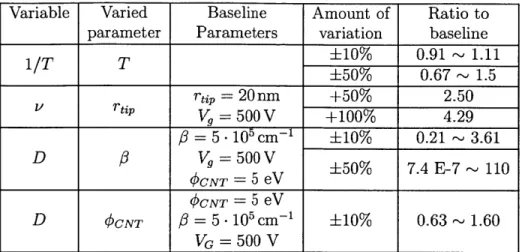
Variable Varied Baseline Amount of Ratio to
parameter Parameters variation baseline
1/T T
±10%
0.91 - 1.11 ±50% 0.67~ 1.5 T tip = 20nm +50% 2.50 V = 500V +100% 4.29 = 5- 105 cM-1 t10% 0.21 ~3.61D
#3
Vg=500 V
D VgT
5eV
&50% 7.4 E-7 ~ 110#CNT
=5 eV
#CNT
= 5 eVD
#CNT#
= 5-
105 cm-1 +10% 0.63 1.60VG=
500 V
I
I
Table 4.4: Sentivity analysis of the non-linear variables in the model
be underestimated by as much as a factor of 10. A more thorough analysis of f is omitted from this thesis due to its complexity depending on the gas element and orbital of the outer most electron.
Our model for the ionization current is highly sensitive to the tunneling probability D, which is somewhat sensitive to the CNT work function
#CNT
and highly sensitive to the field factor#.
This is as expected due to the exponential relationship that the work function and field factor have on the tunneling probability as seen in Equation2.6. Chen's experimental data - which had a deviation factor of 12.7 from the model
- is within the error bounds of this analysis using the lowest amount of variation
(+10%, except
+50%
for radius) which yields a deviation factor of 16. For a more accurate model, an accurate estimate of the field strength near the ionizing tip as well as the work function of the CNT is needed.4.4
Pump Performance Calculations
In order to model the pump performance, we assumed that all of the ionized molecules are implanted into the getter and there is neither charge recombination nor neutral-ization. The ionization current is directly proportional to the chamber pressure, as stated in Equation 2.3, which means that the pump rate is directly proportional to the chamber pressure.
dP
_
dN, kT)
(4.2)dt
dt
constant volumnedN
=NNt
= -ci - N (4.3)dt
V
ci - -f
- Dwhere N is the number of molecules in the chamber, v is the ionization volume,
V is the chamber volume. From here we add the effects of leakage, which can be
estimated as
Q -Patm+
Or
-As
Nik = kT(4.4)kT
where Nik represents the leakage rate in molecules per second,
Q
is the leak rate at standard conditions, 0r is the outgassing rate and A. is the surface area of the chamber. Leakage will result from the chamber ports and valves. Outgassing will primarily result from desorption from the chamber walls and bulk. Combining the pumping and leakage rate we getdN
-
=Nt
+gin
= -c1 - N + 9k (4.5)Solving the differential equation, we get
N(t)
=No
-- e-lt + --(4.6)
V 1
Nt-i - = --k
(4.7)
ci v f -(D
In order to reduce the terminal pressure of the pump, the leak rate must be minimized and the ionization volume maximized.
Pump performance was estimated using MATLAB. The following assumptions were made:
Chamber volume 20 mm3 Initial pressure 30 Torr
Ionizing tip bias 1 kV
Ionizing tip radius 40 nm Pump array size 50,000 field ionizers Barrier attempt frequency 10" sec-1
Tunneling probability i0-7
The chamber volume was chosen as a volume that a chip scale vacuum pump would be expected to pump. Tip radius of 40 nm is chosen, which is the radius exhibited by most of our CNTs. The barrier attempt frequency is a conservative estimate, and the tunneling probability assumes a field strength of 2 -108 V/cm, attained at the surface of the 40 nm radius tip with 1000 V bias. An array size of 50,000 is equivalent to an array area of 1 mm2 with 5 pim pitch between the ionizers. The ionizing tip bias voltage and tip radius were used to determine the ionization volume per tip, which is calculated to be 3.7 -10-16 cm3. The result of pumping performance calculation is seen in Figure 4-5. The leak rate should remain between 1 - 10-8 cm3 and 1 -10-9 cm3 in order to reach mTorr level using a FIP with array size of 50,000.
2
10
101
10
10~
Pumping rate for the Field Ionization Pump
array of 50000
Increasing
1 U1104-10
0
200
400
600
800
Pumping Time (second)
1000
Figure 4-5: MATLAB calculation of pump performance with various leak rates
0
Chapter 5
Device Fabrication
5.1
Horse-shoe (co-planar) Device Fabrication
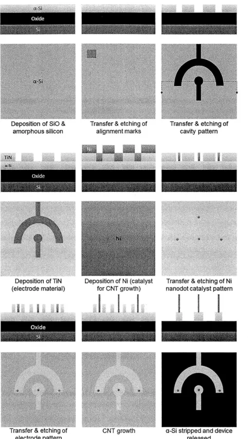
The devices were fabricated in MITs Microsystems Technology Laboratory (MTL). A summary of the process steps for the horse-shoe device is shown below in Figure 5-1. We start with an n-Si wafer and the standard photolithography methods are used to pattern the alignment marks, which is then plasma etched. The alignment marks will aid in aligning the Ni catalyst nanodot patterns onto the horse-shoe looking TiN layer. After the alignment marks are etched, the photoresist is ashed, and the wafer goes through a RCA clean. 3 pm of oxide and 50 nm of amorphous silicon (a-Si) are deposited onto the wafer. The oxide isolates the substrate from the conductive TiN layer. The a-Si layer was an attempt at curbing the arcing problem during the PECVD step for CNT growth by shielding the oxide layer. Standard photolithography steps are used to pattern the grooves so that the TiN layer can be anchored to the oxide beneath. The a-Si is plasma etched until the oxide is exposed and the photoresist is ashed away. A SEM image of the device at this stage is seen in Figure 5-2.
Deposition of SiO & Transfer & etching of amorphous silicon alignment marks
Deposition of TiN (electrode material)
Transfer & etching of cavity pattern
Deposition of Ni (catalyst Transfer & etching of Ni for CNT growth) nanodot catalyst pattern
I
I
I
I
I
I
i ranster ot eteniing o1
electrode pattern swippea ana aevicereleased
The wafer at this point goes through a pre-metal clean, and 50 nm of TiN is sputtered via physical vapor deposition (PVD) and 20 nm of Ni is deposited through e-beam evaporation. The TiN layer is the conductive layer that the test setup probe will contact in order to establish the tip and gate potentials. Ni acts as the catalyst for the CNT growth step.
Figure 5-2: The device after the grooves are etched on the a-Si layer
The Ni nanodots are patterned using standard photolithography. These nanodots have a diameter of 0.6 im. The Ni layer is then wet etched using Transene Ni etchant. This step introduces the most amount of variability in the entire fabrication steps as over-etching could result in no CNTs growing, while under-etching will result in too many CNTs growing from each of the isolated Ni nanodots. The wet-etch is done in an ultrasonic bath which controls the temperature of the bath and can aid in the etch process with the ultrasonic mixing. It was found that the etch rate varied significantly depending on the temperature. The temperature of the bath is set at 27 *C and the ultrasonic level is set at 7 out of 10. Another metric is introduced to establish the correct amount of wet etching. After between 4 to 6 minutes of etching in this condition it is seen that the device wafer goes through a color change as the Ni layer is removed. The TiN layer underneath has a brilliant gold color as the Ni layer is almost completely depleted. This color change transition takes around 7 seconds. The wafer is left to continue to etch 5 more seconds after the color change has subsided, after which it is promptly rinsed with DI water. The photoresist is
ashed. A SEM image of the wafer at this point is seen in Figure 5-3.
With much of the TiN exposed, the electrical layer is then patterned. This layer looks very similar to the grooves made earlier in the n-a-Si layer, only slightly larger to cover the exposed oxide before the CNT PECVD step. Using standard photolithog-raphy steps again, the TiN layer is patterned and plasma etched until the a-Si layer is exposed. After the photoresist is ashed the wafer goes through CNT deposition.
The PECVD step for the CNT growth is done at 750 'C for 15 minutes to achieve around 2 pm of height for the CNTs. At this point the device resembles that of the final device. The a-Si layer is then etched away with XeF2 and the device is released
and ready to be tested. SEM images of the device at this step can be seen in Figure
5-4.
(a) (b)
Figure 5-3: Ni nanodots after patterning and etching. The left picture is of a test wafer that only shows the Ni nanodots while in the right the groove made in the a-Si layer can also be seen.
It is important to note that the a-Si was not able to consistently shield the oxide layer from being exposed to the PECVD process for CNT growth. The result is that arcing occurs that would char the surface of the devices and render them useless. Optical microscope images of the resulting devices are seen in Figure 5-5. Many avenues of fixing the problem was explored such as pulsing the plasma of the PECVD to varying the height of the a-Si providing a conducting path to the a-Si layer to ground in the CNT reactor. As not all devices were charred due to the arcing, some were usable, though the integrity of the oxide layer was often compromised due to
(a) (b) (c)
Figure 5-4: (a) CNTs are seen on a test wafer with no TiN or n-a-Si layer. (b) a device layer with CNTs grown on the TiN layer. The horse-shoe design is clearly seen. (c) Close-up of a device with taller CNTs
the arcing. Though a few devices were completed and even made it to the electrical testing phase, the problems associated with the fabrication of the device resulted in subsequent exploration of a new design to improve the fabrication steps, obtain more robust and fail-proof devices as well as improving the performance of the pumps.
Figure 5-5: The result of arcing due to exposed oxide layer in the PECVD process for CNT growth
5.2
Floral (layer-by-layer) Device Fabrication
The arcing issue seen in the previous designs fabrication was eliminated in a new design scheme that requires no oxide layer to be deposited before the CNT growth. The CNTs are electrically connected to the Si substrate itself, which now acts as one of the two electrodes to bias the ionizing tip.
CNTs grown on substrate Oxide deposition Planarization of oxide through CMP
Cn-a-Si
n-a-Si deposition as gate Patterning of gate openings BOE etch to release device material
Figure 5-6: Summarized fabrication steps for the floral-design device. Note that the CNTs are positioned on top of TiN pads omitted in the figure. The pads act as a diffusion barrier between Ni and the substrate.
The fabrication steps for this device are summarized in Figure 5-6. To create this device we start off with a blank n-Si wafer. Standard photolithography is used to pattern the alignment marks, which will later aid in aligning the aperture holes on top of the CNTs as well as patterning the gate for device definition. The alignment mark is plasma etched for 180 seconds. After the photoresist is ashed the wafer is Piranha cleaned to prepare for TiN and Ni deposition. 50nm of TiN is sputtered via PVD. This layer will act as the diffusion barrier to the Ni layer and will aid in the CNTs gaining a solid physical and electrical connection to the substrate. The TiN layer undergoes rapid thermal anneal (RTA) at 800 'C for 30 seconds in order to lower resistivity, and increase film density. [43] After this step the TiN layer changes its color from dark gold to bright gold, which improves the visual cues needed during the Ni wet etching step. After the anneal step, 20 nm of Ni is deposited through ebeam evaporation. Ni is used as a catalyst for the tip-growth mechanism through which CNTs are grown. Standard photolithography is used to pattern the Ni nanodots. These nanodots have a diameter of 0.6 pm. The Ni layer is then wet etched using Transene Ni etchant. This step introduces the most amount of variability in the fabrication steps as over-etching could result in no CNTs growing, while under-etching will result in too many CNTs
growing from each of the isolated Ni nanodots. The wet-etch is done in an ultrasonic bath which controls the temperature of the bath and can aid in the etch process with the ultrasonic mixing. It was found that the etch rate varied significantly depending on the temperature. The temperature of the bath is set at 27 *C and the ultrasonic level is set at 7 out of 10. Another metric is introduced to set the correct amount of wet etching. After between 4 to 6 minutes of this etching step, the device wafer goes through a color change as the Ni layer is removed. The TiN layer underneath has a brilliant gold color as the Ni layer is almost completely depleted. This color change transition takes around 7 seconds. The wafer is left to continue to etch 5 more seconds after the color change has subsided, after which it is promptly rinsed with DI water. Prior to using this color change as a feedback mechanism to understand how much etching has been done, the results from this wet etch varied significantly between wafers. This may be due to (1) non-uniform deposition of Ni, (2) different levels of oxidation of Ni due to exposure to the atmospheric gases during fabrication and (3) the condition of the Ni etchant. Using this feedback the variance is controlled somewhat.
After the Ni etch step, the photoresist is kept in place and the TiN layer undergoes plasma etching so that the TiN around the Ni nanodot is etched. This aids in the CNTs growing at the precise location defined by the nanodot mask pattern since the Ni catalyst may move during the early CNT growth processonce the nanodots are annealed they are formed into a sphere due to the surface tension, and in this state the nanodots are more prone to shifting. A SEM image of a few pump sites after this process is shown in Figure 5-7 shown below. After the photoresist is ashed away the Ni catalyst on the TiN pad can be seen as well.
The CNT deposition tool anneals the wafer in order for the catalyst to form a spherical ball. PECVD growth of CNTs is done with the decomposition of acetylene (C2H2) at 770 'C for 20 minutes. The CNTs are grown to 3 pm for this design in
order to avoid dielectric breakdown between the gate layer and the substrate. The device at this stage can be seen in Figure 5-8.