Publisher’s version / Version de l'éditeur:
Vous avez des questions? Nous pouvons vous aider. Pour communiquer directement avec un auteur, consultez la première page de la revue dans laquelle son article a été publié afin de trouver ses coordonnées. Si vous n’arrivez pas à les repérer, communiquez avec nous à [email protected].
Questions? Contact the NRC Publications Archive team at
[email protected]. If you wish to email the authors directly, please see the first page of the publication for their contact information.
https://publications-cnrc.canada.ca/fra/droits
L’accès à ce site Web et l’utilisation de son contenu sont assujettis aux conditions présentées dans le site LISEZ CES CONDITIONS ATTENTIVEMENT AVANT D’UTILISER CE SITE WEB.
Optics Express, 29, 5, pp. 7003-7014, 2021-02-19
READ THESE TERMS AND CONDITIONS CAREFULLY BEFORE USING THIS WEBSITE. https://nrc-publications.canada.ca/eng/copyright
NRC Publications Archive Record / Notice des Archives des publications du CNRC :
https://nrc-publications.canada.ca/eng/view/object/?id=d6b2f7a2-55e6-4d49-8512-cd8dd58acbf7
https://publications-cnrc.canada.ca/fra/voir/objet/?id=d6b2f7a2-55e6-4d49-8512-cd8dd58acbf7
This publication could be one of several versions: author’s original, accepted manuscript or the publisher’s version. / La version de cette publication peut être l’une des suivantes : la version prépublication de l’auteur, la version acceptée du manuscrit ou la version de l’éditeur.For the publisher’s version, please access the DOI link below./ Pour consulter la version de l’éditeur, utilisez le lien DOI ci-dessous.
https://doi.org/10.1364/OE.416986
Access and use of this website and the material on it are subject to the Terms and Conditions set forth at
Compact and highly-efficient broadband surface grating antenna on a
silicon platform
Khajavi, Shahrzad; Melati, Daniele; Cheben, Pavel; Schmid, Jens H.; Liu,
Qiankun; Xu, Dan Xia; Ye, Winnie N.
Compact and highly-efficient broadband surface
grating antenna on a silicon platform
S
HAHRZADK
HAJAVI,
1,*D
ANIELEM
ELATI,
2P
AVELC
HEBEN,
3J
ENSH. S
CHMID,
3Q
IANKUNL
IU,
1D
ANX
IAX
U,
3 ANDW
INNIEN. Y
E11Department of Electronics, Carleton University, 1125 Colonel By Drive, Ottawa, ON K1S 5B6, Canada 2Centre for Nanoscience and Nanotechnologies, CNRS, Université Paris-Saclay, 10 Bv. Thomas Gobert, 91120 Palaiseau, France
3Advanced Electronics and Photonics Research Center, National Research Council Canada, 1200 Montreal Road, Ottawa, ON K1A 0R6, Canada
Abstract: We present a compact silicon-based surface grating antenna design with a high
diffraction efficiency of 89% (-0.5 dB) and directionality of 0.94. The antenna is designed with subwavelength-based L-shaped radiating elements in a 300-nm silicon core, maintaining high efficiency with a compact footprint of 7.6 µm × 4.5 µm. The reflectivity remains below -10 dB over the S, C and L optical communication bands. A broad 1-dB bandwidth of 230 nm in
diffraction efficiency is achieved with a central wavelength of 1550 nm.
© 2021 Optical Society of America under the terms of theOSA Open Access Publishing Agreement
1. Introduction
Optical antennas are fundamental elements to interface light between integrated photonic circuits, optical fibers or free-space ports [1–3]. High diffraction efficiency, low back-reflection, broadband operation, robustness to fabrication errors and compact footprint are important parameters for optical off-chip coupling [1]. Metal-based optical antennas using plasmonic resonances are very compact and suitable for applications in densely integrated optical phased arrays (OPAs) [4–6], but they commonly exhibit high losses which results in low radiation efficiency [7]. Antennas based on dielectric surface grating couplers are often used for fiber-chip coupling where high directionality and efficiency have been reported in literature [8–11]. High directionalities exceeding 0.95 have been achieved by breaking the device vertical symmetry [12,13]. However, in conventional 220-nm silicon-on-insulator (SOI) waveguides, grating couplers are usually 10-15 micrometers long for fiber-chip coupling to reach high efficiency. This is suitable for certain applications, e.g. fiber-chip coupling where the diffracted field needs to match the fiber mode size, but for applications requiring dense grating arrays – e.g. OPA [3], smaller antenna elements are desirable. Longer gratings used for fiber-chip coupling normally also come with a limited spectral bandwidth (typically around 40 nm at 1-dB). It has been shown that the optical bandwidth of the fiber-chip grating couplers can be increased without sacrificing coupling efficiency by using shorter, strongly diffracting gratings in combination with smaller mode-field diameter optical fibers [14]. An interesting solution to reduce the antenna dimension while maintaining a high efficiency is to use 300 nm silicon platform as waveguide core [13–15] for enhancing the grating strength. At the same time, lowering the back-reflection is an important goal in antenna design [11]. Back-reflections are typically reduced by off-vertical designs limiting the second-order diffraction effect [16]. Subwavelength grating (SWG) metamaterial engineering has also been successfully shown to reduce index mismatch at structural transitions, hence further reducing back-reflections [13,17–21].
In this paper, we demonstrate the design of a silicon grating antenna for off-chip emission, with unprecedented performance combining high diffraction efficiency, compact footprint, large feature
#416986 https://doi.org/10.1364/OE.416986 Journal © 2021 Received 14 Dec 2020; revised 11 Feb 2021; accepted 11 Feb 2021; published 19 Feb 2021
size, low reflectivity and a broad wavelength range. This is achieved exploiting highly directional L-shaped diffractive elements [1] in a 300-nm-thick silicon-on-insulator (SOI) platform. The antenna has a footprint of 7.6 µm × 4.5 µm and achieves a diffraction efficiency of 0.89, a directionality of 0.94, and a wide 1-dB bandwidth of 230 nm. This unprecedented performance is achieved using subwavelength grating (SWG) metamaterial engineering, with a minimum feature size of 120 nm, which is compatible with deep-UV lithography [22,23]. The design optimization is performed through a genetic algorithm with 2D Finite-Difference Time-Domain (FDTD) simulations and an effective index model for the SWG metamaterial regions. Results are then validated by 3D FDTD simulations. The design methodology is described in section2. The simulation results are presented in section3, the tolerance analysis is discussed in section4, and the conclusions are summarized in section5.
2. Design concept and methodology
The antenna comprises a surface grating in an SOI platform with a 300-nm-thick waveguide core, 1-µm buried oxide (BOX) and 2-µm silica cladding, as schematically shown in Fig.1. The grating implements an L-shaped structure with a shallow etch of 150 nm. Compared to the standard 220 nm SOI platform, the choice of core thickness of 300 nm enhances the scattering strength in the design of the grating unit cell [24,25]. As a consequence, the total length of the grating (i.e. the number of periods) can be reduced while maintaining a high overall scattering efficiency. In addition, the L-shaped scatterers provide the blazing effect and improve the grating directionality, resulting in a high diffraction efficiency in the upward direction. However, the typical back-reflections from L-shaped grating structures are almost -10 dB (2D simulation) near the 1550 nm central wavelength [26]. Several techniques can be utilized to reduce back reflections such as using interleaved trenches [11] or applying low and high-index overlays [8,27,28]. A judiciously placed silicon segment has been reported to mitigate the back-reflection [1]; however, this would require comparatively small feature sizes. Here, we adopt a different strategy based on subwavelength grating (SWG) metamaterial segments [19] as it can yield larger feature sizes compared to other techniques for ease of fabrication. SWG metamaterials, since their early demonstrations in silicon waveguides [22,29–33], have became a fundamental tool to control the electromagnetic field distribution in integrated photonic devices [34]. An SWG was first proposed to increase the efficiency of surface grating couplers in [35] and since then, many types of SWG engineered surface couplers have been developed [13,17,18,35–47].
Here we utilize metamaterials as anti-reflection SWGs implemented between the periodic L-shaped segments. The full antenna structure is constructed with two types of unit cells. The first grating period is apodized in order to allow for design solutions with a smoother transition between the input waveguide and the grating for an overall increased diffraction efficiency. This first period is followed by a periodic section with constant grating strength. The dimensions of the first cell are L1, L2and L3, where L1refers to the length of the first SWG section, L2the length of
the shallow etched section, and L3the length of the un-etched silicon slab (Fig.1(b)). The SWG
refractive index in the first unit cell is controlled by w1and w2, which refer to the fully etched gap
width and un-etched silicon regions, respectively. These parameters define the pitch (ΛSWG1= w1
+ w2) and duty cycle (DCSWG1= w2/ΛSWG1) of the first SWG section (Fig.1(c)). For the periodic
main section of the grating, the parameters are L4, L5and L6, defining the length of the SWG
section, the shallow etched section and the un-etched silicon region, respectively. The parameters of the SWGs in the main section are w3 (gap width, full etched) and w4(width of un-etched
silicon), with the corresponding pitch (ΛSWG2= w3+ w4) and duty cycle (DCSWG2= w4/ΛSWG).
We optimized the geometrical parameters of the device targeting the maximum upward diffraction efficiency for the fundamental TE mode at the central wavelength of 1550 nm. We utilized a genetic optimization algorithm [48,49] and 2D FDTD simulations [19]. To this purpose, the SWG sections are considered as homogeneous materials with refractive indices of n1and
Fig. 1. (a) Three dimensional (3D) schematics of the antenna. (b) Two dimensional (2D) longitudinal cross-section of the structure with grating periods Λ1and Λ2and structural parameters [L1, L2, L3, L4, L5, L6, nSWG1, nSWG2]. (c) Top view of the SWG structures utilized in apodized (yellow) and periodic (green) cells, with SWG periods ΛSWG1and ΛSWG2and duty cycles DCSWG1= w2/ ΛSWG1, DCSWG2= w4/ Λswg2. The light propagates from the input waveguide along the x-axis.
n2, for the first unit cell and the periodic section, respectively, by means of an effective index
model. The optimization design space is therefore defined as X= [L1, L2, L3, L4, L5, L6, n1, n2]
for the six length parameters and two SWG refractive indices. The optimized parameter values were searched by a genetic optimizer. In order to ensure that only physically meaningful devices were evaluated, the values of Liwere constrained to be larger than 40 nm, the period of both
grating cells smaller than 1500 nm, while the SWG refractive index range was from 2 to 3. In the algorithm, the fitness is represented by the upward diffraction efficiency and the population size is chosen as 100 individuals. For each population, the fitness is evaluated via 2D FDTD simulations and the optimization is interrupted if the change in efficiency is less than 10−3for 10 generations. Each simulation run takes approximately 2 minutes on a workstation with an 8-core 2.2 GHz CPU and 28 GB of RAM. In our case, the optimization converges after 16 generations. Finally, to validate our results, a full 3D FDTD simulation was performed on the final antenna design where the actual SWG structures were designed by mapping the equivalent refractive indices to pitch and duty cycle of two SWG sections [50,51].
3. Simulation results and discussion
In order to investigate the performance of antennas of different sizes, we consider different number of periods between 3 and 20 and optimize the antenna parameters for the highest efficiency and directionality. The grating directionality is calculated as:
Γ= Tup
Tup+ Tdown
where Tupand Tdownis the power diffracted upward and downwards, respectively. The diffracted
power is normalized to the input power, hence Tupis equal to the diffraction efficiency η. Figure2
shows the diffraction efficiency at λ= 1550 nm for optimized antennas with varying number of grating periods. Based on these results, we choose 10 periods as a trade-off between antenna efficiency and directivity (η= 0.92, G = 0.94) and compactness (grating length 7.6 µm). It is noted that the grating reflections into the input waveguide remains almost unchanged for the designs with 10 and 20 periods.
Fig. 2. Diffraction efficiency at λ=1550 nm for optimized gratings with different number of periods.
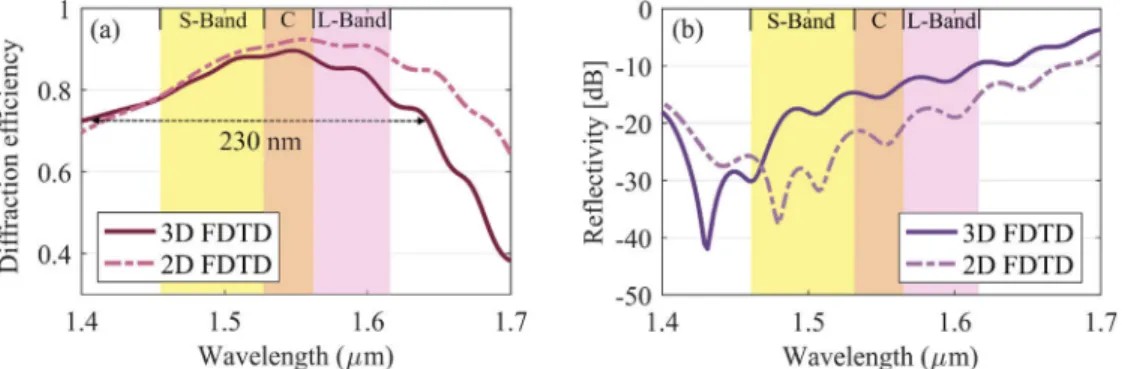
Using 10 periods for the antenna gratings, we found the following optimized values for the structural parameters: X= [289 nm, 217 nm, 209 nm, 283 nm, 272 nm, 210 nm, 2.64, 2.39]. As the next step, we performed wavelength scans for this optimized structure. Figure3(a) shows the diffraction efficiency for a wavelength range from 1.4 µm to 1.7 µm. First, we performed 2D FDTD simulation (Fig.3, dashed curves). A broad 1-dB bandwidth of 230 nm is achieved near the central wavelength of 1.55 µm. It is also observed that the S, C and L optical communication bands all fit within the 1-dB bandwidth of our antenna. In Fig.3(b) we show the grating modal reflectivity, i.e. the fraction of back-reflected power that couples into the counter propagating TE mode of the input waveguide. A reflectivity of less than -13 dB is predicted over the S, C and L optical communication bands.
Fig. 3. 2D and 3D FDTD simulation results for the (a) upward diffraction efficiency and (b) back-reflection, as a function of wavelength.
The SWG sections are periodically structured assuming a full etch with a pitch ΛSWG1,
ΛSWG2= 400 nm and duty cycle of DCSWG1= 0.7 for the SWG in the first (apodized) period and
the compatibility with deep UV lithography [22,23]. The total grating length (x-direction) is 7.6 µm. First, we used 3D FDTD simulations to evaluate the diffraction efficiency as a function of the antenna width for the optimized design with 10 periods without re-optimizing the structure for each width. As shown in Fig.4, in the transverse direction (along y-axis), an antenna width of 4.5 µm guarantees a good trade-off between compactness and efficiency penalty.
Fig. 4. Diffraction efficiency at λ=1550 nm for optimized antenna with 10 grating periods, as a function of waveguide width.
Rigorous 3D FDTD simulations were also used to validate the spectral behavior of the antenna and results are reported on Fig.3(solid curves) that confirms a good agreement with 2D analysis. The efficiency at λ= 1550 nm obtained from 2D and 3D simulations is 0.92 and 0.89, respectively, while the reflectivity is -23 dB (2D) and -15.5 dB (3D). Reflectivity remains below -10 dB over the S, C and L optical communication bands. The ripples that appear in diffraction efficiency and reflection spectra are due to the abrupt transition at the end of the grating. An additional grating period acting as an anti-reflective layer could be inserted at the end of the grating to reduce reflection and mitigate the resulting interference pattern.
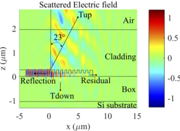
Figure5shows the simulated electric field distribution (the real part of Ey). Less than 5%
of the power is diffracted downwards and the residual power in the waveguide at the end of the grating is about 3%.
Fig. 5. 3D FDTD simulation of electric field distribution of the optimized antenna. The real part of Eyis shown. Silicon substrate is also included in the simulation window.
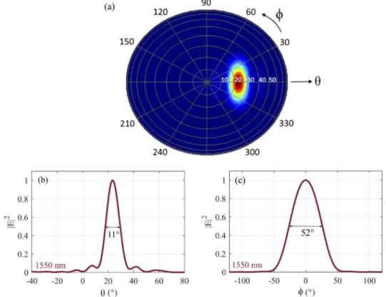
The far field radiation pattern of the antenna as a function of θ (polar angle) and ϕ (azimuthal angle) is shown in Fig.6. The diffraction angle is 23° from the vertical and the full width at half maximum (FWHM) of far-field intensity along the polar and azimuth coordinate is 11° and 52° at 1550 nm, respectively. The radiation angle wavelength shift is 0.12°/nm, over 1.5 µm - 1.6 µm wavelength range with a variation of the diffraction efficiency of about 4% over the same range.
Fig. 6. a) Antenna far-field radiation pattern at 1550 nm wavelength. b) Far-field distribution as a function of θ (for ϕ= 0) and c) along φ (for θ = 23°). (Far-field intensity distribution is normalized to the maximum far-field intensity).
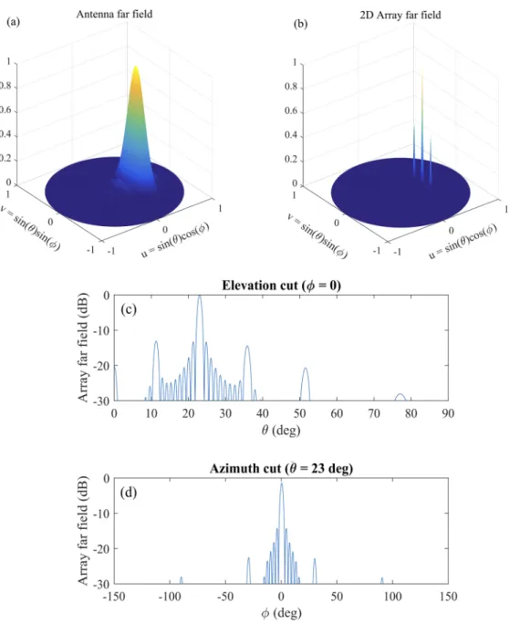
In our study we focus on the fundamental characteristics of the building block antenna component, such as the directional emission efficiency, broadband operation and small footprint. These antennas can be applied to many applications, including broadband fiber-chip couplers and optical phased arrays (OPAs). In particular, for the OPA application, the small footprint of our antenna makes it possible to build a high-density large aperture array, which can benefit from the high directionality of the antennas for increased efficiency. It is also important to minimize the separation between the array elements, for maximizing the steering range with a high radiation efficiency. In order to evaluate the performance of our antenna in a 2D array, we simulated a 10×10 array of gratings placed on a rectangular grid with a spacing of 8 µm in both the x and y directions. The far field of the array is calculated as the product of the antenna far field and the array factor function. The simulated far fields of the antenna and of the array are shown in Fig.7(a) and Fig.7(b), respectively, while the far field elevation cut (ϕ= 0) is shown in Fig.7(c), and Fig.7(d) shows the azimuthal cut (θ= 23°). It is observed that the grating lobes are separated by 11.2°, as expected from the array spacing of 8 µm. The calculated lobe-free steering range is θ × ϕ= 11.2° × 90°, which compares favorably with the state-of-the-art devices [52]. Furthermore, at the peak radiation angle of the array (θ= 23°), the efficiency is 89%. This is among the highest design efficiency reported for an antenna array in silicon waveguides.
Fig. 7. Calculated far field of a) the single grating antenna, b) the 10×10 array of gratings with an 8 µm spacing in both x and y directions, the array far field c) elevation cut at ϕ= 0°, and d) azimuthal cut at θ= 23°.
The design parameters for the antenna certainly differ for different applications. While for the fiber-chip couplers the grating antenna should match the size of the fiber aperture for efficient light coupling between the chip and the fiber, in the OPA applications the antenna size should be as small as possible to maximize the steering range [4]. The fiber-chip couplers are limited in bandwidth mainly because of the diffraction angle dependence with the wavelength which significantly impact the fiber coupling efficiency, with the fiber-chip diffraction angles typically in the range from 0° to 25° [1,12,13]. On the other hand, in the OPA applications, the angular width of diffracted field of the single antenna limits the maximum scanning range of the array.
4. Fabrication tolerance analysis
An important aspect of our antenna design is the evaluation of the tolerance to fabrication errors. To investigate fabrication tolerances, we considered variations of structural parameters for three possible fabrication errors. We consider the effect of structural size variations in both the propagation and transverse directions. The first source of uncertainty is a possible mask misalignment between the shallow and deep etch patterns. In this case, the misalignment produces errors only in the direction of propagation. Figure8(a) shows the schematic view of mask misalignment of δ < 0 resulting in an extra un-etched section of length δ between the shallow etch part of the L-shape and SWG segments as well as dimensional changes of L′3,6= L3,6
+ δ. Mask misalignment δ > 0 (Fig.8(b)) results in the SWG segments being partially etched. To simulate this case, an additional shallow-etched section of length δ having the same SWG duty cycle and pitch of section L1and L4is placed between the shallow etch part of the L-shape
and SWG segments, yielding L′3,6= L3,6+ δ and L′1,2,4,5= L1,2,4,5–δ.
Another important fabrication error can arise from the dimensional errors in the fully etched features of the antenna, i.e. the holes in the SWG regions (Fig.8(c)). To investigate the influence of this error, first we assume the effect of under-etching δ < 0, that is the SWG holes being smaller than the nominal value. In this case, L´
1,4= L1,4+ δ and two un-etched sections are added
having identical lengths of δ/2 between each side of SWG section, reducing the hole size along the x-direction. In y-direction, the etched and un-etched parts of SWG sections are modified as: w′1,3= w1,3+ δ, w′2,4= w2,4+ δ. To simulate the effect of over–etching (SWG holes larger than
the nominal value), two δ/2 length sections are added between each side of SWG region, while for the SWG region in proximity to the partial etched lengths of L-shape (L2, L5) it becomes
partially etched (Fig.8(d)). In this case δ > 0, the structural parameters are: L2,3,5,6′ = L2,3,5,6−δ/2
w′1,3= w1,3+ δ
w′2,4= w2,4−δ.
(2)
Finally, we study the effect of dimensional deviations of the shallow etched regions. For over etching δ > 0, L´2,5= L2,5+ δ/2, L´1,3,4,6= L1,3,4,6−δ/2, i.e. shallow-etched section of length δ/2
is added to represent the over-etched part on the length of the shallow etch regions (Fig.8(e)). In Fig.8(f), similarly, the under-etching δ < 0 is estimated by adding a section with length of δ/2 between etch L-shape and SWG segments, yielding:
L2′= L2+ δ
L′3,6= L3,6−δ/2
L′5= L5+ δ/2.
(3)
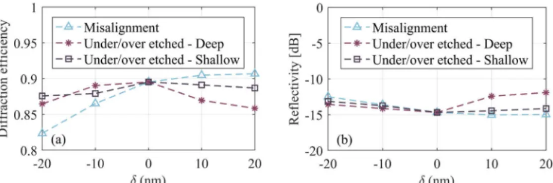
Figure9shows the upward diffraction efficiency and back reflections computed with 3D FDTD for different types of fabrication errors, considering dimensional variations (δ) between ±20 nm.
Fig. 8. Schematic top view of structural size variations for the first cell of the structure; a) and b) mask misalignment; c) and d) under/over full etch, e) and f) under/over shallow etch.
As can be seen, the changes in diffraction efficiency are more pronounced over the ±20 nm range for the case of mask misalignment error, which is expected since this misalignment affects the dimensional aspect ratio between L-shape and SWG sections. The back reflection variations remain comparatively small for these fabrication errors (Fig.9(b)).
Fig. 9. a) Diffraction efficiency and b) back reflections for three different types of fabrication errors.
Finally, we also considered the impact that a variation of the core thickness could have on the grating performance. This variability is expected to be much smaller than the fabrication variations related to the lithography considered above, with standard deviation on the order of 1 nm [53]. Assuming a silicon thickness of 300 ± 5 nm, while keeping the other grating dimensions unchanged, we obtained a negligible variation of <1% for both diffraction efficiency and reflection, compared to the nominal case.
5. Conclusions
In this paper, we proposed a new type of silicon grating antenna based on SWG metamaterials on a 300-nm SOI platform, simultaneously achieving high diffraction efficiency and directionality, and broadband operation, with a compact device footprint. Our 3D FDTD simulations predict a peak diffraction efficiency of 0.89 (-0.5 dB) with a 1-dB bandwidth of 230 nm. Back-reflections as low as -15 dB are achieved. The compact antenna (7.6 µm × 4.5 µm) has a minimum feature size of 120 nm, which is compatible with UV lithography, with a robust tolerance to common nanofabrication errors. By leveraging subwavelength metamaterial engineering, this novel compact and highly efficient nanoantenna design opens a promising path towards development of a new library of integrated photonic components for applications in optical phased arrays and off-chip interconnects.
Funding.National Research Council Canada ((HTSN 604), (CSTIP), (HTSN 209), New Ideation Program, Technology and Innovation Program); Canada Research Chairs; Natural Sciences and Engineering Research Council of Canada.
Acknowledgements.The authors acknowledge Lei Yuan for assisting with the optical phased array simulations.
Disclosures.The authors declare no conflicts of interest.
References
1. D. Melati, M. Kamandar Dezfouli, Y. Grinberg, J. H. Schmid, R. Cheriton, S. Janz, P. Cheben, and D. X. Xu, “Design of compact and efficient silicon photonic micro antennas with perfectly vertical emission,”IEEE J. Sel. Top. Quantum Electron.27(1), 1–10 (2021).
2. T. Kim, P. Bhargava, C. V. Poulton, J. Notaros, A. Yaacobi, E. Timurdogan, C. Baiocco, N. Fahrenkopf, S. Kruger, T. Ngai, Y. Timalsina, M. R. Watts, and V. Stojanovic, “A single-chip optical phased array in a wafer-scale silicon photonics/CMOS 3D-integration platform,”IEEE J. Solid-State Circuits54(11), 3061–3074 (2019).
3. J. L. Pita, I. Aldaya, P. Dainese, H. E. Hernandez-Figueroa, and L. H. Gabrielli, “Design of a compact CMOS-compatible photonic antenna by topological optimization,”Opt. Express26(3), 2435–2442 (2018).
4. J. Sun, E. Timurdogan, A. Yaacobi, E. S. Hosseini, and M. R. Watts, “Large-scale nanophotonic phased array,”
Nature493(7431), 195–199 (2013).
5. R. Fatemi, A. Khachaturian, and A. Hajimiri, “A nonuniform sparse 2-D large-FOV optical phased array with a low-power PWM drive,”IEEE J. Solid-State Circuits54(5), 1200–1215 (2019).
6. H. Abediasl and H. Hashemi, “Monolithic optical phased-array transceiver in a standard SOI CMOS process,”Opt. Express23(5), 6509–6519 (2015).
7. L. Novotny, Optical Antennas: A New Technology That Can Enhance Light-Matter Interactions (Frontiers of Engineering, 2012).
8. D. Vermeulen, S. Selvaraja, P. Verheyen, G. Lepage, W. Bogaerts, P. Absil, D. Van Thourhout, and G. Roelkens, “High-efficiency fiber-to-chip grating couplers realized using an advanced CMOS-compatible Silicon-On-Insulator platform,”Opt. Express18(17), 18278–18283 (2010).
9. D. Melati, Y. Grinberg, M. Kamandar Dezfouli, S. Janz, P. Cheben, J. H. Schmid, A. Sánchez-Postigo, and D. X. Xu, “Mapping the global design space of nanophotonic components using machine learning pattern recognition,”Nat. Commun.10(1), 1–9 (2019).
10. T. Watanabe, M. Ayata, U. Koch, Y. Fedoryshyn, and J. Leuthold, “Perpendicular grating coupler based on a blazed antiback-reflection structure,”J. Lightwave Technol.35(21), 4663–4669 (2017).
11. D. Benedikovic, C. Alonso-Ramos, P. Cheben, J. H. Schmid, S. Wang, D.-X. Xu, J. Lapointe, S. Janz, R. Halir, A. Ortega-Moñux, J. G. Wangüemert-Pérez, I. Molina-Fernández, J.-M. Fédéli, L. Vivien, and M. Dado, “High-directionality fiber-chip grating coupler with interleaved trenches and subwavelength index-matching structure,”Opt. Lett.40(18), 4190–4193 (2015).
12. C. Alonso-Ramos, P. Cheben, A. Ortega-Moñux, J. H. Schmid, D.-X. Xu, and I. Molina-Fernández, “Fiber-chip grating coupler based on interleaved trenches with directionality exceeding 95%,”Opt. Lett.39(18), 5351–5354
(2014).
13. D. Benedikovic, C. Alonso-Ramos, S. Guerber, X. Le Roux, P. Cheben, C. Dupré, B. Szelag, D. Fowler, É. Cassan, D. Marris-Morini, C. Baudot, F. Boeuf, and L. Vivien, “Sub-decibel silicon grating couplers based on L-shaped waveguides and engineered subwavelength metamaterials,”Opt. Express27(18), 26239–26250 (2019).
14. M. Passoni, D. Gerace, L. Carroll, and L. C. Andreani, “Grating couplers in silicon-on-insulator: The role of photonic guided resonances on lineshape and bandwidth,”Appl. Phys. Lett.110(4), 41107–41111 (2017).
15. D. Benedikovic, P. Cheben, J. H. Schmid, D. Xu, J. Lapointe, S. Wang, R. Halir, A. Ortega-Moñux, S. Janz, and M. Dado, “High-efficiency single etch step apodized surface grating coupler using subwavelength structure,”Laser Photonics Rev.8(6), L93–L97 (2014).
16. D. Taillaert, P. Bienstman, and R. Baets, “Compact efficient broadband grating coupler for silicon-on-insulator waveguides,”Opt. Lett.29(23), 2749–2751 (2004).
17. W. Zhou, Z. Cheng, X. Chen, K. Xu, X. Sun, and H. Tsang, “Subwavelength engineering in silicon photonic devices,”
IEEE J. Sel. Top. Quantum Electron.25(3), 1–13 (2019).
18. D. Benedikovic, C. Alonso-Ramos, D. Pérez-Galacho, S. Guerber, V. Vakarin, G. Marcaud, X. Le Roux, E. Cassan, D. Marris-Morini, P. Cheben, F. Boeuf, C. Baudot, and L. Vivien, “L-shaped fiber-chip grating couplers with high directionality and low reflectivity fabricated with deep-UV lithography,”Opt. Lett.42(17), 3439–3442 (2017).
19. M. Kamandar Dezfouli, Y. Grinberg, D. Melati, P. Cheben, J. Schmid, A. Sánchez-Postigo, A. Ortega-Moñux, J. G. Wangüemert-Pérez, R. Cheriton, S. Janz, and D.-X. Xu, “Perfectly vertical surface grating couplers using subwavelength engineering for increased feature sizes,”Opt. Lett.45(13), 3701–3704 (2020).
20. R. Halir, A. Ortega-Moñux, D. Benedikovic, G. Z. Mashanovich, J. G. Wangüemert-Pérez, J. H. Schmid, Í. Molina-Fernández, and P. Cheben, “Subwavelength-grating metamaterial structures for silicon photonic devices,”Proc. IEEE
106(12), 2144–2157 (2018).
21. R. Halir, P. Cheben, J. H. Schmid, R. Ma, D. Bedard, S. Janz, D.-X. Xu, A. Densmore, J. Lapointe, and Í. Molina-Fernández, “Continuously apodized fiber-to-chip surface grating coupler with refractive index engineered subwavelength structure,”Opt. Lett.35(19), 3243–3245 (2010).
22. J. H. Schmid, P. Cheben, P. J. Bock, R. Halir, J. Lapointe, S. Janz, A. Delage, A. Densmore, J.-M. Fedeli, T. J. Hall, B. Lamontagne, R. Ma, I. Molina-Fernandez, and D.-X. Xu, “Refractive Index Engineering With Subwavelength Gratings in Silicon Microphotonic Waveguides,”IEEE Photonics J.3(3), 597–607 (2011).
23. J. D. Sarmiento-Merenguel, A. Ortega-Moñux, J.-M. Fédéli, J. G. Wangüemert-Pérez, C. Alonso-Ramos, E. Durán-Valdeiglesias, P. Cheben, Í. Molina-Fernández, and R. Halir, “Controlling leakage losses in subwavelength grating silicon metamaterial waveguides,”Opt. Lett.41(15), 3443–3446 (2016).
24. D. X. Xu, J. H. Schmid, G. T. Reed, G. Z. Mashanovich, D. J. Thomson, M. Nedeljkovic, X. Chen, D. Van Thourhout, S. Keyvaninia, and S. K. Selvaraja, “Silicon photonic integration platform-Have we found the sweet spot?”IEEE J. Sel. Top. Quantum Electron.20(4), 189–205 (2014).
25. A. Bozzola, L. Carroll, D. Gerace, I. Cristiani, and L. C. Andreani, “Optimising apodized grating couplers in a pure SOI platform to −0.5 dB coupling efficiency,”Opt. Express23(12), 16289–16304 (2015).
26. S. Khajavi, D. Melati, P. Cheben, J. H. Schmid, D.-X. Xu, S. Janz, and W. N Ye, “Design of compact silicon antennas based on high directionality gratings,” in IEEE Photonics Conference (IPC, 2020), pp. 1–2.
27. H. Y. Chen and K. C. Yang, “Design of a high-efficiency grating coupler based on a silicon nitride overlay for silicon-on-insulator waveguides,”Appl. Opt.49(33), 6455–6462 (2010).
28. S. Yang, Y. Zhang, T. Baehr-Jones, and M. Hochberg, “High efficiency germanium-assisted grating coupler,”Opt. Express22(25), 30607–30612 (2014).
29. J. H. Schmid, P. Cheben, S. Janz, J. Lapointe, E. Post, and D.-X. Xu, “Gradient-index antireflective subwavelength structures for planar waveguide facets,”Opt. Lett.32(13), 1794–1796 (2007).
30. P. Cheben, D.-X. Xu, S. Janz, and A. Densmore, “Subwavelength waveguide grating for mode conversion and light coupling in integrated optics,”Opt. Express14(11), 4695–4702 (2006).
31. J. H. Schmid, P. Cheben, S. Janz, J. Lapointe, E. Post, A. Delâge, A. Densmore, B. Lamontagne, P. Waldron, and D.-X. Xu, “Subwavelength grating structures in planar waveguide facets for modified reflectivity,”Proc. SPIE6796,
67963E1–67963E10 (2007).
32. P. J. Bock, P. Cheben, J. H. Schmid, A. Delâge, D.-X. Xu, S. Janz, and T. J. Hall, “Sub-wavelength grating mode transformers in silicon slab waveguides,”Opt. Express17(21), 19120–19133 (2009).
33. P. Cheben, J. H. Schmid, D.-X. Xu, A. Densmore, and S. Janz, “Composite subwavelength-structured waveguide in optical systems,” U.S. patent 8,503,839B2 (August 6, 2013).
34. P. Cheben, R. Halir, J. H. Schmid, H. A. Atwater, and D. R. Smith, “Subwavelength integrated photonics,”Nature
560(7720), 565–572 (2018).
35. P. Cheben, S. Janz, D. X. Xu, B. Lamontagne, A. Delâge, and S. Tanev, “A broad-band waveguide grating coupler with a subwavelength grating mirror,”IEEE Photonics Technol. Lett.18(1), 13–15 (2006).
36. Q. Zhong, V. Veerasubramanian, Y. Wang, W. Shi, D. Patel, S. Ghosh, A. Samani, L. Chrostowski, R. Bojko, and D. V. Plant, “Focusing-curved subwavelength grating couplers for ultra-broadband silicon photonics optical interfaces,”
Opt. Express22(15), 18224–18231 (2014).
37. A. Sánchez-Postigo, J. Gonzalo Wangüemert-Pérez, J. M. Luque-González, Í. Molina-Fernández, P. Cheben, C. A. Alonso-Ramos, R. Halir, J. H. Schmid, and A. Ortega-Moñux, “Broadband fiber-chip zero-order surface grating coupler with 0.4 dB efficiency,”Opt. Lett.41(13), 3013–3016 (2016).
38. Y. Wang, W. Shi, X. Wang, Z. Lu, M. Caverley, R. Bojko, L. Chrostowski, and N. A. F. Jaeger, “Design of broadband subwavelength grating couplers with low back reflection,”Opt. Lett.40(20), 4647–4650 (2015).
39. J. Zou, Y. Yu, and X. Zhang, “Single step etched two dimensional grating coupler based on the SOI platform,”Opt. Express23(25), 32490–32495 (2015).
40. J. Zou, Y. Yu, and X. Zhang, “Two-dimensional grating coupler with a low polarization dependent loss of 0.25 dB covering the C-band,”Opt. Lett.41(18), 4206–4209 (2016).
41. J. Kang, Z. Cheng, W. Zhou, T.-H. Xiao, K.-L. Gopalakrisna, M. Takenaka, H. K. Tsang, and K. Goda, “Focusing subwavelength grating coupler for mid-infrared suspended membrane germanium waveguides,”Opt. Lett.42(11),
2094–2097 (2017).
42. Y. Wang, X. Wang, J. Flueckiger, H. Yun, W. Shi, R. Bojko, N. A. F. Jaeger, and L. Chrostowski, “Focusing sub-wavelength grating couplers with low back reflections for rapid prototyping of silicon photonic circuits,”Opt. Express22(17), 20652–20662 (2014).
43. X. Chen and H. K. Tsang, “Nanoholes grating couplers for coupling between silicon-on-insulator waveguides and optical fibers,”IEEE Photonics J.1(3), 184–190 (2009).
44. X. Xu, H. Subbaraman, D. Kwong, J. Covey, A. Hosseini, and R. T. Chen, “Colorless grating couplers realized by interleaving dispersion engineered subwavelength structures,” in Conference on Lasers and Electro-Optics (CLEO, 2013), pp. 3588–3591.
45. L. Carroll, D. Gerace, I. Cristiani, and L. C. Andreani, “Optimizing polarization-diversity couplers for Si-photonics: reaching the −1 dB coupling efficiency threshold,”Opt. Express22(12), 14769–14781 (2014).
46. D. Benedikovic, C. Alonso-Ramos, P. Cheben, J. H. Schmid, S. Wang, R. Halir, A. Ortega-Moñux, D.-X. Xu, L. Vivien, J. Lapointe, S. Janz, and M. Dado, “Single-etch subwavelength engineered fiber-chip grating couplers for 13 µm datacom wavelength band,”Opt. Express24(12), 12893–12904 (2016).
47. X. Chen, D. J. Thomson, L. Crudginton, A. Z. Khokhar, and G. T. Reed, “Dual-etch apodised grating couplers for efficient fibre-chip coupling near 1310 nm wavelength,”Opt. Express25(15), 17864–17871 (2017).
48. Y. Tong, W. Zhou, and H. Ki Tsang, “Efficient perfectly vertical grating coupler for multi-core fibers fabricated with 193 nm DUV lithography,”Opt. Lett.43(23), 5709–5712 (2018).
49. C. R. Houck, J. Joines, and M. G. Kay, “A genetic algorithm for function optimization: a Matlab implementation,”
Ncsu-ie tr95(09), 1–10 (1995).
50. P. J. Bock, P. Cheben, J. H. Schmid, J. Lapointe, A. Delâge, S. Janz, G. C. Aers, D.-X. Xu, A. Densmore, and T. J. Hall, “Subwavelength grating periodic structures in silicon-on-insulator: a new type of microphotonic waveguide,”
Opt. Express18(19), 20251–20262 (2010).
51. P. Cheben, J. H. Schmid, R. Halir, A. Sánchez-Postigo, D. X. Xu, S. Janz, J. Lapointe, S. Wang, M. Vachon, A. Ortega-Moñux, G. Wangüemert-Pérez, I. Molina-Fernández, J. M. Luque-Gonzalez, J. D. Sarmiento-Merenguel, J. Pond, D. Benedikovic, C. Alonso-Ramos, M. Dado, J. Müllerová, M. Pánes, and V. Vasinek, “Subwavelength index engineered waveguides and devices,” in Optical Fiber Communication Conference (OFC, 2017), paper Tu3K-2. 52. M. J. R. Heck, “Highly integrated optical phased arrays: Photonic integrated circuits for optical beam shaping and
beam steering,”Nanophotonics6(1), 93–107 (2017).
53. Y. Xing, M. Wang, A. Ruocco, J. Geessels, U. Khan, and W. Bogaerts, “Compact silicon photonics circuit to extract multiple parameters for process control monitoring,”OSA Continuum3(2), 379–390 (2020).
![Fig. 1. (a) Three dimensional (3D) schematics of the antenna. (b) Two dimensional (2D) longitudinal cross-section of the structure with grating periods Λ 1 and Λ 2 and structural parameters [L 1 , L 2 , L 3 , L 4 , L 5 , L 6 , n SWG1 , n SWG2 ]](https://thumb-eu.123doks.com/thumbv2/123doknet/13969345.453612/4.918.203.712.143.502/dimensional-schematics-antenna-dimensional-longitudinal-structure-structural-parameters.webp)