HAL Id: hal-01742002
https://hal.archives-ouvertes.fr/hal-01742002
Submitted on 27 Mar 2018
HAL is a multi-disciplinary open access
archive for the deposit and dissemination of
sci-entific research documents, whether they are
pub-lished or not. The documents may come from
teaching and research institutions in France or
abroad, or from public or private research centers.
L’archive ouverte pluridisciplinaire HAL, est
destinée au dépôt et à la diffusion de documents
scientifiques de niveau recherche, publiés ou non,
émanant des établissements d’enseignement et de
recherche français ou étrangers, des laboratoires
publics ou privés.
Lateral epitaxial growth of germanium on silicon oxide
D. Cammilleri, V. Yam, F. Fossard, C. Renard, D. Bouchier, Pier-Francesco
Fazzini, Luca Ortolani, Florent Houdellier, Martin Hÿtch
To cite this version:
D. Cammilleri, V. Yam, F. Fossard, C. Renard, D. Bouchier, et al.. Lateral epitaxial growth of
germanium on silicon oxide. Applied Physics Letters, American Institute of Physics, 2008, 93 (4),
pp.43110 - 43110. �10.1063/1.2963363�. �hal-01742002�
Lateral epitaxial growth of germanium on silicon oxide
V. D. Cammilleri, V. Yam, F. Fossard, C. Renard, D. Bouchier, P. F. Fazzini, L. Ortolani, F. Houdellier, and M. Hÿtch
Citation: Appl. Phys. Lett. 93, 043110 (2008); doi: 10.1063/1.2963363 View online: https://doi.org/10.1063/1.2963363
View Table of Contents: http://aip.scitation.org/toc/apl/93/4
Published by the American Institute of Physics
Articles you may be interested in
High hole mobility tin-doped polycrystalline germanium layers formed on insulating substrates by low-temperature solid-phase crystallization
Applied Physics Letters 107, 022103 (2015); 10.1063/1.4926507
Selective growth of Ge on Si(100) through vias of nanotemplate using solid source molecular beam epitaxy
Applied Physics Letters 83, 5032 (2003); 10.1063/1.1632037
Origin and removal of stacking faults in Ge islands nucleated on Si within nanoscale openings in SiO2
Journal of Applied Physics 110, 073516 (2011); 10.1063/1.3643003
Defects reduction of Ge epitaxial film in a germanium-on-insulator wafer by annealing in oxygen ambient
APL Materials 3, 016102 (2015); 10.1063/1.4905487
High quality relaxed germanium layers grown on (110) and (111) silicon substrates with reduced stacking fault formation
Journal of Applied Physics 114, 154306 (2013); 10.1063/1.4825130
Electrical properties of pseudo-single-crystalline germanium thin-film-transistors fabricated on glass substrates
Lateral epitaxial growth of germanium on silicon oxide
V. D. Cammilleri,1 V. Yam,1,a兲 F. Fossard,1 C. Renard,1 D. Bouchier,1 P. F. Fazzini,2 L. Ortolani,2,3F. Houdellier,2and M. Hÿtch2
1
Institut d’Electronique Fondamentale, CNRS UMR 8622, Université Paris-Sud, Bât 220, 91405 Orsay, France
2
CEMES-CNRS, University of Toulouse, 29, Rue Jeanne Marvig, 31055, Toulouse Cedex 4, France
3
University of Bologna, Department of Physics, v.le B. Pichat, 6/2, 40127 Bologna, Italy and CNR-IMM Bologna, v. Gobetti, 101, 40129 Bologna, Italy
共Received 20 May 2008; accepted 3 July 2008; published online 29 July 2008兲
We have developed a method using local oxidation on silicon to create nanoscale silicon seeds for the lateral epitaxial overgrowth of germanium on silicon oxide. The germanium growth starts selectively from silicon seed lines, proceeds by wetting the SiO2 layer and coalesces without
formation of grain boundary. Analysis by high resolution transmission electron microscopy have shown that Ge layers grown above silicon oxide are perfectly monocrystalline and are free of defect. The only detected defects are situated at the Ge/Si interface. Geometrical phase analyses of the microscopy images have shown that the Ge layer is fully relaxed and homogeneous. © 2008 American Institute of Physics. 关DOI:10.1063/1.2963363兴
Germanium used as a high mobility channel, presents a strong interest for fully depleted metal oxide semiconductor field effect transistors to be developed in the next comple-mentary metal oxide semiconductor technology generation 共22 nm and below兲.1
Currently germanium on insulator-共GeOI兲 structures are fabricated in the form of plain wafers by bonding techniques such as etch back or SMARTCUT,2 or by Ge condensation.3 In this paper, we propose the lateral epitaxial growth 共LEG兲 of germanium on a SiO2 layer
formed by oxidation of a standard silicon wafer as an alter-native to these techniques.4 Such a local approach have the advantage of enabling easily the manufacturing of Ge- and Si-based devices at the same level on the wafer, and, from the material point of view, can be effective for defect density reduction, thanks to the low dimensions of the LEG crystals.5 It is well known that the main difficulty for growing germanium on silicon stems from a mismatch of 4.2% be-tween the two crystal lattices, what results, on plain wafers, in the emission of misfit dislocations as soon as the growing film exceeds a critical thickness standing in the order of 1 nm.6 When starting from seeds of limited diameter, a growing mismatched crystal is free of accommodating its lattice in a three-dimensional volume, which opens the pos-sibility of dislocation-free growth. Previous calculations7 have shown that for a given mismatch, the critical film thick-ness strongly depends on the seed radius and tends to the infinite below a critical radius value, which would be close to 20 nm for a mismatch of 4.2%. The validity of this approach has been demonstrated with the growth of dislocation-free Ge on silicon covered with a very thin SiO2film.8,9
We have developed a method to create nanoscale silicon seeds for lateral epitaxial of Ge on silicon oxide by using local oxidation of silicon 共LOCOS兲 within a silicon nitride pattern mask. To realize the LOCOS, a silicon nitride film 共⬃50 nm thick兲 is deposited on p-type Si共001兲 substrates by plasma enhanced chemical vapor deposition 共PECVD兲 and patterned by conventional deep UV lithography 共248 nm兲
and reactive ion etching. Silicon nitride patterns consisting of 0.3– 10m wide lines oriented along the具110典 direction are made. A wet oxidation at 1050 ° C is then performed in order to grow a ⬃100 nm thick silicon oxide layer through the nitride mask. At this oxidation temperature, flat 兵111其 inter-faces between silicon oxide and Si are formed close to the bird’s beaks, as shown in Ref. 10. The oxide layer is then partially etched using a hydrofluoric 共HF兲 acid solution to partially free the 兵111其 facets from SiO2, in order to create
lateral nucleation seeds for the Ge growth. The growth of Ge on Si surface close to the 共111兲 orientation is of special in-terest, since in this orientation the misfit dislocations can glide along共111兲 planes.11It is worth noting that the width of the seeds and the thickness of the SiO2 layer can be easily and precisely adjusted by controlling the thermal oxidation time and the etching time in HF solution. Figure1共a兲shows a cross sectional scanning electron microscopy共SEM兲 image of a linear silicon seed formed between Si3N4and SiO2. The
width of the seed line is inferior to 50 nm. The SiO2 layer
thickness is around 50 nm, and as expected, the surface ori-entation of the Si seed is close to 共111兲.
The epitaxial growth of Ge on the so formed patterns is carried out in an ultrahigh vacuum chemical vapor deposi-tion 共UHV CVD兲 reactor with a base pressure of 2 ⫻10−10Torr using germane共GeH
4兲 diluted at 10% in H2. As
growth of Ge from GeH4 is naturally selective on Si versus
silicon oxide, the growth conditions are chosen to avoid polycrystalline Ge deposition on the nitride mask. The growth temperature is set up at 600 ° C under a total pressure of 1⫻10−2Torr, while the growth time varies between 1 and
2 h.
The growth process is monitored in situ by reflection high energy electron diffraction共RHEED兲. The RHEED dia-grams recorded during growth show only spotty and streaky patterns, no polycrystalline signature共rings兲 being detected, which indicates clearly a monocrystalline growth. Figure 1
shows cross sectional SEM images illustrating different stages of Ge lateral growth from the Si seeds. The Ge growth is selective, it starts from the Si seeds, as shown on Fig.1共b兲, and proceeds laterally by “wetting” the SiO2layer following
a兲Author to whom correspondence should be addressed. Electronic mail:
vy.yam@u-psud.fr.
APPLIED PHYSICS LETTERS 93, 043110共2008兲
an angle close to 125°. This angle corresponds to 兵11−1其 facet, while the LEG Ge crystals exhibit 兵113其 and 兵111其 facets in their upper part关Fig.1共c兲兴. Coalescence of Ge crys-tals from adjacent seeds takes place for longer deposition time and leads to rooflike structures delimited by 兵113其 and 兵111其 facets 关Fig. 1共d兲兴, as currently observed for selective
epitaxial growth of Ge layers.12The orientation of the seed patterns appears to be an essential parameter. The Ge crystals grows straight and parallel to the seed lines when these latter are oriented along the具110典 direction, as seen in Fig.1共b兲. In the具110典 orientation, stable Ge facets can be formed.13When seed lines are disoriented with respect to the具110典 direction, the Ge growth is more irregular, facet formation becomes unfavorable for lateral growth. This results in the formation of separated faceted crystals along the seeds, as shown in Fig.2.
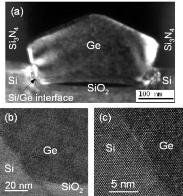
To better study the Ge structures, transmission electron microscopy共TEM兲 analysis is carried out on cross sectional specimens in a Cs-corrected Tecnai F20 installed at CEMES-CNRS. As a first step, weak beam dark field analysis14 共WBDF兲 is used to investigate the presence of extended de-fects in the Ge crystals. Figure 3共a兲is a WBDF image of a coalesced germanium crystal taken in a g = 220, 共g,−2g兲
condition. No defect is visible in the inner part of the struc-ture while the contrast zones found at the two Si/Ge inter-faces confirm the presence of defects due to the misfit be-tween bulk silicon and germanium. Moreover several plane view TEM analysis show that the joining of two front s result in defect-free interface. This means that the Ge crystals have evolved from a growth shape to an equilibrium shape during the coalescence, with a reorganization of the material that leads to a new grain-boundary-free Ge crystal.
These results are compatible with the hypothesis that LEG Ge consists in fully relaxed single crystals free of bulk defects. High Resolution TEM analysis 共HRTEM兲 is carried out on the same specimen关Figs.3共b兲and3共c兲兴. The recorded images confirm that as grown Ge is fully crystalline. In ad-dition, HRTEM images obtained in the Si/Ge interface re-gion关Fig.3共c兲兴 indicate the presence of stacking fault s and FIG. 1. Cross sectional SEM images of a linear Si seed oriented along the具110典 direction 共a兲 and of Ge crystals grown from the Si seeds at different deposition times: 1 h共b兲, 1 h and 45 min 共c兲, and 2 h 共d兲.
FIG. 2. Ge crystals grown from linear seeds disoriented by 22° from the 具110典 direction.
FIG. 3. TEM WBDF images obtained in a g = 220,共g,−2 g兲 condition from a Ge crystal共a兲 and HREM images 关共b兲 and 共c兲兴 of the Ge/Si interface.
interfacial dislocations at the interface. The defect density appears to be very low at the Ge/Si interfaces. It is possible that the seed morphology 共roughness and orientation兲 helps plastic relaxation. The roughness confines dislocations at in-terface, and, the 共111兲 Ge/Si interface enables misfit dislo-cations to glide in the interfacial plane.11
In order to evaluate the amount of strain in germanium crystals, geometric phase analysis of HRTEM images is performed.15,16The lattice spacing is constant in the silicon layer far from the interface and it is used as the reference. As a consequence the measured strain is a relative value with respect to an unstrained silicon lattice. In Fig.4, the strain of the 共11−1兲 and 共200兲 planes are combined to determine the two-dimensional deformation tensor perpendicular to a具110典 zone axis. Two uniform zones of different constant strain are apparent in the image due to the change in the lattice spacing when passing from the silicon to the germanium region. It can be also observed, in Fig.4, that the expansion of the Ge lattice with respect to relaxed Silicon is uniform in the共110兲 and 共100兲 directions and amounts respectively to xx= + 3.8% andzz= + 4.2%. From these results we can conclude that the Ge crystal is almost fully relaxed, homogeneous and crystalline.
In conclusion, we have shown that large fully relaxed monocrystalline Ge crystals on SiO2 with very low defect
densities can be easily obtained by LEG. A reproducible method based on LOCOS has been developed to create well localized nanoscale apertures through the SiO2layer, that act as seeds for transferring the crystalline order from the Si substrate to the LEG Ge crystals. This local approach could be an attractive alternative to GeOI plain wafer for micro-and optoelectronic applications.
This work was supported by the Commission of Euro-pean Communities IP Pullnano 共IST contract No. 02828兲. The authors also thank the “Centrale de Technologie Univer-sitaire” MINERVE for the technological backup.
1F. Letertre, C. Deguet, C. Richtarch, B. Faure, J. M. Hartmann, F. Chieu,
A. Beaumont, J. Dechamp, C. Morales, F. Allibert, P. Perreau, S. Pocas, S. Personnic, C. Lagahe-Blanchard, B. Ghyselen, Y. M. Le Vaillant, E. Jalaguier, N. Kernevez, and C. Mazure, Proceedings of Symposium B of the MRS 2004 Spring Meeting, 12–16 April 2004, San Francisco, 2004 共unpublished兲.
2T. Akatsu, C. Deguet, L. Sanchez, F. Allibert, D. Rouchon, T.
Signama-rcheix, C. Richtarch, A. Boussagol, V. Loup, F. Mazen, J.-M. Hartmann, Y. Campidelli, L. Clavelier, F. Letertre, N. Kernevez, and C. Mazure, Materials Science in Semiconductor Processing 9, 444共2006兲.
3T. Tezuka, N. Sugiyama, and S. Takagi,Appl. Phys. Lett. 79, 1798共2001兲. 4D. Bouchier, V. Yam, D. Cammilleri, C. Renard, and F. Fossard, French
Patent No. FR 2007/59859共14 December 2007兲.
5F. R. N. Nabarro, Theory of Crystal Dislocations 共Oxford, New York,
1967兲.
6R. People and J. C. Bean,Appl. Phys. Lett. 47, 322共1985兲. 7S. Luryi and E. Suhir,Appl. Phys. Lett. 49, 140共1986兲.
8Q. Li, B. Pattada, S. R. J. Brueck, S. Hersee, and S. M. Han,J. Appl. Phys. 98, 073504共2005兲.
9M. Halbwax, C. Renard, D. Cammilleri, V. Yam, F. Fossard, D. Bouchier,
Y. Zheng, and E. Rzepka, J. Cryst. Growth 308, 26共2007兲.
10M. Okihara, S. Kuroda, M. Itoh, and N. Hirashita,Jpn. J. Appl. Phys., Part 1 34, 1822共1995兲.
11Th. Schmidt, R. Kröger, J. I. Flege, T. Clausen, J. Falta, A. Janzen, P. Zal,
P. Kury, M. Kammler, and H.-v. Hoegen, Phys. Rev. Lett. 96, 066101
共2006兲.
12M. Halbwax, L. H. Nguyen, F. Fossard, X. Le Roux, V. Mathet, V. Yam,
D. T. Cao, and D. Bouchier, Mater. Sci. Semicond. Process. 9, 460共2006兲.
13Z. Gai, W. S. Yang, R. G. Zhao, and T. Sakurai,Phys. Rev. B 59, 15230
共1999兲.
14D. B. Williams and C. B. Carter, Transmission Electron Microscopy A Textbook for Materials Science共Springer, New York, 2004兲.
15M. J. Hÿtch, E. Snoeck, and R. Kilaas,Ultramicroscopy 74, 131共1998兲. 16M. J. Hÿtch, J. L. Putaux, and J. M. Pénisson,Nature共London兲 423, 270
共2003兲. FIG. 4. 共Color online兲 Two-dimensional strain maps of the Germanium
seeds measured with reference to the silicon lattice. The strain value for relaxed germanium is=4.2%