HAL Id: hal-00795981
https://hal.archives-ouvertes.fr/hal-00795981
Submitted on 1 Mar 2013HAL is a multi-disciplinary open access archive for the deposit and dissemination of sci-entific research documents, whether they are pub-lished or not. The documents may come from teaching and research institutions in France or abroad, or from public or private research centers.
L’archive ouverte pluridisciplinaire HAL, est destinée au dépôt et à la diffusion de documents scientifiques de niveau recherche, publiés ou non, émanant des établissements d’enseignement et de recherche français ou étrangers, des laboratoires publics ou privés.
Validation of bending test by nanoindentation for
micro-contact analysis of MEMS switches
Adrien Broué, Thibeaut Fourcade, Jérémie Dhennin, Frédéric Courtade,
Pierre-Louis Charvet, Patrick Pons, X. Lafontan, Robert Plana
To cite this version:
Adrien Broué, Thibeaut Fourcade, Jérémie Dhennin, Frédéric Courtade, Pierre-Louis Charvet, et al.. Validation of bending test by nanoindentation for micro-contact analysis of MEMS switches. Journal of Micromechanics and Microengineering, IOP Publishing, 2010, 20 (6), pp.1-8. �hal-00795981�
Validation of bending test by nanoindentation for
micro-contact analysis of MEMS switches
Adrien Broue
1-2-3, Thibaut Fourcade
1-6, Jérémie Dhennin
1, Frédéric
Courtade
4, Pierre-Louis Charvet
5, Patrick Pons
2-3, Xavier Lafontan
7,
Robert Plana
2-31NovaMEMS ; c/o CNES 18 Avenue E. Belin 31401 Toulouse cedex 9, France 2CNRS ; LAAS ; 7 avenue du colonel Roche, F-31077 Toulouse, France
3Université de Toulouse ; UPS, INSA, INP, ISAE ; LAAS ; F-31077 Toulouse, France 4CNES ; 18 Avenue E. Belin 31401 Toulouse, France
5CEA-LETI, Minatec ; 17 rue des Martyrs, 38054 Grenoble Cedex 9, France 6LGP-ENIT, 47 Av. d'Azereix, BP 1629, 65016 Tarbes CEDEX, France 7INTESENS ; 10 Avenue de l’Europe 31520 Ramonville, France
adrien.broue@novamems.com
Abstract. Research on contact characterization for microelectromechanical system (MEMS)
switches has been driven by the necessity to reach a high-reliability level for micro-switch applications. One of the main failures observed during cycling of the devices is the increase of the electrical contact resistance. The key issue is the electromechanical behaviour of the materials used at the contact interface when the current is flowing through the contact asperities. Indeed metal contacting switches have a large and complex set of failure mechanisms driven by the current level. This paper demonstrates the validity of a new methodology using a commercial nanoindenter coupled with electrical measurements on test vehicles specially designed to investigate the micro-scale contact physics. Dedicated validation tests and modeling are performed to assess the introduced methodology by analysing the response of gold contact with 5 µm² square bumps under various levels of current flowing through contact asperities. Contact temperature rise is measured leading to shifts of the mechanical properties of contact material and modifications of the contact topology. In addition, the data provide a better understanding of micro-contact behaviour related to the impact of current at low- to medium-power levels.
Keywords. MEMS, reliability, micro-contact, contact temperature, nanoindenter, Au contact,
contact physics
1. Introduction
The bandwidth of RF MEMS switch specifications is spreading more and more, from DC up to tens of giga hertz. But is the challenge reachable for a reliable MEMS switches? Metal contact RF MEMS switches have demonstrated excellent performance in term of low-power consumption, low on-state impedance, high off-state impedance, and excellent linearity [1]. Some successful companies now propose some of these breakthrough-told technologies, but the gap is still large between the low TRL (Technology Readiness Level) academic demonstrations and the commercially available switches. Several reasons can be exposed to account for this, and one of them is probably the lack of adapted tools to investigate the physics occurring at such a tiny scale. In addition, design of MEMS switches is widely diversified and few comprehensive investigations of micro-contact physics have been reported on a single type of contact. For ohmic contact switches, the main issue is to control precisely the contact pressure and the corresponding temperature. These two parameters are interdependent as soon as some DC or RF signal is flowing through the contact. Furthermore, more complete data for electrical and mechanical properties of contacts made with thin-film metallization are also required to support the miniaturization of electrical contacts in multichip systems, three-dimensional (3-D) systems [2] and wafer-level testing probe cards [3][4].
As a consequence, new characterization techniques have been recently developed in order to measure the contact resistance as a function of the applied load and of the contact deformation. Moreover, a
precise monitoring of the current intensity and of the associated potential drop is useful to get rid of any parasitic resistance using cross rod configuration. Experimental characterizations using nanoindenter [5], piezo actuator [6] and atomic force microscope (AFM) [7] were published by several researchers, to investigate the behaviour of Au and Au-Ni alloys as contact materials for example. To our knowledge, the micro-scale heating effects on the contact material are not fully understood. However these phenomena are key issues for the designers to understand the capability of the contact to sustain the current before reaching critical temperature values [8]. The presented tests are performed using the dynamic control module (DCM) of the nanoindenter, which allows a higher resolution testing. This apparatus is also coupled with an environmental chamber to control both temperature and humidity. Nevertheless, as these characterization tools are still under development, it is mandatory to assess the results obtained through dedicated validation tests and modeling. The objective of this paper is then to present a so-called validation process of micro bending tests by nanoindentation. This will allow one to rely on the results provided by this methodology.
2. Micro contact theory
The electromechanical behaviour of the contacting surfaces during switching depends on several mechanical and operating parameters such as thermal (t) and electrical (e) conductivity of contact
materials, mechanical properties of the contact spots (E and H), roughness (Ra), adhesion energy of contact surfaces (, mechanical stiffness (k), humidity (Rh), contact voltage (VC), contact force (FC)
and contact current (IC) (cf. Figure 1). The key issue is the stability of the contact surfaces through
cycling: the electrical, topological and mechanical properties have to be maintained the longest time.
Figure 1 : Complexity of micro-contact failure mechanisms 2.1. Analytic models
First, the micro-contact physically differs from the macro-contact due to the roughness of the contact surface. Only high points on each surface come in contact. Thereby the effective contact area, named asperities or a-spots, is largely smaller than the apparent one. At a microscopic scale, contact surfaces have a rugged relief constituted by picks at the extremity of the asperities. Thus the electrical current can only flow through culminating spots at the contact interface. Moreover, the slightest presence of insulating films on the extreme surface will reduce the effective electrical contact even more.
To simplify the model, the contact resistance is assumed to be mainly governed by the constriction resistance as the current flow is constricted through the small asperities leading to the electrical contact, ie. the electrical contact is considered strictly ohmic. This electrical resistance is directly linked to the constriction of current lines between both contacts. This constriction of current causes a local increase of the current density and tends to increase the electrical potential drop between the two sides of the contact.
Thus the expression of this constriction resistance, so called Maxwell resistance RMaxwell, can be
a RMaxwell 2 (1) Where is the resistivity of the contact material. When the two contact surfaces collide with each other, the asperities of each contact could have three deformation modes: elastic, elastic-plastic and plastic, depending on the level of applied stress on the materials. Any time-dependent effects will not be taken into account here by always considering durations long enough to have stabilized deformations. If considering just one actuation, without knowledge about the history of the actuations (maximal loads and time duration), the distinction between perfect-elastic, perfect-plastic and a domain of elastic-plastic transition is difficult to establish [10]. However, during the first contact establishment between the two surfaces, the load applied is generally higher than the yield stress of the contact material. Thus the deformation of the contact asperities is considered to be predominantly plastic. The contact area and the contact load can be linked to the radius of the contact spot a using Abbott and Firestone’s plastic contact model [9].
H
F
A
a
C
C (2) Where Ac is the contact area, FC the contact force and H the Meyer hardness of the softer material.Assuming that the surfaces have not already be subjected to actuations, one can suppose that the deformation of the asperities undergone during our tests are under plastic solicitations and are part of the burn-in regime. This leads the stress to reduce towards the Yield point after several actuations, where the behaviour becomes closer to a domain of perfect-elastic or elastic-plastic transition. Thus, only perfect-plastic behaviour will be first considerate, by applying Abbott and Firestone’s plastic contact model. Secondly, it’s necessary to keep in mind that, generally, the current flows by multiple asperities due to the surface roughness. The easier approach consists in considering that the whole conductance is the sum of conductances of the multiple contact spots with varying sizes. The effective contact resistance can be obtained as a first approximation by summing all the contact radii of all the individual asperities as the effective contact radius aeff of the effective contact area Aeff. This effective
contact radius can be substituted into (1) and (2) to take into account the multiple asperity features of the micro contact.
Because of tiny contact spot size due to small contact force available in micro-switches, mechanical, electrical and thermal properties shift from bulk to a specific physics of thin films lead by the geometry of the asperities. For example, heating of the contact spots is extremely localized when the current flows through the contact, whereas the device level remains at room temperature [11]. The highest contact spot temperature Tc called supertemperature TΘ has already been expressed by Holm as
a function of the contact voltage Vc [9]. By considering that electrical contact is strictly ohmic, this
equation becomes: 0 4L T V T c (3)
Where L=2.45 x 10⁻⁸ W.Ω/K² is the Lorentz constant and T
0 the ambient temperature. Eq. (3) is
obtained from the Wiedemann-Franz law for a conductor heated by the current produced by the voltage VC between two arbitrary isotherms with the temperature T0: the assumption is made that the
thermal and electric currents obey similar laws thus with symmetric contacts the generated heat flows in the same path as the electric current.
2.2. Reliability of micro-contact
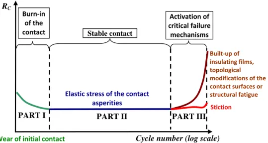
The second important point to be addressed is the reproducibility of the contact resistance over the actuations, and thus along its whole lifetime (cf. Figure 2). The reliability of the switch depends on its ability to withstand some degradations occurring at the contact interface. Three types of phenomena can be studied: the mechanical (cold welding, strain hardening), electrical (arcing, hot welding, annealing) and chemical ones (formation of insulating films at the extreme surface), all inducing modifications of the topological, mechanical and electrical properties of the contact.
Figure 2 :Typical lifetime of micro switches leading to contact failure
As the experimental set-up developed here can be used for studying the fundamental physics of the micro-contact, the understanding of potential failure mechanisms can be made easier if the effort is put upon the identification of the key parameters for each mechanism. In addition, the contact temperature (Tc) of contact a-spots could be linked with the contact force depending on the contact voltage [6]. Indeed the plastic deformation of the asperities during the contact formation proceeds more rapidly when the softening temperature is reached [12]. Thus the effective contact area increases inducing a drop of the contact resistance. However the softening of the metal at the asperities of contact reduces the strain hardening of the a-spots and could accelerate the wear of the contact by the activation of thermal failure mechanisms. Therefore the softening temperature of contact metals is probably one of the most important critical parameter and it has to be studied for reaching a stable and low contact resistance.
3. Experimental techniques
3.1. Description of the experimental set-up
The test described in this paper is based on methods combining a nanoindenter and a high resolution source meter for the determination of the electrical contact resistance versus the contact force and the displacement of the free standing part of the contact. Nanoindentation is firstly designed for material characterization, which is based on the “displacement vs. load” curve obtained by driving a tip into the test material and by monitoring the applied load and the resulting displacement [13]. In our test bench, the nanoindenter’s spherical tip is used as a mechanical actuator. The actuation load is thus reproducible and known with a good accuracy, two points which remain hard to achieve with the actual actuations (for example, electrostatic actuation forces often drift due to dielectric charging [14]).
Built‐up of insulating films, topological modifications of the contact surfaces or structural fatigue
Cycle number (log scale)
Elastic stress of the contact asperities Stiction Stable contact Burn‐in of the contact Activation of critical failure mechanisms
PART I PART II PART III
RC
Figure 3 : Principle of the electrical test performed with a nanoindentation tip
Once the bridge is correctly located under the column of nanoindentation, the tip is brought in contact with the surface of the mobile electrode, and then lowered until mechanical and electrical contact between the bridge and the line. The stiffness of the membrane can be measured in this step [15]. From this moment on, the applied load corresponds to the actuation load of the contact. A schematic view of the set-up can be seen on Figure 3.
The main difficulty for applying a load on test vehicles remains the accurate location of the tip above the contact. This issue has been here overcome by the use of a nanopositionning table achieving a 20nm X-Y resolution in a defined 100μm-side square. Thus, a pseudo-AFM scan is performed by probing the surface with a fixed stiffness of contact between the tip and the surface. The coordinates of the bridge and the line are measured in order to locate the tip just above the contact, that is to say in the middle of the bridge and half-width of the line. An accurate location can then be reached on the scan (cf. Figure 4).
Contact line
Bridge
Location of the tip
Figure 4 : Picture of the scan performed with the nanoindenter on the test structure
The electrical measurements are performed by the use of a four-wires probe: a current flow IC is
applied and the potential drop VC is independently measured. This method for measuring contact
resistance is the same method used in crossed rod contact resistance measurements of Holm [9]: only the contact resistance is measured independently of the voltage drop in the supply wires and access paths. Moreover the environmental chamber allows the control of the temperature of the DUT and of the relative humidity Rh.
3.2. Test vehicle description
Specific test vehicles have been designed for contact analysis, enhancing the extraction of characteristic curves and making possible the comparison between different contact shapes or materials. As illustrated in Figure 5, the tested device is composed of a bridge suspended over a
contact line. A 5µmx5µm square bump is processed underneath. The stiffness of the bridge is about 480 N/m. The contact material is Au-to-Au because gold is the most popular material for electrical contact due to its high conductivity, its high resistance to oxidation and its low propensity to form alien surface films [16].
Figure 5 : Scheme of the test structures
4. FEM modeling of the mechanical actuation 4.1. Point load versus distributed load
Electrostatic actuation is the most widespread actuation modes to deflect a bridge until mechanical and electrical contact with the contact line. This actual actuation principle acts as a distributed pressure on the whole bridge which attracted toward the line by an electrostatic force. During our experiments, this distributed pressure is replaced by a point load applied with the tip of the nanoindenter on the bridge center just above the top of the contact bump.
Bridge (Au)
Bump
Top view
Side view
SiO2
a)
b)
Figure 6 - Vertical stress induced in the bridge and in the bump with a) a local load actuation, b) a distributed pressure actuation. The color bar shows the vertical stress (SY) in MPa.
2D FEM simulations were performed using ANSYS® in order to validate the substitution of the distributed pressure by the point load. This is an important point to be assessed because we tend to mimic the actuation of a real micro switch for easier interpretations of our results. Thus we have to compare the repartition of the vertical stress at contact interface bridge-to-bump. It can be seen on the Figure 6 that the stress repartition is barely similar between the both but the level of stress is higher with the point one. The contact force between the bump and the bridge has been calculated in both cases and is 60 % higher using the point force for a same applied load. It can be assumed that the force dissipated in the anchor is lowered using the point actuation principle. Thanks to these simulations, the point load actuation with the nano indentation tip is validated for this methodology.
4.2. Requirements concerning the tip used
This part will be focused on the comparison between two types of tip: the Berkovitch one (0.320 µm of radius of curvature due to the tip defect) and the spherical one (5.9 µm of radius of curvature).
a)
b)
Figure 7: Vertical stress induced by a) a Berkovitch tip actuation; b) a spherical tip actuation in the bridge and in the bump. The color bar shows the vertical stress (SY) in MPa.
It can be seen on Figure 7.a that the strain of the bridge close to the contact with the Berkovitch tip is higher than the bridge strain at the bump interface.
The stress induced by the Berkovitch tip is 74 % higher and is more localized under the tip than the stress induced by the spherical one. For a same tip displacement, the contact area between the bump and the bridge is 11 % higher using the spherical tip than with the Berkovitch one. The use of a spherical tip allows a better repartition of strain and decreases the stress concentration and plastic deformations under the tip. However the Figure 7.b shows that the deformation of the bridge under the spherical tip cannot be neglected. For that reason, a preliminary test has to be done on the anchors to measure the deformation of the asperities. In that way, the deformation of the bridge can be subtracted to the total deformation.
5. Validation tests
Metal contacting switches have a large and complex set of failure mechanisms driven by the current level. And current is also known to have a primary influence on contact lifetime in macroswitches, with lifetime decreasing at higher current [13][16]. The campaign of tests has been performed on the test vehicles described in the previous part. The obtained results give us the opportunity to regain the behaviour predicted by the previous models. These studies are focused on the self-heating of the
contact with increasing level of current flowing through the contact which is a key issue of contact reliability.
The measurements are performed by sweeping the contact current from 1 mA to 100 mA by measuring the contact voltage in a cold-switching way (actuating the switch while the DC power is off). The impact of current at low- to medium-power levels is investigated to improve understanding of power dissipation at the contact site and more precisely the topological modifications induced. The following results are based on the same 11 successive tests.
5.1. Impact of current at low to medium- levels
Figure 8 shows typical “contact force vs contact resistance” curves for a test structure with a 5 µm² square dimple at 11 different levels of contact current for Au/Au contact. This curves point out the relationship between the contact resistance and the force applied on the contact. These measurements are done with the same bridge-bump pair. The first measurement is performed at 1 mA and then the other ones are done by increasing the current level. When contact is made between the metallic electrodes, the contact force is very low at first and the resistance is high and unstable. At a certain minimum force, depending on the material under investigation, a significant reduction of the resistance occurs. At higher forces the contact is stable and the resistance decreases slightly with further increasing force until reaching saturated regime.
0,5 1,5 2,5 3,5 4,5 5,5 6,5 0 20 40 60 80 100 120 140 160 Contact Force (µN) C o ntac t resistance ( Ω ) I = 1mA I = 10mA I = 20mA I = 30mA I = 40mA I = 50mA I = 60mA I = 70mA I = 90mA I = 80mA I = 100mA
Figure 8 : Contact resistance versus contact force as a function of the contact current
The contact resistances decrease with the increasing contact force as a function of the contact current and can be described by the equation x
C
C AF
R where A and x are constant parameters for each current level. The parameter x decreases from 0.46 to 0.06 when the contact current rises. These values don’t match with equation (1) and (2) because it does not take into account the roughness of the micro-contact surface (cf. Figure 9).
0 0,05 0,1 0,15 0,2 0,25 0,3 0,35 0,4 0,45 0,5 0 10 20 30 40 50 60 70 80 90 100 Current (mA) x
Figure 9 : Evolution of the x parameter versus the contact current for Au/Au contact
The second observation is that the higher the current is, the lower is the dependence of the contact resistance to the load applied. The initial contact resistance remains lower for subsequent cycle at each increasing step of current. The deformations of the contact asperities at the contact closure produce a certain degree of strain hardening of the a-spots. When the softening temperature of the contact material is reached by increasing the level of current, strain hardening disappears in and around the contact interface and the contact area increases. In the same way, the contact area increase can be due to the remove or the breakdown of insulating film on the electrodes because of heating. The presence of alien thin insulating film on the contact surface indeed seems very likely, probably composed of hydrocarbons [17], carbon or sulphur contaminants adsorbed onto the surface [18]. In addition, one cannot exclude the possibility that the contact is not fully metallic and some fraction of the contact is acting as a tunnel conductor. The decrease of the contact resistance with increased current can be also explained if quantum mechanical tunnelling through alien film is the charge transfer mechanism [16]. Indeed the current increase yield to the voltage increase across the contact by Ohms law. Voltage shits the Fermi level up on one side of the film barrier, which allows a net tunnelling current to flow [9]. In the end, assuming the presence of thin insulating layer on the contact surface, more current level increases voltage across the contact, allowing a higher tunnel effect conduction and the breakdown of the insulating film, making easier a higher current flow [19].
To further examine the heating effect on contact resistance, the study is focused on the contact temperature when the maximum contact load is reached. The methodology consists in measuring the contact voltage to deduce the contact temperature using equation 3. The series of tests performed previously will be used to compare the impact of increased contact temperature on the test vehicle. We introduce for this result the power level Pc to make easier the parallel with RF concepts. The power
through the contact is calculated by using the equation Pc RcIc2. Figure 10 shows the contact temperature as a function of the increasing power through the Au/Au contact.
0 20 40 60 80 100 120 0 1 2 3 4 5 6 7 8 9 10 Power level (mW) C o nta c t tem p er atur e (° C )
Figure 10 : Contact temperature versus the power through the contact
The contact resistance continues to decrease keeping the contact temperature roughly constant after reaching the published softening temperature for gold ~100°C [11] (ie. the contact softening) corresponding to a contact voltage of 70-80 mV for contact near room temperature. After reaching the softening temperature from 3 mW, the contact resistance continues to decrease keeping the contact temperature roughly constant. At this point the contact temperature stops to increase and fluctuates between 80°C and 120°C (65 mV to 75 mV). The temperature seems to be stabilized while the power within the contact rises.
5.2. Topological modification of the contact surface
0 1000 2000 3000 4000 5000 6000 7000 8000 -20 -10 0 10 20 30 40 50 60 70 80 90 100 110 120 130 140 Contact force (µN) S ti ff n es s (N/ m ) Figure 11 : Evaluation of the number of asperities
A specific method has been developed to estimate the increase n of the asperities number, based on the mechanical measurements provided by the micro-bending test. When the force is high enough, new asperities come into contact, involving a sudden modification of the loading configuration, that is to say a discontinuity in the stiffness K. The parameter n is then evaluated by counting the number of steps in the “K vs. FC” curve. As shown on the Figure 11, the number of asperities in contact increases
Softening temperature of Au
n=3
I = 70mA I = 80mA I = 90mA I = 100mAn=5
n=7
n=8
with the contact current. Thus the effective contact area increases inducing a drop of the contact resistance. However, we cannot assume that the initial number of asperities is one, that the reason why the real number of asperities in contact cannot be calculated. Nevertheless, any indication of these increases of the contact asperity number is observed in Figure 8, which is the same experiment. The lake of steps in Figure 8 can be explained because mechanical contact does not mean electrical contact. The transition from a mechanical contact to an electrical contact for asperities is a gradual change which is more progressive and thus hard to observe.
Another point is considering a constant contact load, the apparent stiffness decreases when the electrical current increases. (cf. Figure 11). Such a behaviour indicates insofar as K = FC/d, that the
displacement of the tip is greater at higher current. Softening temperature is indeed reached and the rise of the electrical current implies then a softening of the contact material. When considering a constant contact force, the resulting deformation of the asperities is higher, and the number of "a-spots" grows up. Finally, this decrease in the contact stiffness indicates that structural fatigues of the contact asperities has occurred with repeated actuations.
6. Conclusions
The presented tests and models bring to light the relevance and the validity of this methodology to investigate the micro-contact physics. The origin of this contact resistance reduction is thermally induced with the increase of the contact temperature with the current until reaching the softening temperature. Thus the annealing of the contact leads to a reduction of the contact hardness and the roughness of the contact is lowered after softening of the surfaces. Thereby, the deformation of the contact asperities is higher with increased current making easier the breakdown of residual insulating films, and enlarging the total contact area. At the same time, increased tunneling through an alien film may be in part responsible for these trends. However, the variation of the contact resistance is determined by a competition between asperities flattening, which lowers the contact resistance and heating, which can affect the topography of the contact surface by the activation of thermal failure mechanisms.
The presented test vehicles could be manufactured for future work with several contact materials, which mainly govern the robustness of the contact. The knowledge gained will be the identification of the specific failure mechanisms for each contact design in order to bring recommendations for further improvements of the contact reliability.
7. References
[1] Rebeiz, GM and Muldavin, JB , “RF MEMS switches and switch circuits”, IEEE Microwave magazine, vol. 2, no. 4, pp. 59--71, 2001
[2] Kataoka, K. and Itoh, T. and Suga, T. and Inoue, K., “Contact properties of Ni micro-springs for MEMS probe card”, Proceedings of the 50th IEEE Holm Conference on Electrical Contacts, pp. 231-235, 2004
[3] Pruitt, BL and Park, W.T. and Kenny, TW, “Measurement system for low force and small displacement contacts”, Journal of Microelectromechanical Systems, vol. 13, no. 2, pp. 220-229, 2004
[4] Wang, F., Li, X. and Feng, S., “Micro-cantilever probe cards with silicon and nickel composite micromachining technique for wafer-level burn-in testing”, IEEE Transactions on Advanced Packaging, vol. 32, no. 2, pp. 468-477, 2009.
[5] Gilbert, K.W., Mall, S., Leedy, K.D. and Crawford, B., ”A Nanoindenter Based Method for Studying MEMS Contact Switch Microcontacts”, Proceedings of the 54th IEEE Holm Conference on Electrical Contacts, pp 137-144, 2008
[6] Kwon, H., Jang, S.S., Park, Y.H., Kim, T.S., Kim, Y.D., Nam, H.J. and Joo, Y.C., “Investigation of the electrical contact behaviours in Au-to-Au thin-film contacts for RF MEMS switches”, Journal of Micromechanics and Microengineering, no. 18, pp 1-9, 2008
[7] Yang, Z. and Lichtenwalner, D. and Morris, A. and Menzel, S. and Nauenheim, C. and Gruverman, A. and Krim, J. and Kingon, AI, “A new test facility for efficient evaluation of
MEMS contact materials”, Journal of Micromechanics and Microengineering, no. 17, pp 1788-1795, 2007
[8] F. Solazzi, et al., “Contact Modelling of RF MEMS Switches Based On FEM Simulations”, Proceedings of the 10th International Symposium on RF MEMS and RF Microsystems, pp 173-176, 2009
[9] R. Holm, “Electrical Contacts-Theory and Applications,” 4th ed. Berlin Germany: Springer-Verlag, 1967.
[10] Cédric Seguineau, Adrien Broue, Jérémie Dhennin, Jean-Michel Desmarres, Arnaud Pothier, Xavier Lafontan, Michel Ignat. “Mechanical Cycling for electrical performances of materials
used in MEMS: Application to gold micro-switches”, Metals Materials And Processes, no.1, pp. 1-24, 2008
[11] Jensen, B.D., Chow, LL, Huang, K., Saitou, K., Volakis, J.L. and Kurabayashi, K., “Effect of nanoscale heating on electrical transport in RF MEMS switch contacts” in Journal of microelectromechanical systems, vol. 14, no. 5, pp. 935-946, 2005.
[12] Fortini, A., Mendelev, M.I., Buldyrev, S. and Srolovitz, D., “Asperity contacts at the nanoscale: comparaison of Ru and Au,” in Journal of Applied Physics, vol. 104, no. 7, pp. 4320, 2008
[13] Oliver, W.C., Pharr, G.M., “An Improved technique for determining hardness and elastic modulus using load and displacement sensing indentation experiments”, J. Mater. Res., vol. 7, no. 6, 1992.
[14] Melle, S., Dubuc, D.M.L., Grenier, D., Bary, K., Plana, L., Vendier, R., Muraro, O. and Cazaux, JL, “Modeling of the dielectric charging kinetic for capacitive RF-MEMS”, IEEE MTT-S International Microwave MTT-Symposium digest, pp. 4, 2005
[15] Seguineau, C., Desmarres, J-M., Dhennin, J., Lafontan, X. and Ignat, M., “MEMS Reliability : Accurate Measurements of beam stiffness using nanoindentation techniques”, Proceeding of CANEUS 2006, pp. 11057, 2006
[16] Patton, ST and Zabinski, JS., “Fundamental studies of Au contacts in MEMS RF switches,” in Tribology Letters, vol. 18, pp 215-230, 2005.
[17] Tringe, JW and Uhlman, TA and Oliver, AC and Houston, JE, “A single asperity study of Au/Au electrical contacts”, Journal of Applied Physics, vol. 93, pp. 4661, 2003
[18] Ma, Q. and Tran, Q. and Chou, T.K.A. and Heck, J. and Bar, H. and Kant, R. and Rao, V., “Metal contact reliability of RF MEMS switches”, Reliability, Packaging, Testing, and Characterization of MEMS/MOEMS VI, Proceedings of the SPIE, vol.6463, pp. 646305-646305, 2007
[19] Jackson, RL and Kogut, L., “Electrical contact resistance theory for anisotropic conductive films considering electron tunnelling and particle flattening”, IEEE Transactions on Components and Packaging Technologies, vol. 30, no. 1, pp 59-66, 2007