Creating Sub-50 Nm Nanofluidic Junctions in PDMS Microfluidic
Chip via Self-Assembly Process of Colloidal Particles
The MIT Faculty has made this article openly available.
Please share
how this access benefits you. Your story matters.
Citation
Xi, Wei, Abeer Syed, Pan Mao, Jongyoon Han, and Yong-Ak Song.
"Creating Sub-50 Nm Nanofluidic Junctions in PDMS Microfluidic
Chip via Self-Assembly Process of Colloidal Particles." JOVE:
Engineering 109: e54145 (2016).
As Published
http://dx.doi.org/10.3791/54145
Publisher
MyJoVE Corporation
Version
Final published version
Citable link
http://hdl.handle.net/1721.1/102694
Terms of Use
Article is made available in accordance with the publisher's
policy and may be subject to US copyright law. Please refer to the
publisher's site for terms of use.
Video Article
Creating Sub-50 Nm Nanofluidic Junctions in PDMS Microfluidic Chip via
Self-Assembly Process of Colloidal Particles
Xi Wei1,2, Abeer Syed1, Pan Mao3, Jongyoon Han4, Yong-Ak Song1,2
1Division of Engineering, New York University Abu Dhabi (NYUAD)
2Department of Chemical and Biomolecular Engineering, New York University Tandon School of Engineering 3Newomics, Inc.
4Department of Electrical Engineering and Computer Science, Department of Biological Engineering, MIT
Correspondence to: Yong-Ak Song at rafael.song@nyu.edu URL: http://www.jove.com/video/54145
DOI: doi:10.3791/54145
Keywords: Engineering, Issue 109, Ion concentration polarization (ICP), self-assembly process, silica colloids, nanofluidics, microfluidics, electrokinetic concentration
Date Published: 3/13/2016
Citation: Wei, X., Syed, A., Mao, P., Han, J., Song, Y.A. Creating Sub-50 Nm Nanofluidic Junctions in PDMS Microfluidic Chip via Self-Assembly Process of Colloidal Particles. J. Vis. Exp. (109), e54145, doi:10.3791/54145 (2016).
Abstract
Polydimethylsiloxane (PDMS) is the prevailing building material to make microfluidic devices due to its ease of molding and bonding as well as its transparency. Due to the softness of the PDMS material, however, it is challenging to use PDMS for building nanochannels. The channels tend to collapse easily during plasma bonding. In this paper, we present an evaporation-driven self-assembly method of silica colloidal nanoparticles to create nanofluidic junctions with sub-50 nm pores between two microchannels. The pore size as well as the surface charge of the nanofluidic junction is tunable simply by changing the colloidal silica bead size and surface functionalization outside of the assembled microfluidic device in a vial before the self-assembly process. Using the self-assembly of nanoparticles with a bead size of 300 nm, 500 nm, and 900 nm, it was possible to fabricate a porous membrane with a pore size of ~45 nm, ~75 nm and ~135 nm, respectively. Under electrical potential, this nanoporous membrane initiated ion concentration polarization (ICP) acting as a cation-selective membrane to concentrate DNA by ~1,700 times within 15 min. This non-lithographic nanofabrication process opens up a new opportunity to build a tunable nanofluidic junction for the study of nanoscale transport processes of ions and molecules inside a PDMS microfluidic chip.
Video Link
The video component of this article can be found at http://www.jove.com/video/54145/
Introduction
Nanofluidics is an emerging research area of µTAS (Micro Total Analysis Systems) to study biological processes or transport phenomena of ions and molecules at the length scale of 101- 102 nm. With the advent of the nanofluidic tools such as nanochannels, transport processes of molecules and ions can be monitored with unprecedented precision and manipulated, if needed, by exploiting features that are available only at this length scale for separation and detection.1,2 One of these characteristic nanoscale features is a high ratio of surface to bulk charge (or Dukhin number) in nanochannels that can cause a charge imbalance and initiate ion concentration polarization (ICP) between the nanochannel and microchannel.3
A common device platform for the study of nanofluidic phenomena consists of a two-microchannel system connected by an array of nanochannels as a junction.4-6 The material of choice for building such a nanofluidic device is the silicon because of its high stiffness that
prevents the channel from collapsing during bonding processes.7 However, silicon device fabrication requires expensive masks and substantial amount of processing in the cleanroom facility.8-10 Due to the convenience of device fabrication through molding and plasma bonding,
polydimethylsiloxane (PDMS) has widely been accepted as a building material for microfluidics and it would be an ideal material for nanofluidics as well. However, its low Young's modulus around 360-870 KPa, makes the PDMS channel easily collapsible during plasma bonding. The minimum aspect ratio of the nanochannel (width to depth) has to be less than 10:1 which means that the fabrication of PDMS devices via standard photolithography will become extremely challenging if the nanochannel depth has to be below 100 nm, requiring a channel width less than the current limit of photolithography at around 1 µm. To overcome this limitation, there have been attempts to create nanochannels in PDMS using non-lithographical methods such as stretching to initiate cracks with mean depth of 78 nm11 or to form wrinkles after plasma treatment.12 Collapsing a PDMS channel with mechanical pressure allowed a nanochannel height as low as 60 nm.13
Even though these highly inventive non-lithographic methods allowed building nanochannels below 100 nm in depth, the dimensional
controllability of the nanochannel fabrication still poses an obstacle to a wide acceptance of PDMS as a building material for nanofluidic devices. Another critical problem of the nanochannels, whether in silicon or PDMS, is the surface functionalization in case there is a need to alter the surface charge on the channel wall for the manipulation of ions or molecules. After device assembly through bonding, the nanochannels are extremely difficult to reach for surface functionalization due to the diffusion-limited transport. To create a nanoscale channel with high
dimensional fidelity and facile surface functionalization, the self-assembly method of colloidal particles induced by evaporation14-16 in microfluidic
devices can be one of the promising approaches. Besides the controllability of pore size and surface property, there is even a possibility to tune the size of the pore in-situ when using colloidal particles coated with polyelectrolytes by controlling temperature,17 pH,18,19 and ionic strength.18 Because of these advantages, the self-assembly method of colloidal particles has already found applications for electrochromatography,20
biosensors,21 protein concentration22 and separation of proteins and DNA in microfluidics.14,23 In this study, we deployed this self-assembly method to build an electrokinetic preconcentration device in PDMS that requires a nanofluidic junction between two microchannels.24 The
fundamental mechanism behind the electrokinetic concentration is based on ion concentration polarization (ICP).25 A detailed description of fabrication and assembly steps is included in the following protocol.
Protocol
1. Preparation of the Silica Colloidal Bead Suspensions
1. Preparation of 300 nm and 500 nm silica bead suspensions
1. Vortex the silica bead stock suspension (10% w/v in water) for 30 sec. to obtain a homogeneous suspension. Pipette a total of 600 µl stock suspension into a 1.5 ml tube and centrifuge it at 2,600 x g for 1 min.
2. Substitute the supernatant with 400 µl of 1 mM sodium phosphate buffer (PB, pH 7.0).
3. Suspend the silica beads into a final concentration of 15% in 1 mM sodium phosphate solution at pH 7.0 through vortexing. 2. Surface functionalize 500 nm silica carboxyl beads with poly(allylamine hydrochloride, PAH), and with poly(sodium styrene
sulfonate, PSS) polyelectrolytes
1. Suspend 0.1 g of 500 nm silica beads with carboxyl group with 10 ml 1 M NaCl (pH 7.0) for 1 % (w/v) bead suspension.
2. Prepare 0.4% PAH (MW 65K) in 1 M NaCl by dissolving 300 µl of the stock solution (20% w/v in water) in 15 ml of 1 M NaCl. Prepare 0.9% PSS (MW 70K) in 1 M NaCl solution by dissolving 0.18 g PSS in 20 ml 1 M NaCl solution. Vortex both solutions for 1 min. to dissolve the polyelectrolytes completely.
3. Add 200 µl of PAH solution to 9.8 ml of 1% silica carboxyl beads in a 15 ml tube to deposit a positively charged polyelectrolyte layer on silica beads with carboxyl functional group. Vortex the bead suspension for 1 min. and incubate it on a tube rotator for 60 min. at RT. 4. Centrifuge the bead suspension at 1801 x g for 1 min. and wash off the unbound PAH five times with 10 ml DI water. After each
centrifuge and removal of the supernatant, the beads were densely packed at the bottom of the tube. Disrupt the bead clump by vigorous pipetting with 2 ml of DI water before adding 8 ml of DI water so that the beads can be re-suspended and washed off prior to the next centrifuge step.
5. Follow the steps in 1.2.3 and 1.2.4 for PSS coating to deposit a negatively charged layer on the beads. Re-suspend the beads in 9.8 ml of 1 M NaCl prior to the PSS deposition after removing the DI water supernatant from the 5th washing step of 1.2.4.
1. Use the same vigorous pipetting step using 2 ml of 1 M NaCl to break up the bead clump at the bottom of the 15 ml tube and then add 8 ml of 1 M NaCl. Add 200 μl of PSS solution to 9.8 ml of the silica beads deposited with a single PAH layer. After vortexing for 1 min. and incubation for 60 min. on the tube rotator, repeat 5 washing steps with DI water.
2. Measure the zeta potential of the beads before and after each polyelectrolyte coating using a dynamic light scattering system according to manufacturer's protocol to verify the polyelectrolyte deposition procedure has been performed correctly (see Table 1).
6. Repeat five washing steps with DI water following the single PSS layer deposition and re-suspend the beads in 650 µl of 1 mM sodium phosphate buffer with 0.05% Tween 20 (15% w/v) prior to use in the microfluidic device to enhance its flowability.
3. Follow the procedure described above from 1.2.5 to 1.2.6 for 500 nm silica beads with amine functional group to deposit a single layer of PSS.
2. Fabrication of the PDMS Microfluidic Chip
1. Microfabrication of the silicon master
1. Fabricate the silicon master for PDMS molding using microfabrication techniques as follows.
1. Spin coat a 1 µm thin photoresist at 4,000 rpm on a silicon wafer. Pattern the layer using projection lithography (exposure time 170 msec.) and etch 700 nm deep and 2 µm wide planar nanochannels (acting as nanotraps for the silica beads) with reactive ion etching.
2. Use the following etching parameters to achieve an etch rate of 3.5 nm/s: CHF3 (45 sccm), CF4 (15 sccm), Ar (100 sccm),
pressure 100 mTorr, RF power 200 W.
2. Spin coat the second 1 μm thick photoresist layer at 2,000 rpm and perform an alignment to the previously patterned nanotraps. Pattern the microchannels via contact lithography and by deep reactive ion etching (DRIE) of silicon. Use the DRIE parameters26 in
Table 2.
2. Fabrication of PDMS mold
1. Silanize the silicon master with trichlorosilane (50 μl) in a vacuum jar O/N.
CAUTION: Tricholorosilane is a toxic and corrosive material. Always use it in a chemical hood with proper personal protection equipment.
2. Mix the base to the curing agent at 10:1 ratio and cast PDMS on the silanized silicon master and cure it at 70 °C for 2 hr in a convection oven.
3. Remove the PDMS slab from the silicon master with a knife and plasma bond it on a blank wafer using a plasma cleaner after a plasma treatment in a plasma cleaner for 1 min. Attach tapes along the edge to mark a partition line for the following PDMS casting step.
4. Silanize the PDMS mold in a vacuum jar with trichlorosilane (50 μl) O/N.
5. Cast PDMS (base: curing agent at 10:1 ratio) on the silanized PDMS mold and cure it at 70 °C for 2 hr in a convection oven. 3. Fabrication of the PDMS device
1. Peel off the cured PDMS slab from the PDMS mold along the partition line marked with the tape.
2. Punch reservoir holes with 1.5 mm biopsy punch, clean with a tape, rinse with isopropyl alcohol (IPA) and dry with nitrogen. 3. Plasma bond the PDMS device on a 25 mm x 75 mm microscope glass slide after a plasma treatment in a plasma cleaner for 1 min. 4. Ultrasonicate the bead suspension for 60 min. in an ultrasonic bath prior to filling. Pipette a 10 µl bead suspension (300 nm
non-functionalized silica beads, or 500 nm silica carboxyl beads with PAH-PSS layers, or 500 nm silica amine beads with a PSS layer) into the inlets 4 and 6 each (see Figure 1 A, B) immediately after plasma bonding of the PDMS chip to a glass substrate. Tap gently on the PDMS
chip with a pipette tip to enhance the bead packing.
1. After filling the bead delivery channels, cover all the inlets except for 1 and 9 with tape. Air-dry the device for 3 hr and store at +4 °C prior to use. Figure 2 gives a step-by-step schematic of the colloidal self-assembly process.
3. Experiment for Electrokinetic Concentration of DNA
1. Fill the reservoirs 3, 7 with a buffer solution (10 μl of 1 mM PB) and reservoir 5 with a DNA sample (10 μl of 10 nM in 1 mM PB) and apply a gentle negative pressure with an inverted pipette tip on reservoirs 2, 8 and 10 to fill the channels with the solutions without bubbles (see
Figure 1B).
2. Add 10 μl of 1 mM PB to reservoirs 2 and 8 and 10 μl of 10 nM DNA to reservoir 10 to balance the pressure and wait for 5 min. to reach equilibrium.
3. Insert the Pt wires into reservoirs 3, 5, 7, 10.
4. Apply voltage across the nanofluidic junction using a voltage divider connected to a source meter and Pt wires. First apply 30 V on reservoirs 5, 10 and GND on reservoirs 3, 7.
5. Decrease the voltage to 25 V on reservoir 10 after ~30 sec.
6. Use a mechanical shutter with a periodic opening in every 5 s to minimize photobleaching of the sample when recording the fluorescence signals from the DNA.
Representative Results
An electrokinetic concentrator chip in PDMS that contains a self-assembled nanofluidic junction between two microchannels is shown in Figure 1A). The channel in the middle of the device is filled with a DNA sample solution and flanked by two buffer solution channels on each side via a
50 µm wide bead delivery channel (Figure 1B). The silica colloidal suspension is flown into the bead delivery channel immediately after plasma
bonding to create a nanofluidic junction between the sample and the buffer solution channel. The nanotrap array consisting of 700 nm deep and 2 μm wide nanochannels is used to trap the colloidal particles. Its scanned image obtained with a non-contact surface profiler is shown in Figure 1C). The colloidal bead membranes after evaporation are shown in Figure 1D). The SEM in Figure 1E) shows the silica beads trapped at the
planar nanotrap array separating the sample channel from the bead delivery channel. The 300 nm silica bead packing shows highly ordered hexagonal packing with some minor defects that could cause a variation in the concentration behavior (Figure 1F). The design of the PDMS
Figure 1. Microfluidic concentrator in PDMS with an integrated sub-50 nm nanoporous junction. (A) Photo of the PDMS concentrator
device. (B) Schematic of the micro-nanofluidic device with a bead delivery channel between the sample and buffer solution channel. The voltage
is applied across the bead membranes between the sample channel and the buffer solution channels. (C) Surface profile of the nanotrap array
in PDMS with a width of 2 μm and a depth of 700 nm. (D) Micrograph of the device with a colloidal particle assembly inside the bead delivery
channel after evaporation. (E) Scanning electron micrograph of the self-assembled 300 nm silica colloidal particles with the nanotrap arrays
between the sample and buffer channel. The 300 nm beads are trapped at the entrance of the nanotraps due to surface tension. (F) Hexagonally
packed 300 nm silica beads inside the bead delivery microchannel after evaporation. (Adapted from Ref. 25 with permission from The Royal
Society of Chemistry) Please click here to view a larger version of this figure.
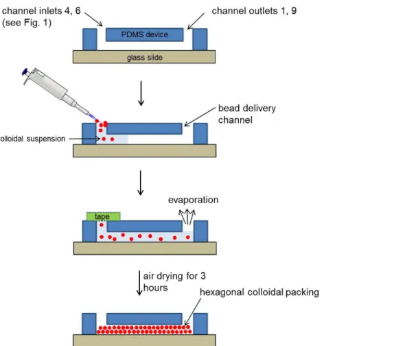
A schematic of the microfabrication steps for the PDMS concentrator device is shown in Figure 2. To make a PDMS device, a double PDMS
casting is required. The bead filling process in the PDMS concentrator is shown in Figure 3. The details for the microfabrication and the filling
Figure 2. Schematic of the fabrication process for the silicon master, the PDMS master and the PDMS concentrator device. After two
photolithographic and etching steps, the silicon master is cast with PDMS. After a double-molding, the PDMS device is assembled via plasma bonding and filled with a bead suspension. Please click here to view a larger version of this figure.
Figure 3. Step-by-step schematic for self-assembly of colloidal silica beads. 10 µl of the bead suspension was pipetted in to the bead
delivery channels immediately after plasma treatment. Once the bead delivery channel was filled, all but two inlets 1 and 9 were covered with tape and the devices air dried for 3 hr prior to use. (Reproduced from Ref. 25 with permission from The Royal Society of Chemistry) Please click
Colloidal particles (500 nm) Zeta potential (mV)
Silica -2.04
Silica amine 19.6
Silica carboxyl -19.73
Silica carboxyl, PAH coated 31.8
Silica carboxyl, PAH, PSS coated -28.5
Silica amine, PSS coated -31.2
Table 1. Zeta potential of silica beads at 25 °C. 0.1% (w/v) colloidal solutions were used for the measurements (n=3).
The SEM images taken from the bead packing channel after drying out show a pore size ranging between 60 nm, 91 nm and 170 nm, as shown in Figure 4. The pore size corresponds to approximately 20% of the bead size, 300 nm, 500 nm and 900 nm, respectively (15% of the bead
diameter is the theoretical pore size).
Figure 4. SEM images of self-assembled 300 nm (A), 500 nm (B) and 900 nm (C) silica colloidal bead packing. PDMS devices were
reversibly bonded to glass slides and beads flown into the channel using negative pressure. After air-drying the devices O/N, the PDMS devices were peeled of the glass carefully and imaged. This pore sizes were estimated to be 60±2, 91±5 and 170±7 nm for 300 nm, 500 nm and 900 nm beads respectively (n=9). These pore sizes were close to the theoretical size, ~15% of the bead diameter. (Adapted from Ref. 25 with permission from The Royal Society of Chemistry) Please click here to view a larger version of this figure.
When applying voltage of 30 V across the 300 nm bead membrane, an ion depletion zone was observed near the colloidal membrane inside a microchannel filled with a fluorescent labeled DNA (Figure 5 A, B). When lowering the voltage to 25 V on the left side, the DNA molecules got
accumulated in the form of a plug and its concentration increased due to electroosmotic flow driven by a voltage difference of 30 V- 25 V across the sample channel (Figure 5 C, D).
Figure 5. Time-lapse micrographs show the formation of an ion depletion region near the nanofluidic colloidal junctions in the channel filled with DNA (initial concentration of 10 nM). The ion depletion region was initiated at t=10 s and a concentrated DNA plug was generated
at V2 = 30 V and V1 = 25 V across the sample channel while the buffer channels were grounded. The dotted lines have been used to highlight the channels walls. A concentration factor of ~1,700 folds was achieved within 15 min. using a 300 nm colloidal membrane. (Reproduced from Ref. 25 with permission from The Royal Society of Chemistry) Please click here to view a larger version of this figure.
The silica membranes with a bead size of 300 nm and 500 nm showed the highest concentration factor at ~1,700 times for the Cy 5 tagged DNA (CAA CCG ATG CCA CAT CAT TAG CTA C) within 15 min. (Figure 6 A, B). The polyelectrolyte-coated silica bead membranes led to a 200- to
1,000-fold increase in the DNA concentration after 15 min. (Figure 6 C, D).
Figure 6. Fluorescence intensity of DNA as a function of time for (A) 300 nm silica beads (B) 500 nm silica beads and (C) 500 nm PSS-coated silica amine beads and (D) 500 nm PAH/PSS PSS-coated silica carboxyl beads. The dotted lines represent the fluorescence signal
intensity level for 10 nM (A, B , C, D), 17 µM (A, B), 2 µM (C) and 10 µM (D) DNA. The results have been normalized against background
fluorescence. (Reproduced from Ref. 25 with permission from The Royal Society of Chemistry) Please click here to view a larger version of this
figure.
Process time Etch mode Passivation mode
Process time 6 s 4.5 s
Overrun 0.5 s 0 s
Platen generator Power 80 W 60 W
Coil generator Power 600 W 600 W
Gas SF6 70 sccm C4F8 35 sccm
Etch rate 1.47 µm/min
Table 2. DRIE parameters.
Discussion
Following the common device design scheme to study nanofluidics, we fabricated a nanofluidic junction between two microfluidic channels by using the evaporation-driven self-assembly of colloidal nanoparticles instead of lithographically patterning an array of nanochannels. When flowing the colloidal particles into the bead delivery channel, an array of nanotraps with a depth of 700 nm and a width of 2 µm on both sides of the bead delivery channel at a total width of 100 μm prevented the bead suspension from flowing into the buffer and sample channel due to the surface tension at the nanotraps. Once trapped, the colloidal particles packed in the bead delivery channel rapidly and formed a nanoporous junction between the sample and buffer channel.
It is important to load the bead suspension immediately after plasma bonding so that the capillary force drives the silica bead suspension up to the entrance of the outlet reservoirs in the temporarily hydrophilic bead delivery channel. In order to prevent an air bubble blocking the flow in the inlet reservoir, it is highly recommended to reach the bottom of the reservoir with a pipette tip and then release the bead suspension into the reservoir. In the case of the surface-functionalized beads with polyelectrolytes, their flowability was drastically reduced compared to the silica beads without surface functionalization and tended to aggregate more easily and adhere to the channel surface during the filling process. In order to prevent a clogging of the channel with the polyelectrolyte-coated beads, we added a surfactant, 0.05% Tween 20, to the bead suspension. In case there was still a clogging problem during filling, a gentle tapping on the PDMS chip with a pipette tip generally helped to resolve it.
Also, it is important that the bead suspension was not completely dried out after evaporation since it would be difficult to infiltrate the bead membrane with the sodium phosphate buffer solution again. Therefore, after 3 hr of partial evaporation, all in- and outlets of the PDMS device
were taped and kept at 4 °C for storage prior to use so the bead packing stays moist. During the preconcentration experiments, the self-assembled bead maintained its structural stability for the most part. However, in few instances, we observed a dislocation of the beads which indicated a defective packing of the beads in microchannels. The self-assembled silica beads ranging from a diameter of 900 nm down to 300 nm after the self-assembly can be seen in Figure 4. The theoretical pore size of the bead packing was ~45 nm, approximately ~15% of the colloidal particle diameter. We could confirm the pore size using a SEM analysis and measured a pore size approximately 20% of the bead diameter after packing.
Using the self-assembled 300 nm and 500 nm colloidal particle membranes as an ion-selective nanoporous junction, we could initiate ion depletion region at 30 V and concentrate 10 nM Cy5 tagged DNA (CAA CCG ATG CCA CAT CAT TAG CTA C) in 1 mM sodium phosphate buffer (Figure 5). By continuously flowing the DNA sample towards the ion depletion zone with an electroosmotic flow at a voltage difference V2-V1 =5 V, we could increase the initial DNA concentration by ~1,700 folds within 15 min. (Figure 6a, b). 500 nm beads allowed more robust
DNA concentration than 300 nm beads, as shown in Figure 6b). Since the electrokinetic concentration is based on a force balance between the electroosmotic force and the highly nonlinear electrophoretic forces, the resulting concentration factor is determined by the degree to which this force balance can be maintained during electrokinetic concentration.27
Another significant advantage of deploying the colloidal particles for building a nanofluidic junction is the ease with which its surface functionalization can be performed. Instead of creating a nanochannel through bonding first and then performing a surface functionalization on it, we can simply surface functionalize the colloidal particles in a vial outside of the device first and then flow them into the channel for self-assembly. Based on this approach, we could initiate ICP using the 500 nm silica amine particles coated with a single layer of PSS and 500 nm silica carboxyl particles coated with a layer of PAH and PSS (Figure 6 c and d), at lower voltages (8 V and 10 V, respectively) than the colloidal particles without surface functionalization (30 V). This result shows that the surface functionalization of the colloidal particles prior to the self-assembly was effective to increase the surface charge of colloidal particles and resulted in higher ICP. However, in terms of the concentrator factor obtained, the nanofluidic junction of the surface functionalized beads was less effective than the non-functionalized silica beads. The amine/PSS-coated beads enabled a factor of ~200, while the carboxyl/PAH/PSS bead membrane showed a 1,000-fold increase after 15 min. (Figure 6d). This result can be explained by a higher surface charge of the surface functionalized nanopores that led to an increased length of the ion depletion region pushing the sample concentration plug farther away from the bead membrane and therefore, to less stable concentration. We believe that shortening the total width of the nanoporous bead membrane from currently 1 mm (the section of the bead membrane parallel to the sample channel) could mitigate this instability issue. According to our previous study, the width of the nanoporous junction determines the amount of ionic current passing through it.28 As the width increases, the ionic current increases and since more cations can migrate through the membrane, the depletion length increases and the concentration plug is further pushed away from the nanoporous junction. Therefore, the accumulation occurs in a less confined manner and the sample plug becomes less stable. Empirically, the nanoporous junction should be ~100-400 µm in width. Another feature to improve was an insufficient thickness of the PDMS wall of 15 µm between the sample channel and the bead delivery. This thin PDMS section led to an insufficient bonding that enabled an ionic current between the buffer and sample channel. Therefore, the entire bead membrane section parallel to the sample channel (1 mm in width) was acting as a nanoporous junction, even though only 100 μm of the bead was intended as a nanoporous junction membrane according to the total width of the nanotrap array. The PDMS wall thickness should be at least 25 µm or higher.
Disclosures
The authors have nothing to disclose.
Acknowledgements
This work was supported by NIH R21 EB008177-01A2 and New York University Abu Dhabi (NYUAD) Research Enhancement Fund 2013. We express our thanks to the technical staff of MIT MTL for their support during microfabrication and James Weston and Nikolas Giakoumidis of NYUAD for their support in taking SEM pictures and building a voltage divider, respectively. The device fabrication in PDMS was conducted in the microfabrication core facility of NYUAD. Lastly, we would like to thank Rebecca Pittam from the NYUAD Center for Digital Scholarship for video shooting and editing.
References
1. Mawatari, K., Kazoe, Y., Shimizu, H., Pihosh, Y., & Kitamori, T. Extended-Nanofluidics: Fundamental Technologies, Unique Liquid Properties, and Application in Chemical and Bio Analysis Methods and Devices. Anal Chem. 86, 4068-4077, (2014).
2. Tsukahara, T., Mawatari, K., & Kitamori, T. Integrated extended-nano chemical systems on a chip. Chem Soc Rev. 39, 1000-1013, (2010).
3. Mani, A., Zangle, T. A., & Santiago, J. G. On the Propagation of Concentration Polarization from Microchannel-Nanochannel Interfaces Part I: Analytical Model and Characteristic Analysis. Langmuir. 25, 3898-3908, (2009).
4. Aizel, K. et al. Enrichment of nanoparticles and bacteria using electroless and manual actuation modes of a bypass nanofluidic device. Lab
Chip. 13, 4476-4485, (2013).
5. Wang, Y. C., Stevens, A. L., & Han, J. Million-fold preconcentration of proteins and peptides by nanofluidic filter. Anal Chem. 77, 4293-4299,
(2005).
6. Karnik, R. et al. Electrostatic control of ions and molecules in nanofluidic transistors. Nano letters. 5, 943-948, (2005).
7. Mao, P., & Han, J. Y. Fabrication and characterization of 20 nm planar nanofluidic channels by glass-glass and glass-silicon bonding. Lab
Chip. 5, 837-844, (2005).
8. Mao, P., & Han, J. Massively-parallel ultra-high-aspect-ratio nanochannels as mesoporous membranes. Lab Chip. 9, 586-591, (2009).
9. Balducci, A., Mao, P., Han, J. Y., & Doyle, P. S. Double-stranded DNA diffusion in slitlike nanochannels. Macromolecules. 39, 6273-6281,
10. Yamada, M., Mao, P., Fu, J. P., & Han, J. Y. Rapid Quantification of Disease-Marker Proteins Using Continuous-Flow Immunoseparation in a Nanosieve Fluidic Device. Anal Chem. 81, 7067-7074, (2009).
11. Huh, D. et al. Tuneable elastomeric nanochannels for nanofluidic manipulation. Nat Mater. 6, 424-428, (2007).
12. Chung, S., Lee, J. H., Moon, M. W., Han, J., & Kamm, R. D. Non-lithographic wrinkle nanochannels for protein preconcentration. Adv Mater.
20, 3011-3016, (2008).
13. Park, S. M., Huh, Y. S., Craighead, H. G., & Erickson, D. A method for nanofluidic device prototyping using elastomeric collapse. Proc Natl
Acad Sci. 106, 15549-15554, (2009).
14. Zeng, Y., & Harrison, D. J. Self-assembled colloidal arrays as three-dimensional nanofluidic sieves for separation of biomolecules on microchips. Anal Chem. 79, 2289-2295, (2007).
15. Malekpourkoupaei, A., Kostiuk, L. W., & Harrison, D. J. Fabrication of Binary Opal Lattices in Microfluidic Devices. Chem Mat. 25, 3808-3815,
(2013).
16. Merlin, A., Salmon, J.-B., & Leng, J. Microfluidic-assisted growth of colloidal crystals. Soft Matter. 8, 3526-3537, (2012).
17. Schepelina, O., & Zharov, I. PNIPAAM-modified nanoporous colloidal films with positive and negative temperature gating. Langmuir. 23,
12704-12709, (2007).
18. Schepelina, O., & Zharov, I. Poly(2-(dimethylamino)ethyl methacrylate)-Modified Nanoporous Colloidal Films with pH and Ion Response.
Langmuir. 24, 14188-14194, (2008).
19. Smith, J. J., & Zharov, I. Ion transport in sulfonated nanoporous colloidal films. Langmuir. 24, 2650-2654, (2008).
20. Gaspar, A., Hernandez, L., Stevens, S., & Gomez, F. A. Electrochromatography in microchips packed with conventional reversed-phase silica particles. Electrophoresis. 29, 1638-1642, (2008).
21. Lee, S. Y. et al. High-Fidelity Optofluidic On-Chip Sensors Using Well-Defined Gold Nanowell Crystals. Anal Chem. 83, 9174-9180, (2011).
22. Hu, Y. L. et al. Interconnected ordered nanoporous networks of colloidal crystals integrated on a microfluidic chip for highly efficient protein concentration. Electrophoresis. 32, 3424-3430, (2011).
23. Zhang, D.-W. et al. Microfabrication-free fused silica nanofluidic interface for on chip electrokinetic stacking of DNA. Microfluid Nanofluid. 14,
69-76, (2013).
24. Syed, A., Mangano, L., Mao, P., Han, J., & Song, Y. A. Creating sub-50 nm nanofluidic junctions in a PDMS microchip via self-assembly process of colloidal silica beads for electrokinetic concentration of biomolecules. Lab Chip. 14, 4455-4460, (2014).
25. Kim, S. J., Song, Y. A., & Han, J. Nanofluidic concentration devices for biomolecules utilizing ion concentration polarization: theory, fabrication, and applications. Chem Soc Rev. 39, 912-922, (2010).
26. Fu, J. P., Mao, P., & Han, J. Y. Continuous-flow bioseparation using microfabricated anisotropic nanofluidic sieving structures. Nat Protoc. 4,
1681-1698, (2009).
27. Plecis, A., Nanteuil, C., Haghiri-Gosnet, A. M., & Chen, Y. Electropreconcentration with Charge-Selective Nanochannels. Anal Chem. 80,
9542-9550, (2008).
28. Ko, S. H. et al. Nanofluidic preconcentration device in a straight microchannel using ion concentration polarization. Lab Chip. 12, 4472-4482,