HAL Id: cea-02193684
https://hal-cea.archives-ouvertes.fr/cea-02193684
Submitted on 24 Sep 2019
HAL is a multi-disciplinary open access
archive for the deposit and dissemination of
sci-entific research documents, whether they are
pub-lished or not. The documents may come from
teaching and research institutions in France or
abroad, or from public or private research centers.
L’archive ouverte pluridisciplinaire HAL, est
destinée au dépôt et à la diffusion de documents
scientifiques de niveau recherche, publiés ou non,
émanant des établissements d’enseignement et de
recherche français ou étrangers, des laboratoires
publics ou privés.
Low-Energy Multisecurity-Level Internet-of-Things
Applications
Duy-Hieu Bui, Diego Puschini, Simone Bacles-Min, Edith Beigné, X.-T. Tran
To cite this version:
Duy-Hieu Bui, Diego Puschini, Simone Bacles-Min, Edith Beigné, X.-T. Tran. AES Datapath
Opti-mization Strategies for Low-Power Low-Energy Multisecurity-Level Internet-of-Things Applications.
IEEE Transactions on Very Large Scale Integration (VLSI) Systems, IEEE, 2017, 25 (12),
pp.3281-3290. �10.1109/TVLSI.2017.2716386�. �cea-02193684�
IEEE TRANSACTIONS ON VERY LARGE SCALE INTEGRATION (VLSI) SYSTEMS, VOL. 25, NO. 12, DECEMBER 2017 3281
AES Datapath Optimization Strategies for
Low-Power Low-Energy Multisecurity-Level
Internet-of-Things Applications
Duy-Hieu Bui, Student Member, IEEE, Diego Puschini, Simone Bacles-Min,
Edith Beigné, Senior Member, IEEE, and Xuan-Tu Tran, Senior Member, IEEE
Abstract— Connected devices are getting attention because of the lack of security mechanisms in current Internet-of-Thing (IoT) products. The security can be enhanced by using standardized and proven-secure block ciphers as advanced encryption standard (AES) for data encryption and authenti-cation. However, these security functions take a large amount of processing power and power/energy consumption. In this paper, we present our hardware optimization strategies for AES for high-speed ultralow-power ultralow-energy IoT applications with multiple levels of security. Our design supports multiple security levels through different key sizes, power and energy optimization for both datapath and key expansion. The estimated power results show that our implementation may achieve an energy per bit comparable with the lightweight standardized algorithm PRESENT of less than 1 pJ/b at 10 MHz at 0.6 V with throughput of 28 Mb/s in ST FDSOI 28-nm technology. In terms of security evaluation, our proposed datapath, 32-b key out of 128 b cannot be revealed by correlation power analysis attack using less than 20 000 traces.
Index Terms— Advanced encryption standard (AES), Internet-of-Things (IoTs), low energy, low power.
I. INTRODUCTION
T
HE fast development of Internet-of-Thing (IoT) devices enables the massive integration of technologies from sensing technology, communication technology, data process-ing, to cloud computprocess-ing, and artificial intelligence. In this scenario, sensors in the perception layer collect data from the environment and do fast processing. Then, these data are transmitted through the network layers over the Internet to the cloud. In the cloud, data are further processed by different applications, for example, big data applications or data mining applications to make decisions and/or to notify users, etc. However, IoT devices and data transmitted through multilayer networks may contain private data or secrete data; while theManuscript received January 21, 2017; revised April 15, 2017; accepted May 25, 2017. Date of publication July 6, 2017; date of current version November 22, 2017. This work was supported by Vietnam National Founda-tion for Science and Technology Development under Grant 102.02-2015.20.
(Corresponding author: Duy-Hieu Bui.)
D.-H. Bui, D. Puschini, S. Bacles-Min, and E. Beigné are with Greno-ble Alpes University, CEA-LETI, MINATEC Campus, 38054 GrenoGreno-ble, France (e-mail: [email protected]).
X.-T. Tran is with VNU University of Engineering and Technology, Hanoi 123106, Vietnam (e-mail: [email protected]).
Color versions of one or more of the figures in this paper are available online at http://ieeexplore.ieee.org.
Digital Object Identifier 10.1109/TVLSI.2017.2716386
Internet environment exposes security issues such as personal privacy, cyber-attacks, and organized crimes. This recently raises the concerns about the security and privacy of the IoTs [1]–[3].
The solution to security and privacy problems is to include security features such as device identification, device/user authentication, and data encryption. These security functions are often based on the cryptographic algorithms, including public-key cryptography and symmetric cryptography, which occupy processing power and increase power and energy consumption. In contrast, IoT devices are supposed to be constrained low-cost devices with limited processing power, limited memory footprint, and even limited power/energy budget, for example, power-harvesting devices and battery-based devices. This leads to the importance of optimizing cryptographic algorithms in hardware for cost, throughput, and especially power and energy consumption. However, cost, throughput, and power/energy consumption are different fea-tures which are hard to achieve at the same time. In this paper, we chose to find a good tradeoff among them for advanced encryption standard (AES) [4], a widely-used block cipher for emerging IoT proposals, such as IEEE 802.15.4 [5], LoraWAN [6], Sigfox [7], and ZWave [8]. We also made com-parison with an extreme lightweight data encryption algorithm PRESENT [9], a candidate for highly constrained devices. PRESENT is a hardware-oriented block cipher with reduced security level but it has small area footprint and very low-power consumption. However, to the best of our knowledge, lightweight block ciphers, such as PRESENT, are not yet adopted to any IoT proposals.
From its standardization in 2001 by the U.S. National Institute of Standards and Technology (NIST) to replace data encryption standard, AES has been studied by researchers in terms of security, performance, and hardware/software imple-mentations. In terms of security, different IoT applications may require different security levels with different power/energy budgets and different throughputs. At the algorithmic level, security level depends on the design of the algorithm and the length of the key. AES supports multiple security levels by providing three different key sizes. AES is proven to support long-term and very long-term security. Because of its popularity and proved security, AES is widely used in data encryption, security protocols, and secure applications.
1063-8210 © 2017 IEEE. Personal use is permitted, but republication/redistribution requires IEEE permission. See http://www.ieee.org/publications_standards/publications/rights/index.html for more information.
The optimization for AES in hardware is not only beneficial to IoT applications but also to other applications, which have the same constraints.
In terms of implementation and performance, AES is designed to benefit from software optimization in modern computing systems. However, AES implementation in soft-ware not only introduces delay to data processing and trans-mission, but also increases the power and energy consumption. This is the main limitation of AES to constrained devices. This leads to the needs of hardware implementation of AES for constrained devices and very high-performance applications. For high-performance applications, hardware AES is often designed using full-parallel architectures [10], unroll architec-tures [11], or pipeline architecarchitec-tures [12]. These architecarchitec-tures can provide high performances, but they have a high occu-pied area and large-power consumption. In contrast, the AES implementations that are optimized for constrained devices often use serial architectures such as 8-b architectures with one [13] or two S-boxes [14] to save implementation area and to reduce power consumption. The disadvantage of these archi-tectures is the low throughput because of serialization. To opti-mize for power and/or energy consumption, the architecture for constrained devices can be used with the technology opti-mizations such as subthreshold voltage and back-biasing [14]. In this paper, we focused on the optimization strategies for 32-b datapath architecture to achieve low-power, low-energy high-throughput hardware AES encryption module providing multiple levels of security with small area footprint. The area is saved by reorganizing the encryption datapath to minimize the number of data registers and combinational logics. Power and energy consumption are reduced by minimizing activities in the datapath and in the key expansion; and by applying a clock gating strategy to data and key storage registers. Because of the 32-b datapath architecture, the throughput in our system is at least four times more than the one of the best 8-b datapath at the same frequency. With the multiple optimizations and by using FDSOI 28-nm technology, we can achieve very high throughput (about 28 Mb/s at 10 MHz) with multiple levels of security at extreme low power (less than 20 µW at 0.6 V, 25 °C with FDSOI 28-nm technology) and extreme low energy per bit (less than 1 pJ/b). This shows that our AES 32-b datapath architecture can be used for ultralow-power IoT applications with multiple levels of security. In comparison with the lightweight block cipher PRESENT [9] in 128-b security mode in the same technology node, our proposed architecture can achieve the same energy per bit as the one of PRESENT at normal condition.
The rest of this paper is organized as follows. Section II is the overview of the current possible solutions for IoT security and the reason why we chose to do optimization for AES. It also contains a brief introduction to different AES architectures and the current hardware implementation status of AES. Section III describes our proposal and our detail optimization strategies. Section IV presents our experimental results including the power and energy estimation results based on ST FDSOI 28-nm technology. Finally, there are some conclusions and perspectives in Section V.
II. OVERVIEW OFSECURITY INIoT DEVICES
The current issues on security of the IoTs may be solved by using the current available cryptographic primitives. Devices and protocols with proper usage of identification, authenti-cation, and data encryption will reduce the risk of exposing secrete or personal data to attackers. These cryptographic primitives contain two main categories: asymmetric cryptogra-phy (or public-key cryptogracryptogra-phy) and symmetric cryptogracryptogra-phy. Asymmetric cryptography is more flexible in the application point of view, but it takes more processing power, more data storage, and much more power consumption even when the cryptography modules are implemented in hardware.
In contrast, symmetric cryptography including block cipher and stream cipher is adapted to data encryption because of its fast operations (mostlyXOR and permutations). Between two types of symmetric cryptography algorithms, stream ciphers are capable of generating the encrypted data stream very fast, but they are limited to only stream data encryption. On the other hand, block ciphers can be configured for different secu-rity functions using the operation modes to be used as a stream cipher, a block cipher, or a mechanism for authentication. It is more flexible for applications to use block ciphers for different security purposes. Among block cipher algorithms, AES [4] is a well-studied algorithm which is widely used in the current standards not only for IoT but also for other applications, such as network protocols, data encryption, storage encryption, and so on.
Recently, there has been the emergence of new block cipher algorithms that are lightweight in terms of hardware or soft-ware implementation and memory footprints but they come up with reduced security levels such as PRESENT [9] or CLEFIA [15]. They have small hardware implementation area but use more encryption rounds and smaller block sizes which leads to lower throughput. More importantly, these lightweight algorithms are not adopted in the new IoT proposals yet because of the lack of their studies in terms of security and protocols. AES is still currently selected as the main primitive for security mechanism in the emerging proposals targeting IoT applications, such as IEE802.15.4 [5], LoraWan [6], Zigbee [16], and in other Internet standards.
In this paper, we focused on AES encryption because it is not only proved to provide long-term security but also has a wide range of applications and protocols. It is possible to build a complete secure system using just an AES encryption module [6]. Our paper was focused on the tradeoffs among cost, throughput, and power/energy consumption, which are relevant to constrained IoT applications. A brief introduction to AES encryption is presented in Section II-A, while the most recent outstanding works in hardware implementation of AES are discussed in Section II-B.
A. Brief Introduction to Advanced Encryption Standard
AES is a round-based block cipher with the block size of 128 b supporting the key size of 128, 192, and 256 b with 10, 12, and 14 rounds, respectively. It has been stan-dardized in 2001 under the name FIP-197 by the U.S. NIST
BUI et al.: AES DATAPATH OPTIMIZATION STRATEGIES FOR LOW-POWER LOW-ENERGY MULTISECURITY-LEVEL IOTs APPLICATIONS 3283
and then included in ISO/IEC 18033-3. First, 128-b data block is divided into 16 B and arranged into a matrix of 4× 4 B so-called the state matrix. All AES operations work on this state matrix. There are four basic operations in a round of AES encryption datapath including AddRoundKey, SubBytes, ShiftRows, and MixColumns. AddRoundkey step is the XOR of the state matrix with the 128-b round key. SubBytes transform the state matrix bytes by bytes using a nonlinear mapping function. This function can be used as lookup table (LUT) or using arithmetic in finite field GF(28), and an affine transformation. ShiftRows transform the state matrix by rows. Each row is rotated by a different number of bytes, while MixColumns transform the state matrix by its columns. In these steps, only SubBytes contain nonlinear operations, while the other steps are linear operations.
Each round needs a different round key generated by the key expansion algorithm. The key expansion is composed of three operations: RotWords, SubWords, and XOR. SubBytes and SubWords are similar because they both implement substitution box (S-box) operations, while RotWord is similar to ShiftRow operation. RotWords and SubWords are only applied to the specific column in the key matrix and in the specific steps.
In AES algorithm, in each round, the order of steps can be changed without changing the output of the algorithm. For example, ShiftRows and SubBytes can be changed without changing the output of the algorithm. In our design, we chose to rearrange the order of these steps to achieve the best efficiency in terms of power, energy, and throughput. Our AES encryption architecture supports all the supported key sizes specified in AES standard [4]. The next section is the current state of the art of AES hardware implementation.
B. State of the Art of HW Implementation and Low-Power Techniques for AES
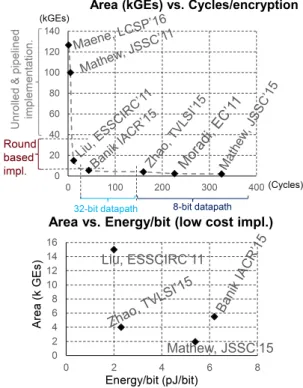
Recently, because of the importance of security, there has been a large number of works on optimizing AES for various purposes. The best current works on optimizing area and power/energy consumption of AES are summa-rized in Fig. 1. For high-speed applications such as optical links or high-speed networks, AES is implemented in hard-ware with the round-based implementation [10] or pipeline architecture [12] or unrolled-round architecture [11]. These kinds of architectures can provide Gb of throughput but they also require high-power consumption, which is not suitable for embedded systems or constrained devices. For example, in [12], Mathew et al. present a two-stage pipeline architec-ture which can provide the throughput of 53 Gb/s with the power consumption of 125 mW. These designs often require more than 15 000 2-input NAND gate equivalences (GEs) to hundreds of thousand GEs. The biggest part in parallel architecture is the S-box. In round-based architecture, there are 16 S-boxes for the encryption path and four S-boxes for the key expansion. In this case, the S-boxes may occupy a half of the total area. Round-based architectures often require ten cycles/encryption, unrolled implementations take from one to five cycles/encryption, while pipeline architectures can
Fig. 1. State of the art AES implementation.
complete the encryption of a block in one cycle after the pipeline is fulfilled.
Most of the designs for low-cost and low-power AES focus on 8-b datapaths. 8-b datapath designs can reduce hardware implementation area significantly with the cost of reducing throughput because they use one [13] or two S-boxes [14], [17]. The theoretical limit of 8-b datapath is 160 cycles/encryption. Extreme small designs, such as in [13] and [17], require more than 200 cycles/encryption. Reduction in size also benefits for low-power feature. The activities in 8-b datapath are reduced because there are only 8 b processed in a clock cycle with the cost of additional registers for MixColumns and additional gates for control logics. The additional registers for MixColumns are needed because MixColumns work on 4-B column data that are available only when the whole column is processed. To achieve medium and high throughput, 8-b datapath architectures have to run at high frequency up to GHz.
The further area reduction for 8-b datapath is done by opti-mizing the S-box. In AES standard, the straightforward imple-mentation of the S-box is to use a LUT. However, LUT-based implementations require large area footprint. Furthermore, AES standard describes AES S-box as arithmetic operation in finite field GF(28) and GF(2): find an inverse of the input value
in GF(28) and followed by an affine transform in GF(2) as specified in the standard [4]. Many works tried to optimize the S-box further by using the tower field which is the decompo-sition of GF(28) into GF(((22)2)2) [18], [19]. This can reduce the area of the S-box to about 290 GEs/S-box, while the LUT-based implementations require at least 400 GEs/S-box. Another decomposition of GF(28) is to use the normal basis of GF((24)2) as in [13]. These methods reduce the size
of the S-box but the unbalanced datapath of the S-boxes introduces more activities. In [20], Bertoni et al. present a method to synthesize the S-box for low power by using decode–switch–encode (DSE) method. This can achieve the lowest power consumption but requires more area than the previous methods.
Another option is to use 32-b datapath. AES algorithm is designed for software implementation in modern computers with 32-b instruction set architectures. Therefore, AES in 32-b datapath has a number of advantages. The number of S-boxes is reduced; instead of 20 S-boxes in round-based architectures, 32-b datapath uses only four S-boxes (in case of sharing the S-box between the encryption path and the key expansion) or eight S-boxes (without sharing). The number of cycles required for one encryption is about 44–54 cycles [19], which is at least four times higher than 8-b architectures. Thirty-two-bit datapath architectures also use less registers than 8-b datapath because the MixColumn step may have data of the whole column in one clock cycle. This opens an opportunity to optimize the architecture further for area, throughput, and power/energy efficiency.
In this paper, we focused on the optimizations for 32-b datapath to achieve extreme low-power and low-energy oper-ations but with much higher throughput when compared with 8-b datapath architectures. This is achieved by multiple opti-mizations. First, the number of needed registers is minimized by using a special structure for loading encryption keys and loading data. Second, the logic is minimized by removing the ShiftRow step, then processing the data by columns after ShiftRows and minimizing the control logic. Third, a low-power S-box is selected with the penalty of area to increase the power consumption efficiency. Finally, a clock gating scheme is proposed for the data storage registers to further minimize the power consumption. Our architecture is implemented using ST FDSOI 28-nm technology, a technology for low-power devices.
III. OURPROPOSEDARCHITECTURE
Our proposed architecture is presented in Fig. 2. The encryption path includes four parts: a state register; four S-boxes; a MixColumn; and an output register which also acts as a temporary register to store intermediate results. The key expansion consists of two key registers and a key transformation module to support all key sizes specified in AES. Our design is a 32-b datapath architecture, which means the input data and the input key are divided into 32-b chunks. Each pair of 32-b data and 32-b key is loaded together. This takes four cycles to load the 128-b key and 128-b data and
XOR them into the state register. For 192-b keys and 256-b keys, after the first 128 b are loaded, the encryption is started while the other bits of the key are continuously loaded to maximize the throughput. There are two feedback paths, one in the key expansion and the other in the encryption path. The state register needs to be updated every four cycles with new 128-b data, while the previously expanded word is sent back to the key registers to generate the new expanded key. The details of the optimizations in our proposed architecture are presented in the next sections.
Fig. 2. Our proposed AES architecture.
A. Thirty-Two-Bit Datapath Optimizations
To reduce area and power consumption in the datapath, we minimized the number of flip-flops and control logics in the datapath by using shift registers with a special organization. Shift registers help simplify loading data and loading key steps. The 32-b of both plaintext and key are loaded at the same time into the state register and the key register by using shift operations. By minimizing the number of flip-flops, we also reduced the number of clock buffers and the power consumption of the clock tree because clock buffers in the clock tree consume a large amount of power. A further opti-mization is to select S-boxes with minimal power dissipation. Fig. 3 shows the organization of our proposed state register. The state register is organized so that after loading the input data and the input key, the encryption is done by shifting the data 32 b in each clock cycle. The state register consists of sixteen 8-b registers (forming a “state matrix”) which are further divided into four 4-stage shift registers. AES standard specifies that ShiftRow is a permutation operation on the rows of the state matrix, while MixColum is an operation on the columns. However, in our design, based on ShiftRow specification, we completely eliminated ShiftRows by select-ing the diagonal of the state matrix (from lower-left corner to upper-right corner). The output of the state register after each shift operation is one column of the state matrix after ShiftRow. This reduces the control logics for the state register, and completely removes the logic for ShiftRow steps. In our datapath, in contrast with 8-b architectures, MixColum is designed as pure combinational logics to reduce the number of flip-flops. Thanks to this structure, the state register’s contents will be updated by next state data which are the contents of the output register concatenated with four last bytes of the round operation every four cycles (or after each round finishes) as described in Fig. 4. Consequently, we saved a 32-b register because we need to store only 3× 4-B temporary data from the encryption path in the output register, while the last 32-b data are written back directly into the state register. The output register is a simple 4× 3-stage shift register to save area and power.
BUI et al.: AES DATAPATH OPTIMIZATION STRATEGIES FOR LOW-POWER LOW-ENERGY MULTISECURITY-LEVEL IOTs APPLICATIONS 3285
Fig. 3. Our proposed state register.
Fig. 4. Our proposed output register.
In between the state register and the output register, there are four S-boxes followed by the MixColums to enable processing 4 B in each clock cycle. The temporary results are stored in the output register. When the encryption finished, the results are written out from the output register. In the 128-b key con-figuration, AES encryption module needs ten rounds, which leads to 40 cycles to finish the encryption for a 128-b block of data. The total number of cycles to encrypt a block in our architecture is 44 cycles. For other key configurations, our architecture needs 52 and 60 cycles to encrypt a data block for 192- and 256-b key modes, respectively.
Clock gating technique is applied on the state register and the output register separately to save the dynamic power consumption. For example, in data loading state, the clock to the output register is disabled to save power because there are no valid data to the output register. Furthermore, when in the inactive state, the output of these registers is not changed, which means that there is no activity in the encryption path. The power estimation results show that even in the highest throughput mode (44 cycles/encryption for 128-b key mode) the applied clock gating technique can save more than 13% of power. Certainly, with smaller throughput the clock gating technique can even save much more power consumption.
B. Substitution Box
The S-box has a big impact on area and power consumption of the AES design. In our architecture, we chose S-box implementation for the lowest power consumption. S-boxes may occupy up to 60% of the total cell area, while they consume about 10%–20% of the total power consumption. The smallest implementation of S-boxes until now is from Canright [18]. Canright S-box demonstrates optimized area (292 gates/S-box) but needs more power/energy consumption
Fig. 5. Our DSE S-Box.
because it creates more activities especially in architectures with eight S-boxes. The most popular and straightforward S-box implementation is the LUT-based S-box. LUT-based S-box is bigger in terms of area (434 gates/S-box) but smaller in power/energy consumption than Canright S-box. The most efficient S-box in terms of power consumption is DSE S-box; however, it occupies a larger area. DSE S-box can be further optimized for power consumption using the structure proposed in [20] and described in Fig. 5. The idea is to use an onehot decoder to convert S-box inputs into onehot representation. The nonlinear operations are done by using wire permutation as in lightweight cryptography algorithms. After that, the S-box output in onehot encoding is converted back into the original field.
DSE S-Box can reduce the power consumption because it minimizes the activity inside the S-box circuit. After decoding state, only one signal changes its value to go to the encoding state. Most of the area lost is because of the size of encoder and decoder circuits. This optimization can leads to 10% power reduction to the whole design. Our synthesized DSE S-box has the size of 466 GEs/S-box that is 7% increase in size in comparison with LUT-based S-Box or 1.6 times the size of the smallest S-boxes. The S-boxes in our design consume only 10% of the total power consumption.
C. Key Expansion Optimizations
The key expansion deploys the same mechanism as in the encryption path with further optimizations for S-boxes and loading data into the key registers for different key sizes. The S-box inputs are masked by constant values when not used to save the dynamic power consumption. The expanded key is calculated on-the-fly and fed back directly to the key registers to save area. Key expansion module consists of two 4×4-stage shift registers, and a key transform module, which includes four S-boxes, and an XOR.
Fig. 6. Key registers.
The structure of the two registers is presented in Fig. 6. For 128-b key mode, only the first shift register is used, the clock signal to the second shift register is disabled to save power. For 192-b key mode, the first shift registers and a half of the second shift register is used, while for 256-b key mode, both shift registers are used. The last expanded word of the key expansion output is sent back into the first key register to continue generating the round key. Depending on the key size, the last word may need to be transformed using RotWord, SubWord, and XOR with RCON, a round constant, before being added with other key words. In 128-b key mode, these three operations are applied to the last word every four clock cycles, while in 192-b key mode and 256-b key mode, they are applied every six and eight clock cycles, respectively. The 256-b key mode needs one additional SubWord in the middle of eight clock cycles. The second key register outputs two different key modes: 192-b key mode and 256-b key mode. In 128-b key mode, the second key register is disabled, while the output of the first key register is selected to XOR
with the output from the key transform module. In 192-b key mode, the second stage in the second key register is chosen; and in 256-b key mode, it is the output of the last stage in the second key register.
The key transform module is shown in Fig. 7. The input of the key transform module is the last word from key registers. Based on the key expansion specification, four S-boxes are used in one cycle among four cycles of a round in 128-b key mode and 256-b key mode while in 192-b key mode; the four S-boxes are used every six cycles. Furthermore, during the loading of the key into the key register, these S-boxes are not used. During the idle time, the inputs to these S-boxes are gated by a mask to save the dynamic power. These S-boxes are enabled for the first cycle of a round for 128- and 256-b keys and every six cycles for 192-b key. After that, they remain inactive. This leads to 30% reduction in power consumption of the S-boxes in the key expansion. RotWord step can be removed because it exchanges the position of bytes in a 32-b signal. The RCON constant can be modeled as a shift register as in [13] but in our architecture, we designed it as a LUT of ten constant values to minimize the number of registers in order to reduce the power consumption and minimize the
Fig. 7. Key transform.
clock network. The XOR of the RCON with the output of the S-boxes after RotWord is minimized by XORing only the necessary bits.
The 32-b output of the key expansion is sent directly to the encryption path to beXORed in the AddRoundKey step. The clock gating technique is also applied in the key expansion to save power consumption. During the idle state, the key register and the S-boxes will not create any activities.
IV. EXPERIMENTALRESULTS
Our proposed architecture and a lightweight cryptography algorithm PRESENT are modeled in VHDL, synthesized using Synopsys DC Compiler, and fully implemented using Cadence Innovus into the test chip SNACk using ST FDSOI 28-nm technology. The maximum target frequency is set to 60 MHz that provides the maximum throughput of 170 and 106 Mb/s for AES encryption core and PRESENT encryption core, respectively. This throughput meets the demand of medium-and high-throughput IoT applications. AES encryption module and PRESENT encryption module are combined into the block cipher module in SNACk test chip for comparison. The power consumption at different corner cases is estimated using the post signoff extraction. The following sections present our power estimation results on SNACk chip and the security eval-uation that we implemented using Synopsys PrimeTime Power.
A. Configuration and Test Environment of SNACk
Fig. 8 shows the interface of the encryption module in the SNACk test chip. It contains the test environment for our proposed AES encryption architecture and also a lightweight cryptography algorithm PRESENT for comparison. It has a 32-b data interface with the possibility of selecting different key sizes and the cipher type between AES encryption core and PRESENT encryption core. AES encryption core supports all the encryption modes specified in AES standard including 128-, 192-, and 256-b keys. PRESENT encryption core with the same interface contains two modes: 80- and 128-b keys. The two designs were implemented using the same technology. The test environment for block cipher module in SNACk chip is presented in Fig. 9. The plaintext and the key are loaded from the host through SPI interface. Inside SNACk chip, there is an SPI decoder with the APB-like interface to write the test data into the correct memories including the configuration reg-isters, the key memory, the plaintext memory, and the reference memory. After loading all necessary data, the encryption test is done by activating the control finite state machine. If the encryption is done correctly, the running signal will toggle.
BUI et al.: AES DATAPATH OPTIMIZATION STRATEGIES FOR LOW-POWER LOW-ENERGY MULTISECURITY-LEVEL IOTs APPLICATIONS 3287
Fig. 8. Block cipher module in SNACk test chip.
Fig. 9. Block cipher module in SNACk test chip.
The encryption process continues running repeatedly until the control finite state machine receives the stop signal through the SPI interface. All the power estimation results in the next section are obtained using this test configuration.
B. Power Estimation Results
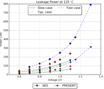
Using the test environment in SNACk chip, it is possible to test two encryption cores with different key lengths at different supply voltages and different operating frequencies. The same key and the plaintexts were sent to each encryption module. The activity of the post signoff timing simulation for each encryption module was captured for the whole encryption period. Then, the activity data were used to do power esti-mation in PrimeTime with FDSOI 28-nm technology libraries provided by ST. The technology libraries were characterized for the supply voltage from 0.6 to 1.3 V for different working conditions. Figs. 10 and 11 show the leakage power and the dynamic power of different encryption modes at 10 MHz with the supply voltage ranging from 0.6 up to 1.3 V at different corners at 125 °C.
It is obvious that the worst case in terms of power consump-tion is the fast corner. Furthermore, it is clear that there are different leakage powers at different corners, while dynamic powers stay unchanged across different corners. The leakage powers increase significantly when we increase the supply voltage especially in the fast corner. Within the same algo-rithm, the leakage power has minor differences for different key sizes; however, the leakage power of AES module is from 2.5 to 3 times the leakage power of PRESENT module. This
Fig. 10. Leakage power at 10 MHz at different supply voltages at different corners.
Fig. 11. Dynamic power at 10 MHz at different supply voltages.
corresponds to the difference in area of two modules. AES module occupies 3.6 times more area than PRESENT module. In terms of dynamic power, because of our optimization for different configuration by using separated clock gating for different key storage, AES module with 128-b key has 20% less dynamic power than AES module with 192- and 256-b keys, while the difference between AES 192- and AES 256-b keys is a small margin. The difference among three corners tested is small. The power consumption decreases gradually when we decrease the supply voltage. The best case in our power estimation results is at 0.6 V where the leakage in different key configuration for the two algorithms is close to each other. At the supply voltage of 0.6 V at typical corner in the worst case of power consumption (at 125 °C), AES module consumes the power from 61.5 to 65.6µW in total and the PRESENT module consumes the power of about 24µW; while in the typical case at 25 °C, our AES module and our PRESENT module consumes only less than 20 and 12 µW, respectively.
TABLE I
COMPARISONWITHOTHERAES IMPLEMENTATIONS
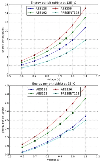
Furthermore, Fig. 12 shows our estimation of energy per bit for two designs. It is clear that our design can achieve extremely low energy per bit at 0.6 V. In typical case at 25 °C, our AES module achieves 0.65, 0.78, and 0.81 pJ/b for 128-, 192-, and 256-b keys, respectively. The energy per bit of different key configurations in AES module varies because different key modes require different number of cycles to finish the encryption. In SNACk test chip, 128-b key AES needs 45 cycles to finish one encryption, 192-b key AES needs 53 cycles, while 256-b key AES needs 61 cycles. The lightweight algorithm PRESENT consumes nearly the same amount of energy per bit as AES because PRESENT needs 74 cycles to finish the encryption of 128-b data in 128-b key mode. In the worst case at 125 °C, our AES consumes less than 3 pJ/b, while PRESENT needs less than 2 pJ/b. The difference in energy per bit in two working conditions is caused by the different leakage power contributed to the total power consumption.
A comparison of our architecture with the state of the art is shown in Fig. 13 and in Table I. From the area point of view, our AES architecture with only 128-b key is 1.5 times bigger than the design in [14] in the same technology node, and four times bigger than the design in [13]. However, our design has four times more throughput than the design in [14] and about eight times more throughput than the design in [13] at the same operating frequency. In comparison with the same 32-b datapath, according to our optimization, our architecture achieve 20% improvement in power consumption in TSMC 65 nm compared with the work in [21] with a small increase in terms of gate counts. At the same throughput of about 28 Mb/s, our architecture consumes the least power (20 µW at 0.6 V) when compared with the 8-b datapath designs such as in [13], [15], and [23]. At this throughput, our proposed architecture has about three times less power consumption than the best 8-b datapath design for low power and low energy in [14]. In terms of energy efficiency, our design consumes the least energy per bit among the low-cost designs [10], [13], [14], [21], [22] with only 0.65 pJ/b (at 0.6 V, 25 °C); and approaches the energy per bit of the high-performance design in [12] (0.511 pJ/b at 409µW, 0.34 V).
Fig. 12. Energy per bit of our AES implementation at typical corner at different working temperatures.
C. Security Evaluation
We also perform correlation power analysis (CPA) attack, one of the most effective side channel attacks, on our design using the last round key hypothesis. The attack is based on
BUI et al.: AES DATAPATH OPTIMIZATION STRATEGIES FOR LOW-POWER LOW-ENERGY MULTISECURITY-LEVEL IOTs APPLICATIONS 3289
Fig. 13. Comparison with other low-cost AES implementations.
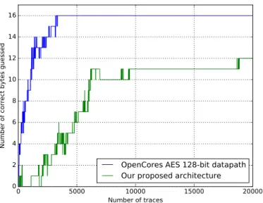
Fig. 14. Number of correct guessed key bytes (in 128-b key mode) by last round CPA attack.
the power trace extracted through the post signoff power estimation. A simulation of 20 000 encryptions of our design in 128-b key encryption mode is executed to capture the ciphertext and the power traces. For comparison, we do the same hardware implementation process with a full parallel design from OpenCores [23]. In general, the more parallel level of the datapath, the harder it is to attack the design because parallelism is one way of hiding countermeasures. 8-b datapath without protection is more exposed to this type of attack because the number of traces required to perform the attack is very small. According to DPA contest [24], even a round-based datapath with full 128-b parallel computation on field-programmable gate array, with good measurement equipment, only 800 traces are required to reveal the key of the cryptographic devices. Fig. 14 presents the results of our experiment on post signoff power traces. The AES 128-b datapath needs about 4000 traces to reveal 16 B of the secrete
key while with our architecture, even with 20 000 traces, only 12 B are revealed. Four bytes are hidden because at the end of each round, the data registers are overridden with new data. This hides the correlation of the activity of the last 4 B of the key which increase the resistance of our design to the last round CPA.
V. CONCLUSION
In this paper, we presented multiple optimization strategies for AES 32-b datapath to achieve a low-cost high-throughput ultralow-power ultralow-energy design with multiple levels of security.
The area of our proposed architecture is saved by a reor-ganization of both datapath and key expansion to minimize the number of registers and control logics. The power con-sumption is reduced by choosing the S-boxes for low power, by minimizing the activity in the key expansion and in the datapath, and by applying a clock gating strategy to data storage registers. The throughput is maximized by using eight S-boxes and doing key expansion in parallel with the encryption path. Multiple key sizes of the encryption module provide different security levels which help IoT applications to adapt to a wider range of security protocols and mechanisms. We also showed that our optimization strategies are not only beneficial for area, throughput, and power/energy con-sumption but also the security feature. With the optimization in the encryption datapath, 32 b of the secrete key cannot be revealed through CPA attacks with 20 000 traces using last round hypotheses. In terms of power and energy consumption, at 0.6 V at 25 °C, our design can achieve a power consumption of less than 20µW for all key configurations with the energy consumption of less than 1 pJ/b with the throughput of 28 Mb/s at 10 MHz. In this condition, our AES implementation has nearly the same energy consumption in comparison with the lightweight cryptography algorithm PRESENT on the same technology node: ST FDSOI 28-nm technology. With high-throughput ultralow-power, ultralow-energy consumption, our design is obviously suitable for future ultralow-power IoT applications.
REFERENCES
[1] R. Roman, P. Najera, and J. Lopez, “Securing the Internet of Things,”
Computer, vol. 44, no. 9, pp. 51–58, Sep. 2011.
[2] A. Barki, A. Bouabdallah, S. Gharout, and J. Traoré, “M2M security: Challenges and solutions,” IEEE Commun. Surveys Tuts., vol. 18, no. 2, pp. 1241–1254, 2nd Quart., 2016.
[3] S. L. Keoh, S. Kumar, and H. Tschofenig, “Securing the Internet of Things: A standardization perspective,” IEEE Internet Things J., vol. 1, no. 3, pp. 265–275, Apr. 2014.
[4] Advanced Encryption Standard, Gaithersburg, MD, USA, U.S Nat. Institute of Standards and Technology, 2001.
[5] IEEE Standard for Local and Mtropolitan Area Networks—Part
15.4: Low-Rate Wireless Persional Area Networks (LR-WPANS),
IEEE Standardization Group, Piscataway, NJ, USA, 2011.
[6] LoraWan Specification, LoRa Alliance, Inc., San Ramon, CA, USA, 2015.
[7] Sigfox. Sigfox Technology Overview—Security, accessed on Nov. 15, 2016. [Online]. Available: https://www.sigfox.com/en/technology/ security
[8] Z-Wave Device Class Specification, Sigma Designs, Milpitas, CA, USA, 2016.
[9] A. Bogdanov et al., “PRESENT: An ultra-lightweight block cipher,” in
Cryptographic Hardware and Embedded Systems—CHES 2007 (Lecture
Notes in Computer Science), vol. 4727, P. Paillier and I. Verbauwhede, Eds. Berlin, Germany: Springer, 2007, pp. 450–466.
[10] P. C. Liu, J. H. Hsiao, H. C. Chang, and C. Y. Lee, “A 2.97 Gb/s DPA-resistant AES engine with self-generated random sequence,” in Proc. Eur. Solid-State Circuit Conf. (ESSCIRC), Sep. 2011, pp. 71–74.
[11] P. Maene and I. Verbauwhede, “Single-cycle implementations of block ciphers,” in Lightweight Cryptography for Security Privacy (Lecture Notes in Computer Science), vol. 9542, T. Güneysu, G. Leander, and A. Moradi, Eds. Cham, Switzerland: Springer, 2016, pp. 131–147. [Online]. Available: https://link.springer.com/chapter/10.1007/978-3-319-29078-2_8
[12] S. Mathew et al., “53 Gbps Native GF(24)2 composite-field AES-encrypt/decrypt accelerator for content-protection in 45 nm high-performance microprocessors,” IEEE J. Solid-State Circuits, vol. 46, no. 4, pp. 767–776, Apr. 2011.
[13] S. Mathew et al., “340 mV—1.1 V, 289 Gbps/W, 2090-gate nanoAES hardware accelerator with area-optimized encrypt/decrypt GF(24)2 poly-nomials in 22 nm tri-gate CMOS,” IEEE J. Solid-State Circuits, vol. 50, no. 4, pp. 1048–1058, Apr. 2015.
[14] W. Zhao, Y. Ha, and M. Alioto, “AES architectures for minimum-energy operation and silicon demonstration in 65 nm with lowest energy per encryption,” in Proc. IEEE Int. Symp. Circuits Syst. (ISCAS), May 2015, pp. 2349–2352.
[15] T. Shirai, K. Shibutani, T. Akishita, S. Moriai, and T. Iwata, “The 128-bit blockcipher CLEFIA,” in Proc. 14th Int. Conf. Fast Softw. Encryption, 2007, pp. 181–195.
[16] Zigbee Alliance. Zigbee Specification, accessed on Aug. 1, 2016. [Online]. Avilable: http://www.zigbee.org/wpcontent/uploads/2014/11/ docs-05-3474-20-0csg-zigbee-specification.pdf
[17] A. Moradi, A. Poschmann, S. Ling, C. Paar, and H. Wang, Pushing
the Limits: A Very Compact and a Threshold Implementation of AES
(Lecture Notes in Computer Science), vol. 6632. Berlin, Germany: Springer, 2011, pp. 69–88.
[18] D. Canright, A Very Compact S-Box for AES (Lecture Notes in Computer Science), vol. 6632. Berlin, Germany: Springer, 2005, pp. 441–455. [19] A. Satoh, S. Morioka, K. Takano, and S. Munetoh, “A compact
rijndael hardware architecture with S-box optimization,” in Advances
in Cryptology—ASIACRYPT (Lecture Notes in Computer Science),
vol. 3659. Berlin, Germany: Springer, 2001, pp. 239–254.
[20] G. Bertoni, M. Macchetti, L. Negri, and P. Fragneto, “Power-efficient ASIC synthesis of cryptographic sboxes,” in Proc. 14th ACM Great
Lakes Symp. (VLSI), vol. 2248. 2004, pp. 277–281.
[21] S. Banik, A. Bogdanov, and F. Regazzoni, “Exploring energy efficiency of lightweight block ciphers,” in Proc. 22nd Int. Conf. Select. Areas
Cryptogr., 2016, pp. 178–194.
[22] Y. Zhang, K. Yang, M. Saligane, D. Blaauw, and D. Sylvester, “A compact 446 Gbps/W AES accelerator for mobile SoC and IoT in 40 nm,” in Proc. IEEE Symp. VLSI Circuits (VLSI-Circuits), Jun. 2016, pp. 1–2.
[23] Opencores. AES128, accessed on Nov. 15, 2016. [Online]. Available: https://opencores.org/project,aes_crypto_core
[24] Telecom ParisTech. Dpa Contest V3, accessed on Nov. 15, 2016. [Online]. Available: http://www.dpacontest.org/v3/
Duy-Hieu Bui (S’13) received the B.Sc. degree in
electronics telecommunication technology from the Vietnam National University-University of Engineer-ing and Technology (VNU-UET), Hanoi, Vietnam, in 2010, and the M.Sc. degree in network and telecommunications from the University of Paris-Sud, Orsay, France, in 2012. He is currently pursuing the Ph.D. degree with the University of Grenoble Alpes, MINATEC Campus, Grenoble, France.
From 2010 to 2015, he was a Researcher with the VNU-Key Laboratory for Smart Integrated Systems, VNU-UET. His current research interests include hardware/software codesign and verification, embedded systems, VLSI system/circuit designs for infor-mation security, and hardware security.
Diego Puschini received the Diploma degree in
elec-tronic engineering from the Universidad Nacional del Sur, Bahia Blanca, Argentina, in 2004, and the Ph.D. degree in microelectronic from Université Montpellier II, Montpellier, France, in 2009.
In 2009, he joined CEA-LETI, MINATEC Cam-pus, Grenoble, France, as a Research Engineer. He has authored or co-authored more than 30 scientific contributions to international conferences, journals, and book chapters concerning power management in distributed architectures. He holds two interna-tional patents. His current research interests include energy-aware design and emergent control techniques for energy management in multicore embedded systems.
Simone Bacles-Min received the M.S. degree in
microelectronics from the Grenoble Polytechnical Institute, Grenoble, France, in 2006.
In 2014, she joined CEA-LETI, Grenoble. Her current research interests include hardware–software codesign and low-power and adaptive security circuit techniques.
Edith Beigné (SM’13) was with CEA-LETI,
Greno-ble, France, in 1998. Since 2009, she has been a Senior Scientist with the Digital and Mixed-Signal Design Laboratory, where she involved in low power and adaptive circuit techniques, exploiting asyn-chronous design, and advanced technology nodes, such as FDSOI 28 and 14 nm, for many differ-ent applications from high-performance MPSoC to ultralow-power Internet of Things applications. She is an SSCS Distinguished Lecturer from 2016 to 2017. She has authored or co-authored more than 100 publications.
Ms. Beigné has been a part of ISSCC TPC since 2014 and VLSI Symposium since 2015.
Xuan-Tu Tran (M’06–SM’13) received the B.Sc.
degree in electronics engineering and communica-tions from the Hanoi University of Science, Hanoi, Vietnam, in 1999, the M.Sc. degree in electron-ics engineering and communications from Vietnam National University (VNU), Hanoi, in 2003, and the Ph.D. degree in micro nano electronics from Grenoble INP (in collaboration with the CEA-LETI), Grenoble, France, in 2008.
He was a Lecturer with VNU from 1999 to 2003. He was a Research Engineer with CEA-LETI, MINATEC, Grenoble, from 2003 to 2008. He was an Invited Professor with the University Paris-Sud, Orsay, France, in 2009 and 2010, and a Visiting Professor with Grenoble INP in 2011. He is currently an Associate Professor with the Faculty of Electronics and Telecommunications, VNU University of Engineering and Technology, Hanoi, and also the Director of VNU-Key Laboratory for Smart Integrated Systems. He is in charge for CoMoSy, VENGME, ReSoNoC, and ADEN4IOT projects for embedded systems and multimedia applications. His current research interests include design and test of systems-on-chips, networks-on-chips, design-for-testability, asynchronous/synchronous VLSI design, low-power techniques, and hardware architectures for multimedia applications.