HAL Id: hal-01745689
https://hal.archives-ouvertes.fr/hal-01745689
Submitted on 16 Jul 2018
HAL is a multi-disciplinary open access
archive for the deposit and dissemination of
sci-entific research documents, whether they are
pub-lished or not. The documents may come from
teaching and research institutions in France or
abroad, or from public or private research centers.
L’archive ouverte pluridisciplinaire HAL, est
destinée au dépôt et à la diffusion de documents
scientifiques de niveau recherche, publiés ou non,
émanant des établissements d’enseignement et de
recherche français ou étrangers, des laboratoires
publics ou privés.
SneakPath compensation circuit for programming and
read operations in RRAM-based CrossPoint
architectures
Alexandre Levisse, Bastien Giraud, Jean-Philippe Noel, Mathieu Moreau,
Jean-Michel Portal
To cite this version:
Alexandre Levisse, Bastien Giraud, Jean-Philippe Noel, Mathieu Moreau, Jean-Michel Portal.
Sneak-Path compensation circuit for programming and read operations in RRAM-based CrossPoint
architec-tures. 2015 15th Non-Volatile Memory Technology Symposium (NVMTS), Oct 2015, Beijing, China.
�10.1109/NVMTS.2015.7457426�. �hal-01745689�
SneakPath Compensation Circuit for Programming
and Read Operations in RRAM-based CrossPoint
Architectures
A.LEVISSE1,B.GIRAUD1,J.P.NOËL1,M.MOREAU2,J.M.PORTAL2
1
Univ. Grenoble Alpes, F-38000 Grenoble, France; CEA, LETI, MINATEC Campus, F-38054 Grenoble, France
2Aix-Marseille Universite, IM2NP, CNRS UMR 7334, F-13453 Marseille, France
Email: [email protected]
Abstract— Passive crossbar memories based on resistive switching bit-cells are today seen as the most promising candidates for flash memories replacement. However, inherent sneak currents through unselected devices lead to low operating margins and over-consumption during read and programing operations. Crossbar memory simulations with bit-cells based on two terminal nonlinear selectors, also show degraded performances due to sneak path currents, leading to nonfunctional memories. Thus, peripheral circuits have to be designed in order to mitigate the sneak currents that impact memory operations. In this paper, we propose a dynamic sneak current compensation circuit for SET and read operations, enabling multi-level cell programming. This circuit is simulated using CMOS 130nm Bulk core process with OxRAM and tunnel barrier-based selector bit-cell.
Keywords—CrossPoint, NonVolatile Memory, RRAM, compensation circuit, Multiple Level Cell.
I. INTRODUCTION
While conventional non-volatile memories (NVM) turn out to be more and more costly and complex to co-integrate with conventional CMOS process, emerging back-end of line resistive switching memories (RRAM) are becoming more and more attractive for high density NVM [1]. Oxide-based RRAM (OxRAM) are one of the most encouraging RRAM technologies due to non-exotic materials, high scalability and fast switching [2]. The conventional 1T1R bit-cell architecture provides good performances but it suffers from a high silicon surface due to access transistor since the bit-cell area has to be as small as possible in order to reduce as maximum the manufacturing cost. In this context, RRAM-based crossbar memories appear to be a promising candidate thanks to an ultra-dense structure (4F²) and 3D stackability [3].
It has been demonstrated that RRAM bit-cell with linear behavior in crossbar memories leads to an unacceptable over-consumption, degraded read performance and limited array size due to inherent sneak currents through unselected RRAM bit-cells (Sneak-Path, SP) [4]. To reduce the SP issues, non-linear RRAM devices have been intensively studied [5]. These linear devices are realized by stacking a RRAM with a non-linear element to form a 1 Selector / 1 RRAM (1S1R) bit-cell, as illustrated in Fig. 1. Different structures of selectors are reported in the literature [6] [7] [8], each having specific
physical and electrical characteristics to mitigate the SP and reduce its impact. The selector purpose is to reach an ultra-low current in the off-state and a steep transition to the on-state with a high current.
To achieve a high-capacity RRAM-based crossbar array, the SP effect has to be reduced as much as possible. To mitigate the SP, polarization schemes are applied on the unselected elements of the array, but they are not sufficient to fully counterbalance its impact on operations. Therefore, a peripheral circuitry has to be designed in order to better compensate the SP effect. Sampling-based SP compensation circuits using Analog-to-Digital converters (ADC) are studied in the literature [9] [10]. The fact that the sampled SP current is compensated using programmable current limitation implies that a large peripheral circuit is needed to ensure a sufficient ADC precision. This approach is performed in 2 steps: firstly the SP is sampled and in a second time, the programing is done.
In this paper, the SP impact on programming operations is studied and a novel SP compensation circuit is proposed. The presented circuit provides immunity to SP, which can be used for Multi-Level Cell (MLC) programming, and also for precise read operation. The SP is dynamically monitored and compensated in order to provide a one-step programming operation. The presented circuit is also studied for use as a sense amplifier on MLC programming operations.
Section II describes the RRAM device model, the selector device and the simulation methodology used in this work. Section III focuses on the proposed circuit during programing operation, whereas Section IV deals with its use for read operations. Finally, Section V draws the conclusions and perspectives.
II. BIT-CELL MODELING AND ARRAY BIASING SCHEME
Two dedicated 1S1R models are considered for simulations: an HfO2/Ti-based bipolar OxRAM compact model calibrated on
silicon data [11] and a Ta2O5/TaOx/TiO2 tunnel barrier-based
selector model [6]. An array of 1S1R bit-cells with post-layout parasitic elements is simulated using Eldo simulator (Fig. 1). Concerning technology, 130nm CMOS Bulk technology from STMicroelectronics is considered.
Fig. 1: Crossbar architecture based on 1S1R cell. The
bit-cell consists of two devices: an HfO2/Ti-based bipolar RRAM
and a Ta2O5/TaOx/TiO2 tunnel barrier-based selector.
During a read or write operation in a crossbar array, SP currents degrade the operation efficiency (read margin reduction and write current control reduction) [12] [13]. Fig. 1 shows the programming current through the selected bit-cell and the SP current through the unselected ones. To overcome this issue, specific wordline (WL) and bitline (BL) polarization schemes are used (Fig. 2). The selected WL (SWL) is polarized at Vselect and the selected BL (SBL) is pulled to the ground. Intermediate voltages (Vselect/2) are applied to unselected WLs (UWL) and BLs (UBL). This commonly used polarization scheme is named ½ bias in the literature [14]. The ½ bias is used in rest of the paper.
Fig. 2: Diagram of crossbar array with detailed polarization
scheme for SP mitigation. This polarization scheme is the best in terms of power efficiency because almost all the array is not concerned with SP [14].
III. SNEAKPATH COMPENSATION CIRCUIT FOR PROGRAMMING OPERATIONS
As described in Fig. 2, the SWL current is the sum of the SP current and the selected bit-cell current. Thus, during a SET operation, current control on the selected bit-cell is hard to reach due to the SP effect [10].
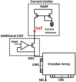
Fig. 3 shows a programing circuit containing two blocks: a simple current mirror and a voltage regulation (Low DropOut Regulator – LDO).
Fig. 3: Schematic diagram of a programming architecture. It
contains a current mirror and a LDO regulator. The LDO part is added in order to maintain the SET voltage on the SWL.
Considering a constant programing current on the SWL, when the array size increases, the programing current decreases as shown in Fig. 4-a. This programming current degradation can be compensated while increasing the current reference value (Iref). However, this approach leads to an increase of programming current variability due to the unselected bit-cell resistance states. Regardless how the Iref compensation is done (compensation on the 50%LRS-50%HRS array as shown Fig. 4-b), it leads to a larger distribution of the programing current. Moreover, it has been demonstrated that lower is the programming current, wider is the programmed resistance values distribution [15]. This shows that the SP has to be considered as a major constraint in the SET circuit conception. Fig. 5 presents the proposed circuit architecture to overcome the SP issues during SET operations.
RRAM Selector 1S1R W or d Li n es BitLines Programming current SneakPath parasitic current WL Rline Vselect Vselect/2 gnd
No SneakPath
Sne akP ath w ith V select /2 SneakPath with Vselect/2 Vselect/2 Vselect/2 Vselect/2 Vselect/2 Vselect/2SWL
SBL
Vset VddH Current reference Additional LDO Current Limiter Crossbar Array SWLIref
UWL UBL SBLFig. 4: (a) Programing current reduction due to SP as a
function of array size. (b) For each array size, the current reference (Iref) is increased to compensate the SP. Compensation can be done using 50%HRS-50%LRS array. In this case, with a low SP current (full HRS array) the programming current is increased. Oppositely, the programming current is reduced in a full LRS array. This leads to an increased variability of the reached resistance.
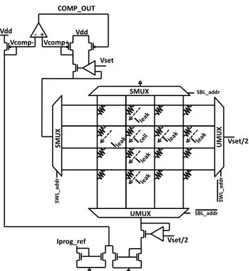
Fig. 5: Schematic diagram of the proposed programing circuit
providing SP immunity with fine SET current tuning. Multiplexers are based on full analog switches; MUX control signals activate only the selected WL and BL in SMUX. Complemented addresses activate all the switches in UMUX except the selected ones.
During a programing phase, UWLs and UBLs are polarized to half of the programing voltage. This polarization scheme limits SP currents to the SWL and SBL. The current provided by the SWL contains two distinct contributions: the programing current (IPROG) and the parasitic current pulled by unselected
BLs (IUBL). Considering IPROG_REF as a current reference
corresponding to the targeted programing current, it is possible to compare IPROG + IUBL to IPROG_REF + IUBL. When it passes over
IPROG_REF, the COMP_OUT signal switches from 0 to VDD. This
process stops the programing operation and limit the current flowing through the selected bit-cell. LDOs are connected to the SWL and UBLs in order to control the voltages applied in the array. The consumed current is measured with current mirrors connected to the LDOs. Currents mirrors can also be cascoded to provide a better current copy. The two currents (IPROG_REF +
IUBL and IPROG + IUBL) are read with the VCOMP+ and V
COMP-signals. These voltages are compared with a differential amplifier.
Simulation results are presented in Fig. 6. We compare the proposed structure (Fig. 5) to circuits shown in Fig. 3. The proposed circuit provides SP immunity and thus a fine control of the programming current.
Fig. 6: Programing current evolution in the selected bit-cell
vs array size (considering a crossbar array with a square form factor). The proposed circuit (Fig. 5) is neither impacted by the array size nor by the resistance state (LRS or HRS) of unselected bit-cells in the array.
IV. SNEAKPATH COMPENSATION CIRCUIT FOR MLCREAD
OPERATIONS
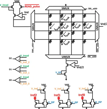
In a large crossbar array and due to SP, reading different resistance level on the same bit-cell can be difficult to operate without increasing significantly the read consumption [16]. The proposed SP compensation circuit can be advantageously used to increase the read precision. This section presents a way to read a MLC bit-cell in crossbar arrays based on the circuit concept presented in Fig. 5.
Fig. 7 presents a one-cycle read circuit based on Fig.5. Several current references (Iref0-2) are added to the SP (IBL) and are compared to the read current (IWL). For a 2 data-bits MLC RRAM, 3 different references are used to read the 4 different resistances states. D<0-2> bits are generated comparing the V_Iread to the 3 references V_Iref_0-2. Fig 8-a shows the resistance distributions obtained with 1000 Monte-Carlo simulations per programming current. CMOS variability and state of the unselected resistances are taken into account in 0µ 50µ 100µ 150µ 200µ 250µ 1 4 16 64 256 1024 Pr og ramming cur ren t [A] Array size [BL] Full HRS Array Full LRS Array 0µ 50µ 100µ 150µ 200µ 250µ 1 4 16 64 256 1024 Pr og ramming cur ren t [A] Array size [BL] a b Full HRS Array Full LRS Array SBL_addr UMUX SBL_addr SMUX SWL _addr SWL _addr SMUX UMUX Iprog_ref Vset/2 Vset/2 Vdd - + Vset Vdd COMP_OUT Vcomp+ Vcomp-0 50 100 150 200 250 1 4 16 64 256 Programmi ng curren t [μA ] Array size [BL] Proposed circuit LDO based circuit Mirror based circuit
100% HRS array 100% LRS array
50%LRS-50%HRS array No impact of the SP resistances
Monte-Carlo simulations. Three distinct LRS and one HRS are visible leading to a 2 data-bits MLC bit-cell. It also shows how the 3 current references are chosen. Fig. 8-b presents the correspondence between the outputs code and the resistance state and Fig. 8-c shows the transient evolution of D<0-2> during a read pulse for resistance state.
Fig. 7: Schematic diagram of the proposed circuit for read MLC
(3 bits) in 1 cycle using ½ bias polarization scheme. The READ_pulse signal activates the selected WL LDO.
Fig. 8: (a) Read current distribution (1000 Monte Carlo
samplings) for the circuit presented in Fig. 5 with detailed choice of the current references. (b) Correspondence table between resistance state and output code (D<0-2>). (c) Transient evolution of D<0-2> during a read pulse.
V. CONCLUSISON
This paper presents a SP compensation circuit to overcome SET and read operation issues in the RRAM-based crossbar memory circuits. SP impact on programming operation precision is detailed and an innovative circuit is proposed to solve this issue. The presented circuit enhance the immunity to SP currents which enables the design of larger arrays (here, with the considered selector, a 256BL array can be designed). For MLC operations, we demonstrated that a SP compensation circuit is mandatory and showed the operation of a 2 data bits bit-cell using the presented circuit. In order to improve read operations, a read circuit, based on the programming compensation circuit and optimized for MLC operation, is proposed. The presented structures opens the way for MLC operation in crosspoint array which is an efficient way to increase the memory density.
VI. RÉFÉRENCES
[1] S.-H. Lee et al., "Scaling trends and challenges of advanced memory technology," in VLSI-TSA, 2014.
[2] A. Benoist et al., "Advanced CMOS Resistive RAM Solution as Embedded Non-Volatile Memory," in IRPS, 2014.
[3] A. Kawahara et al., "An 8 Mb Multi-Layered Cross-Point ReRAM Macro With 443 MB/s Write Throughput," in JSSCC, 2013.
[4] J. Liang et al., "Cross-Point Memory Array Without Cell Selectors-Device Characteristics and Data Storage Pattern Dependencies," in TED, 2010.
[5] A. Chen, "A Comprehensive Crossbar Array Model With Solutions for Line Resistance and Nonlinear Device Characteristics," in TED, 2013. [6] J. Woo et al., "Electrical and Reliability Characteristics of a Scaled
(~30nm) Tunnel Barrier Selector (W/Ta2O5/TaOx/TiO2/TiN) with Excellent Performance (JMAX > 107A/cm2)," in Symposium on VLSI
Technology Digest of Technical Papers, 2014.
[7] J.-J. Huang et al., "Bipolar Nonlinear Ni/TiO2/Ni Selector for 1S1R Crossbar Array Applications," in EDL, 2011.
[8] E. Cha et al., "Nanoscale (~10nm) 3D vertical ReRAM and NbO2 threshold selector with TiN electrode," in IEDM, 2013.
[9] T.-y. Liu et al., "A 130.7-mm 2-Layer 32-Gb ReRAM Memory Device in 24-nm Technology," in JSSCC, 2014.
[10] J.-M. Baek et al., "A Reliable Cross-Point MLC ReRAM with Sneak Current Compensation," in IMW, 2015.
[11] M. Bocquet et al., "Robust compact model for bipolar oxide-based resistive switching memories," in TED, 2014.
[12] J. Zhou et al., "Crossbar RRAM Arrays, Selector Device Requirements During Read Operation," in TED, 2014.
[13] S. Kim et al., "Crossbar RRAM Arrays : Selector Device Requirements During Write Operation," in TED, 2014.
[14] L. Zhang et al., "Selector Design Considerations and Requirements for 1S1R RRAM Crossbar Array," in IMW, 2014.
[15] D. Garbin et al., "Modeling of OxRAM Variability from Low to High Resistance State using a Stochastic Trap Assisted Tunneling-based Resistor Network," in EUROSOI-ULIS, 2015.
[16] S. Lee et al., "Comprehensive Methodology for ReRAM and Selector Design Guideline of Cross-point Array," in IMW, 2015.
Vdd Iref0 Vdd Iref1 Vdd Iref2
V_Iref_2 V_Iref_1 V_Iref_0
V_ISP V_ISP V_ISP SBL_addr UMUX SBL_addr SMUX SWL _addr SWL_ ad dr SMUX UMUX Vrd/2 Vdd Vrd Vrd/2 V_ISP D2 -+ V_Iread V_Iref_2 D1 -+ V_Iread V_Iref_1 D0 -+ V_Iread V_Iref_0 V_Iread READ_pulse VDD GND VDD GND VDD GND VDD GND VDD GND READ Puse 111 011 001 000 STATE HRS LRS1 LRS2 LRS3 CODE 000 001 011 111 b
Iref_0 Iref_1 Iref_2
HRS LRS1 LRS2 LRS3 2 Bits a c Time (s) V olt ag e