RESEARCH OUTPUTS / RÉSULTATS DE RECHERCHE
Author(s) - Auteur(s) :
Publication date - Date de publication :
Permanent link - Permalien :
Rights / License - Licence de droit d’auteur :
Bibliothèque Universitaire Moretus Plantin
Institutional Repository - Research Portal
Dépôt Institutionnel - Portail de la Recherche
researchportal.unamur.be
University of Namur
Light emission, light detection and strain sensing with nanocrystalline graphene
Riaz, Adnan; Pyatkov, Feliks; Alam, Asiful; Dehm, Simone; Felten, Alexandre;
Chakravadhanula, Venkata S K; Flavel, Benjamin S.; Kübel, Christian; Lemmer, Uli; Krupke,
Ralph
Published in: Nanotechnology DOI: 10.1088/0957-4484/26/32/325202 Publication date: 2015 Document VersionPublisher's PDF, also known as Version of record Link to publication
Citation for pulished version (HARVARD):
Riaz, A, Pyatkov, F, Alam, A, Dehm, S, Felten, A, Chakravadhanula, VSK, Flavel, BS, Kübel, C, Lemmer, U & Krupke, R 2015, 'Light emission, light detection and strain sensing with nanocrystalline graphene',
Nanotechnology, vol. 26, no. 32, 325202. https://doi.org/10.1088/0957-4484/26/32/325202
General rights
Copyright and moral rights for the publications made accessible in the public portal are retained by the authors and/or other copyright owners and it is a condition of accessing publications that users recognise and abide by the legal requirements associated with these rights. • Users may download and print one copy of any publication from the public portal for the purpose of private study or research. • You may not further distribute the material or use it for any profit-making activity or commercial gain
• You may freely distribute the URL identifying the publication in the public portal ?
Take down policy
If you believe that this document breaches copyright please contact us providing details, and we will remove access to the work immediately and investigate your claim.
This content has been downloaded from IOPscience. Please scroll down to see the full text.
Download details:
IP Address: 138.48.18.104
This content was downloaded on 27/07/2015 at 06:01
Please note that terms and conditions apply.
Light emission, light detection and strain sensing with nanocrystalline graphene
View the table of contents for this issue, or go to the journal homepage for more 2015 Nanotechnology 26 325202
Light emission, light detection and strain
sensing with nanocrystalline graphene
Adnan Riaz
1,2, Feliks Pyatkov
1,3, Asiful Alam
1,3, Simone Dehm
1,
Alexandre Felten
4, Venkata S K Chakravadhanula
1,6, Benjamin S Flavel
1,
Christian Kübel
1,6,7, Uli Lemmer
2,5and Ralph Krupke
1,31
Institute of Nanotechnology, Karlsruhe Institute of Technology, 76021 Karlsruhe, Germany 2Light Technology Institute, Karlsruhe Institute of Technology, 76021 Karlsruhe, Germany 3
Department of Materials and Earth Sciences, Technische Universität Darmstadt, 64287 Darmstadt, Germany
4
Research Center in Physics of Matter and Radiation, University of Namur, Namur, Belgium 5
Institute of Microstructure Technology, Karlsruhe Institute of Technology, 76021 Karlsruhe, Germany 6
Helmholtz Institute Ulm, 89081 Ulm, Germany 7
Karlsruhe Nano Micro Facility, Karlsruhe Institute of Technology, 76021 Karlsruhe, Germany E-mail:[email protected]
Received 11 March 2015, revised 19 May 2015 Accepted for publication 9 June 2015
Published 24 July 2015 Abstract
Graphene is of increasing interest for optoelectronic applications exploiting light detection, light emission and light modulation. Intrinsically, the light–matter interaction in graphene is of a broadband type. However, by integrating graphene into optical micro-cavities narrow-band light emitters and detectors have also been demonstrated. These devices benefit from the transparency, conductivity and processability of the atomically thin material. To this end, we explore in this work the feasibility of replacing graphene with nanocrystalline graphene, a material which can be grown on dielectric surfaces without catalyst by graphitization of polymericfilms. We have studied the formation of nanocrystalline graphene on various substrates and under different graphitization conditions. The samples were characterized by resistance, optical transmission, Raman and x-ray photoelectron spectroscopy, atomic force microscopy and electron microscopy measurements. The conducting and transparent wafer-scale material with nanometer grain size was also patterned and integrated into devices for studying light–matter interaction. The measurements show that nanocrystalline graphene can be exploited as an incandescent emitter and bolometric detector similar to crystalline graphene. Moreover the material exhibits piezoresistive behavior which makes nanocrystalline graphene interesting for transparent strain sensors.
S Online supplementary data available fromstacks.iop.org/NANO/26/325202/mmedia Keywords: nanocrystalline graphene, light emission, light detection, strain sensing (Somefigures may appear in colour only in the online journal)
1. Introduction
Graphene has been extensively explored over the last decade and many aspects of its unique properties have been revealed and investigated [1]. Besides being a promising transparent, conductive and flexible coating material it is the material’s potential for electronics and optoelectronics which has
attracted a lot of attention [2]. In particular the light–matter interaction in graphene is of interest from a fundamental but also an applications perspective [3]. It has been shown that graphene can be operated as a broadband light detector or emitter and the mechanisms of photocurrent generation and light emission have been revealed as bolometric or electro-thermal and electro-thermal, respectively [4–7]. More recently,
Nanotechnology Nanotechnology 26 (2015) 325202 (10pp) doi:10.1088/0957-4484/26/32/325202
narrow-band light emission and detection have been obtained by photonic engineering through integration into an optical microcavity [8,9]. These devices were based on exfoliated or CVD-grown graphene with domain sizes on the order of micrometers. Thereby manual transfer processing was involved which still poses a challenge for reliable, wrinkle-free wafer-scale device fabrication [10]. Considering the light–matter interactions involved it is however not clear whether graphene with large crystalline domains would be required for operation. Recently the growth of thin carbon films on dielectric surfaces by graphitization of polymeric films has been demonstrated [11, 12]. The simple, metal catalyst-free process yields graphene with nanometer-scale domain size, often referred to as nanocrystalline graphene [13]. Although the low-bias electrical transport of nanocrys-talline graphene is distinctly different from crysnanocrys-talline gra-phene, the material is still conducting and transparent and should be suitable for some of the potential optoelectronic applications [14]. Recently nanocrystalline graphene has been used as the transparent electrode in a silicon photodiode and an organic solar cell [12, 15]. In this work we synthesize, characterize and integrate nanocrystalline graphene into devices, and investigate its feasibility for nanoscale light emission, nanoscale light sensing, and strain sensing. We have studiedfirst the formation of nanocrystalline graphene on various substrates and graphitization conditions, and characterized the material by resistance, optical transmission, atomic force microscopy (AFM), x-ray photoelectron spec-troscopy (XPS), Raman and transmission electron microscopy (TEM) measurements. The conducting and transparent wafer-scale material with nanometer grain size was also patterned and integrated into several devices for studying light–matter interaction and strain sensing.
2. Experimental details
Figure 1 shows the process flow schematically. For the synthesis of nanocrystalline graphene (NCG) we have mod-ified the approach of Zhang and co-workers [11] by spin-coating photoresist onto various substrates and graphitizing the material under high vacuum at high temperatures. As substrates we have used p-doped-Si (〈100〉, boron, ρ < 0.005 Ωcm, thickness 0.381–0.525 mm) with 100 nm, 300 nm and 800 nm thermal oxide from Active Business Company GmbH; n-doped-Si (〈100〉, P, ρ > 1000 Ωcm, thickness 0.525 mm) with 500 nm Si3N4 on top of 800 nm thermal oxide from Active Business Company GmbH; quartz (〈0001〉, z-cut ±0.3°, thickness 0.5 mm) from Alineason Materials & Technology GmbH; and HOQ 310 Quartzglas (thickness 0.5 mm) from Aachener Quarz-Glas Technologie Heinrich GmbH. The lateral dimensions of the substrates were 1 × 1 cm2. The substrates were cleaned for ∼10 s in a sonication bath with acetone, rinsed with Isopropanol (IPA) and dried in a nitrogen stream. Subsequently the substrates were exposed to an oxygen plasma (1 min, 0.2 mbar, 25 sccm O2, 30% power) using an Atto LC PC from Diener electronic GmbH. The clean substrates were then pre-baked for 2 min on
a hot plate at 110 °C. After cool-down, 30μl of photoresist solution was spun onto the substrate under ambient conditions using 8000 rpm for 30 s. The substrates were then soft-baked for 1 min at 110 °C. The photoresist solution was prepared by diluting Microposit S1805 positive photoresist from Rohm&Haas with Propylene Glycol Monomethyl Ether Acetate (PGMEA) of 99% purity from Sigma Aldrich GmbH. PGMEA is the main component of S1805. We have used S1805: PGMEA dilution ratios of 1:14, 1:16, 1:18 and 1:21 to target NCG thicknesses of 6 nm, 4 nm, 2 nm and 1 nm, respectively. The polymerfilms were graphitized by loading them into a Gero Sr-A 70-500/11 high-temperature oven equipped with a quartz glass tube, a turbo-pump vacuum system and a temperature controller unit. After evacuation to ⩽10−6mbar the temperature was raised to 100 °C for∼30 min to promote water desorption. The temperature was then raised to 1000 °C at a rate of 10 °C min−1 and stabilized for 10 h. The samples were cooled down by switching off the heater and were then released to the ambient at temperatures below 100 °C.
Before further processing, the NCG samples were char-acterized by measuring the sheet resistance with the van der Pauw method [16] in a Cascade probe station using gold-plated needles and an Agilent 4155C semiconductor para-meter analyzer. Raman spectra were measured with a Witec CRM 200 confocal microsope under 1 mW laser excitation at 632.8 nm with a Nikon Plan 100x objective (NA = 0.9). X-ray photoelectron spectra (XPS) were measured with an Escalab 250Xi system from Thermo. XPS spectra of the NCGfilms were acquired with a monochromatic AlKα source (1486.6 eV), using a spot size of 400μm and a pass energy of 20 eV. A flood gun was used to prevent charging of the dielectric substrates. Transmission spectra of NCG on quartz were measured in a Cary 500 UV–Vis–NIR spectrometer. Figure 1.Schematic processflow. Substrates were spin-coated with a resist-solvent mixture and graphitized at high-temperature under high-vacuum. The wafer-scale nanocrystalline graphene (NCG) was characterized by Raman spectroscopy, x-ray photoelectron spectroscopy, sheet-resistance measurements and optical transmis-sion spectroscopy. For transmistransmis-sion electron microscopy and diffraction the NCG was transferred onto a grid. Using lithography methods the NCG was patterned for atomic force microscopy and piezoresistivity measurements. Photocurrent and light emission measurements were performed on NCG with electric contacts and a dielectric coating.
For further characterization the NCG samples had to be processed as indicated infigure1. For transmission electron microscopy (TEM) characterization a 2 nm thin NCG layer synthesized on 800 nm-SiO2/Si was transferred onto a Quantifoil holey carbon grid using a direct transfer process [17]. The TEM grid was placed on the sample and a few drops of IPA were added. Due to the hydrophobic nature of both the TEM carbon grid and the NCG, the grid adhered to the NCG layer. The thermal oxide layer was then etched by 2% hydrofluoric acid (HF) overnight. After etching, the TEM grid was rinsed with deionized water (DI) and with IPA. A Zeiss Ultra Plus scanning electron microscope (SEM) was used to confirm the transfer process and to image samples throughout subsequent processing steps. The images were recorded with the in-lens detector at 5 keV beam energy. The high-resolution transmission electron microscopy (HRTEM) images and selected area electron diffraction (SAED) patterns were acquired using an aberration (image) corrected FEI Titan 80–300 operated both at 80 kV and 300 kV acceleration voltage. The electron energy loss spectra (EELS) were recorded at 80 kV. The SAED patterns were processed using the Digital Micrograph (Gatan) script PASAD [18].
For characterizations that required laterally patterned NCG, the samples were locally etched by oxygen plasma. The areas of interest were defined by electron beam (ebeam) lithography and were protected by an aluminum layer. First, tungsten markers were defined by spin-coating 950 k PMMA ebeam resist from Allresist at 5000 rpm for 60 s and baking at 160 °C for 30 min, thus forming a 200 nm thin PMMA layer. The PMMA was exposed by 30 keV electrons using a Raith Elphy Plus pattern processor system attached to a LEO1530 SEM. The exposed PMMA was developed in methyl isobutyl ketone (MIBK) and IPA at a ratio of 1:3 for 35 s. The markers were then formed by sputtering 40 nm tungsten in a Bestec custom design sputtering system (400W DC, 1 min), subse-quently lifted-off in acetone and rinsed with IPA. The NCG was then synthesized by the procedure outlined before. The NCG was then laterally structured with respect to the position of the tungsten markers in a second lithography step by forming, exposing and developing PMMA under conditions identical to the first lithography step. Then 15 nm Al was evaporated as an etch resist. After lift-off in acetone and IPA, the unprotected NCG was etched in an oxygen plasma (3.5 min, 60 mtorr, 20 sccm O2, 30 W) using an Oxford Plasmalab 80 Plus reactive ion etching system (RIE). Sub-sequently the Al resist layer was etched in 3% metal ion-free tetramethylammonium hydroxide (MIF 726) for 30 s. The patterned NCG was then characterized with a Bruker dimension icon atomic force microscope (AFM) in tapping mode to determine the NCG thickness and surface roughness. Piezoresistance measurements of NCG on 800 nm-SiO2/Si were taken in a custom designed three-point bendingfixture with laser-assisted zero-point adjustment. The sample was electrically contacted byfixing flexible Au wires (ϕ = 0.2 mm) using Indium disks (ϕ = 2 mm). The strain induced by extending the central cylindrical post was calculated based on the distance of the cylindricalfixed posts (17.2 mm) and the substrate thickness (0.381 mm), translating into 0.1% strain
per 200μm vertical movement of the central post. Uniform curvature has been assumed.
For photocurrent and incandescence experiments the NCG was electrically contacted and subsequently coated by a dielectric using a third and a fourth lithography step, respectively, by forming, exposing and developing PMMA under conditions identical to the previous lithography steps. The electrical contacts to NCG were made by sputtering 70 nm tungsten and lifting-off in acetone and IPA. A pro-tecting layer of 30 nm Al2O3was formed in a Savannah 100 atomic layer deposition system (ALD) from Cambridge NanoTech, using 273 cycles of alternating 0.02s trimethyl aluminum (TMA) and 0.02s H2O pulses at 200 °C. In a final lithography step using PMMA as etch resist the Al2O3on top of the tungsten contact pads was etched within the RIE (6.5 min, 15 mtorr, 40 sccm Ar + 10 sccm CHF3, 200 W) to ensure good electric contact between probe needles and the tungsten pads. Photocurrent maps have been measured using a NKT SuperK Extreme EXW-6 supercontinuum light source coupled through a NKT SuperK Select acousto-optic tunable filter, a NKT FD-9 fiber, and a reflective beam collimator to a Zeiss Axiotech Vario microscope, equipped with a beam-splitter to guide 90% of the light through a Mitutoyo Plan Apo NIR 100x/0.50 objective onto the sample. The remaining 10% intensity is used for in-situ monitoring of intensity fluctuations during measurement. Samples were mounted on a Standa 8MTF-102LS05 motorized stage (step size: 375 nm) and contacted with probe needles. The backreflected light was measured with a Silicon Sensor PC-50-6 silicon PIN photo-diode, to correlate the photocurrent signal with the sample topography. The photocurrent signal was detected using a Sr 830 lock-in amplifier and a Sr 570 pre-amplifier. The AOTF was used to select the excitation wavelength and the chopping frequency to 1065 nm and 2.3 kHz at 600μW irradiation power. For light emission measurements, a Zeiss AxioTech Vario microscope, directly attached to an Acton Research SpectraPro 2150i spectrometer and a Princeton Instruments PIXIS 256E Silicon CCD camera (1024 × 256 pixels,−60 °C) with in a light-tight box was used. The spectrometer can operate in the imaging mode, with a mirror to take real-space images, or in the spectroscopy mode, with a diffraction grating (300 grooves/mm, 750 nm blaze wavelength). The samples were mounted on a Standa 8MTF-102LS05 motor-ized stage, electrically contacted with probe needles and biased with a Keithley 6430 SourceMeter. Incandescence images and images under external illumination were recorded with a Mitutoyo Plan Apo 80×/0.50 objective.
3. Results and discussion
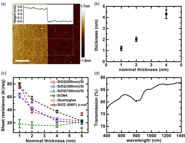
Figure2(a) shows an AFM image across an edge of a structured 1 nm thin NCG layer on 800 nm-SiO2/Si. The data shows that the surface roughness of NCG is similar to the roughness of the SiO2surface, indicating a conformal coating of the substrate. The edge appears straight and shows no sign of underetching. The NCG thickness was adjusted by diluting the resist to yield a targeted nominal thickness. The degree of control is shown in
3
figure2(b). The sheet resistance of the NCG is typically on the order of 20–80 kΩ/sq., depending on the NCG thickness and the type of substrate, as can be seen infigure2(c).
The mean value and the error bars were obtained from measurements on 3–5 samples for each data point. Overall the data shows the expected dependence of the sheet resistance on the inverse layer thickness. The sheet resistance values are comparable to the 30 kΩ/sq. reported by Zhang et al [11] for 1 nm NCG, also formed at 1000 °C albeit under reducing atmosphere. Compared to CVD-graphene [19] and carbon nanosheets [14] the sheet resistance of our NCG is 2 orders of magnitude larger and 2 orders of magnitude smaller, respec-tively. Obviously the carrier transport across grain boundaries has a large influence on the overall resistance. We point out that the graphitization of the resist seems to depend on the surface structure of the SiO2as can be seen by the sensitivity of the sheet resistance to the substrate. Hence the catalytic activity appears to be slightly different for Quartzglass, 〈0001〉 z-cut quartz and 100 nm SiO2 as compared to the thicker thermal oxides on Si. The optical transparency of a
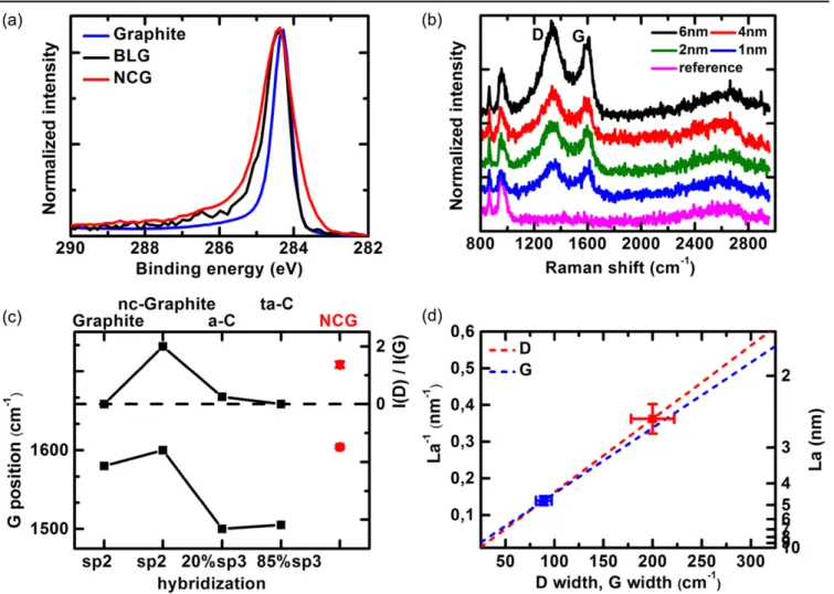
6 nm thick NCG film on 〈0001〉 z-cut quartz is shown in figure2(d). The transmission increases from 77% at 400 nm to 87% at 1400 nm and shows an enhanced absorption around 800 nm. Normalized by the thickness, the optical transmission of NCG is comparable to that of graphene. We speculate whether the enhanced absorption at 800 nm is correlated with the crystallite size and we will come back to this point later in the discussion. To determine the composition and the hybri-dization of the NCG material we have analyzed the C 1s peak of the XPS signal and compared the spectrum to data recor-ded on Bilayer graphene (mechanically exfoliated on 90 nm SiO2/Si) and graphite. Figure3(a) shows that the C 1s signal has a main peak at 284.4 eV similar to graphite, and hence assigned it to the sp2hybridized carbon atoms. Also the width of ∼1.2 eV fits very well to bilayer graphene which has a similar thickness as NCG.
Some peak broadening towards higher and lower binding energy is observed for NCG, which could have its origin in the nanocrystallinity of the material, similar to observations in low-crystalline carbon nanotubes and defective graphite [20,21]. In Figure 2.(a) Atomic force microscopy image of a patterned 1 nm thin NCG layer on 800 nm SiO2/Si substrate. The inset shows an averaged cross-section of the indicated area. Scale bar = 1μm. (b) Measured NCG thickness versus its nominal thickness. (c) Sheet resistance versus nominal thickness of NCG on various substrates as indicated. (d) Transmission spectrum of 6 nm thick NCG on〈0001〉 z-cut quartz. All NCG samples have been synthesized at 1000 °C @ 10 h.
the survey spectrum (not shown), no additional elements besides Si and O from the substrate were detected. Hence we can safely conclude that our NCG is a graphitic material with a high degree of sp2hybridization. XPS also allows determining the thickness of the carbon layer from the attenuation of the photoelectrons emanating from the SiO2[22]. We have used the Si 2p with an attenuation length of 3.5 nm [14] and obtained 0.95 nm for a 1 nm thick layer. Hence the thickness determined by XPS is consistent with the AFM measurement. All samples were characterized by Raman spectroscopy to obtain an addi-tional confirmation on the hybridization and to determine the crystallite size La in the NCG layer. Figure3(b) shows Raman spectra of NCG on 800 nm SiO2/Si for different nominal layer thicknesses. For other process conditions we refer tofigures S1–3. Characteristic to all samples are broad D and G modes, and the absence of a clear 2D peak, similar to [14] and [11]. We used the pioneering work of Ferrari and Robertson to determine the hybridization and crystallinity of our NCG [23]. In figure 3(c) we have compared the G-peak position and the intensity ratio I(D)/I(G) of the D-peak to the G-peak of NCG with the data measured on graphite, nanocrystalline graphite,
diamond-like carbon (DLC) with 20% sp3-content (a-C) and DLC with 85% sp3 (ta-C). The NCG data fits well to the nanocrystalline graphite with 100% sp2 content, and hence confirms nicely the XPS data. From the width of the D and G modes we estimated the size of La by referring to the work of Cançado et al [24]. The D mode width corresponds accordingly to La≈ 4–5 nm, whereas the G mode width indicates La ≈ 2-3 nm. To discern the difference we transferred a 2 nm thick NCG layer formed on 800 nm SiO2/Si onto a TEM grid. The mean value and the spread of the ratio I(D)/I(G), the G-peak position and the width of the D and G modes have been eval-uated from samples prepared on various substrates and of different NCG thicknesses (see table T1 in supporting information).
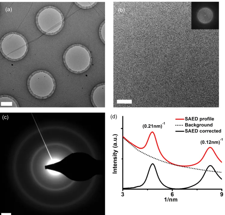
Figures 4(a)–(b) are low- and high-resolution TEM images which show that the NCG film is continuous. Since the morphology appears to be inconsistent with the AFM characterization we assume that the inhomogeneity, visible in figure4(b), is due to residues from the HF etching of SiO2. An SAED image was recorded on a flat region showing continuous diffraction rings (figure4(c)). We were measuring Figure 3.(a) XPS of 1 nm thick NCG layer on 800 nm SiO2/Si, compared with bilayer graphene (BLG) and graphite. (b) Raman spectra of NCG with various thicknesses, grown on 800 nm SiO2/Si. The spectra are normalized to the D-peak and vertically shifted for clarity. (c) Raman G-peak position and intensity ratio of D-peak and G-peak for NCG compared with data [23] for graphite, nanocrystalline graphite and two forms of DLC as explained in the text. The sp-hybridization is indicated. (d) Crystallite size La in NCG determined from the full-width-at-half-maximum of the D- and G-peaks. The dashed lines are extrapolated correlations based on [24]. The graphs (c) and (d) include a statistical evaluation of data from all samples synthesized at 1000 °C.
5
an SAED pattern of a polycrystalline material [25]. The position of the two rings at 0.12 nm−1 and 0.21 nm−1match well to the (110) and (100) reflexes of in-plane oriented graphene, respectively. Although we do not see clear domains in the HRTEM image in figure4(b), the FFT of the image shows nevertheless a lattice plane distance of 0.21 nm−1 (inset, figure 4(b)). A radially averaged line profile of the SAED image is shown infigure4(d), which we have analyzed to determine the average domain size. After background correction we have applied the Scherrer equation to the peak of the (100) reflex with a FWHM of 0.656 nm−1using a shape factor of 0.9 [26]. As a result we obtain an average domain
size of 3 nm, which is closer to the 2.2 nm derived for this film from the width of the Raman D mode peak compared to the G mode width. It should be noted that similar domain sizes of 2–5 nm have been reported by Turchanin et al for organic monolayers graphitized on Au [13]. We have also measured EEELS spectra at the carbon edge of nanocrystal-line graphene (figure S6) and observe transitions which fit to theπ* and σ* states of a graphitic material [27,28].
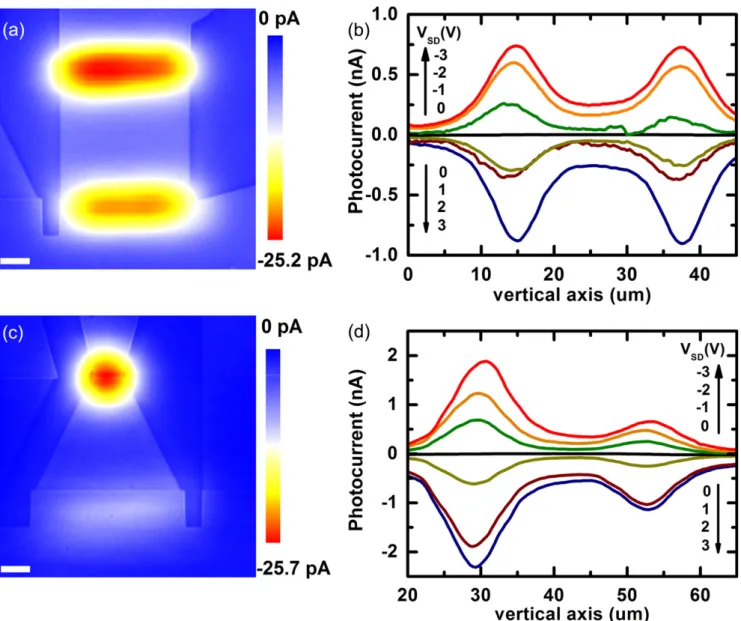
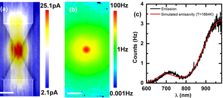
We will now describe the results of the first spatially resolved photocurrent measurements on NCG and discuss the mechanism of photocurrent generation. Figure 5(a) shows a typical photocurrent map of a 20 × 20μm square-shaped NCG Figure 4.Transmission electron microscopy characterization of a 2 nm NCG layer synthesized on 800 nm SiO2/Si in 10 h @ 1000 °C. (a) Low-resolution TEM image of the NCG after transfer onto a holey carbon grid. A fault can be seen in the upper left. Scale bar = 0.4μm. (b) High-resolution TEM image measured through a hole. Scale bar = 4 nm. (c) SAED image. Scale bar = 2 nm−1. (d) Radially averaged line profile of the SAED image.
in contact with tungsten electrodes (overlap 1μm), recorded at +1 V source-drain voltage. We have measured simulta-neously the local reflectivity (not shown) to correlate the photocurrent signal with the sample structure. Instead of superimposing the photocurrent map with the reflectivity map we have superimposed the corresponding SEM image for better visibility of the NCG and adjusted its relative position to the photocurrent map by matching it to the reflectance map (see alsofigure S4). From the data we can see that the pho-tocurrent is generated at the two contacts between NCG and tungsten with similar magnitude. The sign of the photocurrent is phase-shifted by 180° and its magnitude increases with the applied bias. The behavior of the photocurrent is symmetric for both bias polarities as can be seen in the vertical cross-section shown in figure 5(b). Figure 5(c) shows a photo-current map of a 20 × 2μm/20 μm triangular-shaped NCG in contact with W electrodes (overlap 1μm), also recorded at +1 V source-drain bias. In this case the photocurrent is
primarily generated at the contact with the smaller area, where the apex of the NCG triangle is in contact with tungsten. Again the photocurrent is phase-shifted by 180°, the magni-tude increases with the applied bias and the photocurrent is symmetric with respect to the bias polarity (seefigure5(d)). The discussion of the mechanism of photocurrent gen-eration is rather straightforward. The fact that we do not observe a photocurrent signal at zero bias excludes a sig-nificant photovoltaic or electrothermal contribution and can only be explained with a bolometric effect [29]. The tem-perature dependence of the NCG resistance has then to be positive dR/dT > 0 since the photocurrent is phase-shifted by 180° with respect to the applied bias voltage; under illumi-nation the resistance of the sample increases and hence the total current decreases. The photocurrent becomes negative since it is the difference between the total current and the dark current. A bolometric photocurrent must also be correlated with regions of high resistance. Apparently the contact Figure 5.Photocurrent maps of square-shaped (a) and triangle-shaped (c) NCG devices. SEM images were superimposed as explained in the text. VSD= +1 V. Scale bars equal 5μm. (b), (d) Vertical cross-section through the corresponding photocurrent maps as a function of voltage bias. The devices were fabricated from 4 nm thin NCG layers synthesized on 800 nm- SiO2/Si at 10 h @ 1000 °C.
7
resistance between NCG and W infigure5is dominating the total device resistance and hence these regions show up in the photocurrent maps. For asymmetric contacts as infigure5(c) it is only one contact that dominates the entire device resis-tance. Hence bolometric photocurrent mapping can be con-sidered as a tool for mapping the internal device resistance. To test our hypothesis we have patterned within two opposing NCG triangles with 20 × 10μm overall dimensions and a 0.5μm wide and 1 μm long NCG constriction (see also figure S5). As in the previous devices NCG has been contacted with W (overlap 1μm). Figure 6(a) shows that the photocurrent signal is now the highest at the position of the constriction and hence nicely confirms the bolometric picture. We refer also to the photocurrent study of Freitag et al who showed that the bolometric contribution is dominant for the photo-current generation in doped graphene under bias [4]. The responsivity of our device is 1.7 · 10−6A W−1at 1065 nm and hence two orders of magnitude lower than that of graphene [4]. Since the bolometric photocurrent is inversely propor-tional to the squared resistance8, the lower responsivity is likely due to the one order of magnitude higher resistance of our device. We have demonstrated that nanocrystalline gra-phene can be used as a substitute to crystalline gragra-phene for bolometric light detection.
We will now report thefirst study on light emission from nanocrystalline graphene and discuss the mechanism of light generation. Figure 6(b) shows a device with a NCG con-striction under 33 V applied bias voltage and 150μA current. The dimensions of the sample are identical to the one in figure 6(a). We observed a local light emission from the
constriction, which we have identified previously as a region of high resistance (note that a logarithmic intensity scale has been used). As in the case of graphene we anticipate the source of light emission to be thermal radiation [5–7]. We have measured the spectrum of the emission which is shown infigure6(c). The intensity overall increases towards higher wavelength however with obvious modulations. The data could be fitted nicely with a Planck curve and a structure dependent interference term (800 nm SiO2/Si). Details can be found in the supporting information of [30]. We have extracted an electron temperature T = 1664 K. If we assume that the electrical power is mainly dissipated at the NCG constriction we can estimate a local power density p of 1000 kW cm−2. These numbers are very similar to T = 1600 K at p = 520 kW cm−2 reported for graphene [5]. We have therefore demonstrated that nanocrystalline graphene can be used as a substitute to crystalline graphene for generating thermal light emission on the nanoscale with comparable efficiency. Related to our previous work on narrow-band thermal light emission from microcavity-integrated graphene [8], we are currently replacing graphene with NCG to make the entire manufacturing compatible to wafer-scale processing.
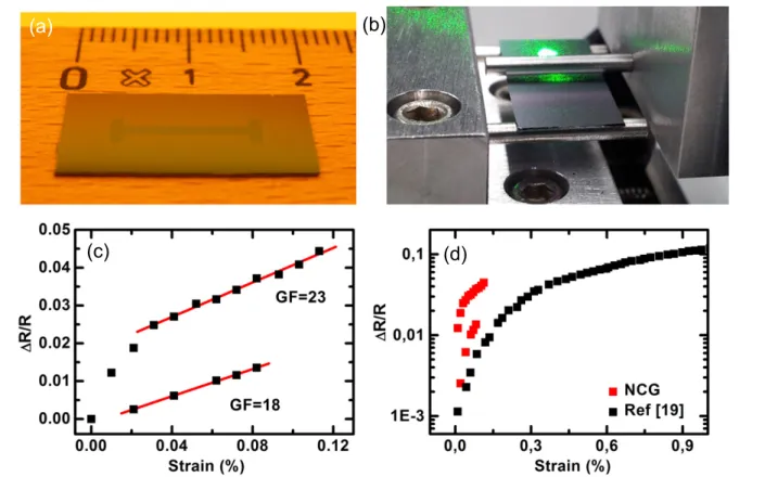
Finally we will discuss a piezoresistive effect that we have been able to measure on nanocrystalline graphene. Figure7(a) shows a sample with a 1 nm thin double T-shaped NCG layer on 800 nm SiO2/Si. The sample was loaded head up into a 3-point bending fixture after electrical wiring (figure7(b)). The resistance had been measured continuously while increasing the strain by vertical displacement of the inner post of thefixture. Data was acquired under increasing strain until sample failure. Figure 7(c) shows the relative resistance change ΔR/R as a function of the strain ε for two samples. The samples show a linear increase ofΔR/R until the breaking of the substrate at ε ≈ 0.1%. The linear slope Figure 6.1 nm thin NCG layer, patterned within two opposing NCG triangles connected by a 0.5μm wide and 1 μm long NCG constriction. (a) Photocurrent map. VSD=−1 V. Scale bar = 5 μm. (b) Light emission image from a contact at VSD= 33 V and ISD= 150μA. Scale bar = 5μm. (c) Emission spectrum recorded at the center of (b).
8
I V R 2( )T R T( T) T;
0 0
Δ = − ⋅ − ⋅ ∂ − ∂ with the bolometric current ΔI, sample resistance R, temperature T and bias voltage V. T0is the temperature
without illumination. The expression has been derived for
[
]
corresponds to the gauge factor and is on the order of 20 for both samples. Whether the linearity continues towards larger strain values is subject to a future study and requires the transfer of NCG onto aflexible substrate. Nevertheless we can compare the data of NCG with measurements on CVD gra-phene as shown in figure7(d). We can see that the relative resistance change is larger in NCG than in graphene at a comparable strain. This obvious difference indicates that grain boundaries play an important role for the appearance of a piezoresistive effect in graphene. Indeed a recent calculation has shown that Klein tunneling should be absent for certain grain boundaries leading to strain-induced conductance modulation [31], which is piezoresistance. If the gauge values continue to be high also at high strain values, then the fab-rication of transparent strain sensors based on NCG can be envisioned, which could offer new functionalities to the emergingfield of transparent and flexible electronics.
4. Summary
We demonstrated the wafer-scale synthesis of nanocrystalline graphene on dielectric surfaces by graphitization of a photo-resist under high vacuum annealing, where the thickness, the sheet resistance and the transparency of the layer was tailored by the process condition. The layer is entirely formed by sp2 -hybridized carbon as proven by XPS and Raman. The size of
the graphitic domains is on the order of 2 nm, consistent with Raman and TEM measurements. Integrated into devices, the material showed photocurrent generation under illumination. The response to light could be traced to a bolometric origin, similar to experiments on doped crystalline graphene. Also light emission under electrical biasing was observed. The emission is due to heating of the layer, and the extracted electron temperature and power density is comparable to experiments reported from crystalline graphene. Furthermore a piezoresistive effect was observed that is significantly larger than in crystalline graphene and indicates the importance of grain boundaries for the appearance of piezoresistivity in graphene. Hence nanocrystalline graphene to appears to be an interesting material not only as an easy-to-fabricate alternative to crystalline graphene for nanoscale light detection and light generation but also towards the fabrication of transparent and flexible strain sensors.
Acknowledgments
RK acknowledges funding by the German Science Founda-tion (INST 163/354-1 FUGG), and RK and AR acknowledge funding by the VolkswagenStiftung. AF is supported by the Belgian fund for scientific research (FNRS).
Figure 7.(a) Optical micrograph of a patterned 1 nm thin NCG layer on 800 nm SiO2/Si suitable for piezoresistance measurements. (b) 3-point bendingfixture with sample inserted head up. The movable piston and the adjustment laser spots are visible; the electrical contacts not. (c) Relative resistance changeΔR/R in NCG versus strain for two samples. The linear fits and corresponding gauge factors are indicated. (d) Comparison betweenΔR/R of NCG with CVD-graphene from [19].
9
Supporting information
Raman data of NCG layers synthesized at different tem-peratures (figure S1), for different graphitization times (figure S2), and on different quartz substrates (figure S3). NCG Raman D and G mode position, width and intensity ratio (table T1). Scanning electron micrograph of laterally pat-terned NCG (figures S4 and S5). EELS spectrum of NCG (figure S6).
References
[1] Geim A K 2009 Graphene: status and prospects Science324
1530–4
[2] Bonaccorso F, Sun Z, Hasan T and Ferrari A C 2010 Graphene photonics and optoelectronics Nat. Photonics4 611–22 [3] Liu M and Zhang X 2013 Silicon photonics: graphene benefits
Nat. Photonics7 851–2
[4] Freitag M, Low T, Xia F and Avouris P 2012
Photoconductivity of biased graphene Nat. Photonics7 53–9 [5] Berciaud S, Han M Y, Mak K F, Brus L E, Kim P and
Heinz T F 2010 Electron and optical phonon temperatures in electrically biased graphene Phys. Rev. Lett.104 227401 [6] Bae M H, Ong Z Y, Estrada D and Pop E 2010 Imaging,
simulation, and electrostatic control of power dissipation in graphene devices Nano Lett.10 4787–93
[7] Freitag M, Chiu H-Y, Steiner M, Perebeinos V and Avouris P 2010 Thermal infrared emission from biased graphene Nat. Nanotechnology5 497–501
[8] Engel M, Steiner M, Lombardo A, Ferrari A C,
Löhneysen H V, Avouris P and Krupke R 2012 light–matter interaction in a microcavity-controlled graphene transistor Nat. Commun.3 906
[9] Furchi M et al 2012 Microcavity-integrated graphene photodetector Nano Lett.12 2773–7
[10] Bonaccorso F, Lombardo A, Hasan T, Sun Z, Colombo L and Ferrari A C 2012 Production and processing of graphene and 2D crystals Mater. Today15 564–89
[11] Zhang Z, Ge B, Guo Y, Tang D, Wang X and Wang F 2013 Catalyst-free growth of nanocrystalline graphene/graphite patterns from photoresist Chem. Commun.49 2789–91 [12] Son S-Y, Noh Y-J, Bok C, Lee S, Kim B G, Na S-I and Joh H-I
2014 One-step synthesis of carbon nanosheets converted from a polycyclic compound and their direct use as transparent electrodes of ITO-free organic solar cells Nanoscale6 678–82
[13] Turchanin A, Weber D, Büenfeld M, Kisielowski C, Fistul M V, Efetov K B, Weimann T, Stosch R, Mayer J and Gölzhäuser A 2011 Conversion of self-assembled
monolayers into nanocrystalline graphene: structure and electric transport ACS Nano5 3896–904
[14] Nottbohm C T, Turchanin A, Beyer A, Stosch R and Gölzhäuser A 2011 Mechanically stacked 1 nm-thick carbon
nanosheets: ultrathin layered materials with tunable optical, chemical, and electrical properties Small7 874–83 [15] Zhang Z, Guo Y, Wang X, Li D, Wang F and Xie S 2014
Direct growth of nanocrystalline graphene/graphite transparent electrodes on Si/SiO 2 for metal-free Schottky junction photodetectors Adv. Funct. Mater.24 835–40 [16] van der Pauw L J 1958 A method of measuring specific
resistivity and Hall effect of discs of arbitrary shape Philips Res. Rep.13 1–9
[17] Regan W, Alem N, Alemán B, Geng B, Girit C, Maserati L, Wang F, Crommie M and Zettl A 2010 A direct transfer of layer-area graphene Appl. Phys. Lett.96 113102
[18] Gammer C, Mangler C, Rentenberger C and Karnthaler H P 2010 Quantitative local profile analysis of nanomaterials by electron diffraction Scr. Mater.63 312–5
[19] Bae S et al 2010 Roll-to-roll production of 30-inch graphene films for transparent electrodes Nat. Nanotechnology5 1–5
[20] Yoon S W, Kim S Y, Park J, Park C J and Lee C J 2005 Electronic structure andfield emission of multiwalled carbon nanotubes depending on growth temperature J. Phys. Chem. B109 20403–6
[21] Barinov A, Malcioǧlu O B, Fabris S, Sun T, Gregoratti L, Dalmiglio M and Kiskinova M 2009 Initial stages of oxidation on graphitic surfaces: photoemission study and density functional theory calculations J. Phys. Chem. C113
9009–13
[22] Laibinis P E, Bain C D and Whitesides G M 1991 Attenuation of photoelectrons in monolayers of n-alkanethiols adsorbed on copper, silver, and gold J. Phys. Chem.95 7017–21 [23] Ferrari A C and Robertson J 2001 Resonant Raman
spectroscopy of disordered, amorphous, and diamondlike carbon Phys. Rev. B64 1–13
[24] Cançado L, Jorio A and Pimenta M 2007 Measuring the absolute Raman cross section of nanographites as a function of laser energy and crystallite size Phys. Rev. B76
064304
[25] Hammond C 1997 Basic Crystallography and Electron Diffraction from Crystals (Oxford: Oxford University Press) [26] Oprea C, Ciupina V and Prodan G 2008 Investigation of
nanocrystals using tem micrographs and electron diffraction technique Rom. J. Phys.53 223–30
[27] Egerton R F 2011 Electron Energy-Loss Spectroscopy in the Electron Microscope (Boston, MA: Springer)
[28] Dasgupta S, Wang D, Kübel C, Hahn H, Baumann T F and Biener J 2014 Dynamic control over electronic transport in 3D bulk nanographene via interfacial charging Adv. Funct. Mater.24 3494–500
[29] Koppens F H L, Mueller T, Avouris P, Ferrari A C, Vitiello M S and Polini M 2014 Photodetectors based on graphene, other two-dimensional materials and hybrid systems Nat. Nanotechnology9 780–93
[30] Khasminskaya S, Pyatkov F, Flavel B S, Pernice W H and Krupke R 2014 Waveguide-integrated light-emitting carbon nanotubes Adv. Mater.26 3465–72
[31] Kumar S B and Guo J 2012 Strain-induced conductance modulation in graphene grain boundary Nano Lett.12
![Figure 1 shows the process fl ow schematically. For the synthesis of nanocrystalline graphene (NCG) we have mod-i fi ed the approach of Zhang and co-workers [11] by spin-coating photoresist onto various substrates and graphitizing the material under high v](https://thumb-eu.123doks.com/thumbv2/123doknet/14511953.721134/4.892.458.825.95.299/schematically-synthesis-nanocrystalline-graphene-approach-photoresist-substrates-graphitizing.webp)