Dynamic ON-resistance in
High Voltage GaN Field-Effect-Transistors
byDonghyun Jin
B.S., Electrical Engineering, Seoul National University, 2008
S.M., Electrical Engineering and Computer Science,
Massachusetts Institute of Technology, 2010
Submitted to the Department of Electrical Engineering and Computer Science in Partial Fulfillment of the Requirements for the Degree of
Doctor of Philosophy
at theMassachusetts Institute of Technology
June, 2014© 2014 Massachusetts Institute of Technology
MASSACHUSETTS ING1TITE OF TECHNOLOGY
JUN 3 0 2014
LIBRARIES
All Rights Reserved.
The author hereby grants to MIT permission to reproduce and distribute publicly paper and electronic copies of this thesis and to grant others the right to so.
Signature redacted
Department of Electrical Engineering and Computer Science
C ertified by _-_ -_____-__-__-___
April 14, 2014
Signature redacted
Jesus A. del Alamo Professor of Electrical Engineering
Accepted by ---
---A
Thesis SupervisorSignature redacted
-u L'slie A. Kolodziejski
Chairman, Department Committee on Graduate Students Author
Dynamic ON-resistance in
High Voltage GaN Field-Effect-Transistors
by Donghyun Jin
Submitted to the Department of Electrical Engineering and Computer Science
April 14, 2014
in Partial Fulfillment of the Requirements for the Degree of Doctor of Philosophy
ABSTRACT
Recently, the development of energy efficient electrical power management systems has received considerable interest due to its potential to realize significant energy savings for the world. With current Si-based power electronics system being matured, GaN Field-Effect-Transistors have emerged as a disruptive technology with great potential that arises from the outstanding material properties of GaN. However, in spite of great progress in GaN device fabrication, electrical reliability and a number of unique anomalies of GaN remain key challenges that prevent the wide deployment of this technology. In particular, the dynamic ON-resistance (RON), in which the RON of the transistor remains high for a certain period of time after a high-voltage OFF-ON switching event, is a critical concern. This phenomenon greatly affects the efficiency of electrical power management circuits based on GaN power transistors. This thesis investigates in depth this important issue.
Firstly, we have developed a new dynamic RON measurement methodology which can observe dynamic RON transients after OFF-to-ON switching events over many decades in time. We have
experimentally demonstrated this technique on GaN-on-SiC high-voltage HEMTs (High-Electron-Mobility-Transistors). The possible origin of the mechanisms responsible for dynamic RON in these
devices has been postulated. Through our new technique, the impact of high-power stress on dynamic
RON has been investigated as well. The results emphasize the importance of studying dynamic RON
characteristics over very short time scale when conducting reliability studies of GaN transistors.
Secondly, high-voltage GaN-on-Si MIS (Metal-Insulator-Semiconductor) HEMTs designed for > 600 V switching operation have been investigated. Excessive electron trapping leading to total current collapse has been observed. We have carried out an extensive characterization of this phenomenon and we have proposed "Zener trapping" as the responsible mechanism. In this view, electron trapping takes place inside the AlGaN/GaN heterostructure through a tunneling process under high-electric-field. The understanding derived here suggests that this effect can be mitigated through attention to defect control during epitaxial growth and appropriate design of the field plate structure of the device.
Our findings in this thesis provide a path to achieve high performance GaN power transistors with minimum dynamic RON effects.
Thesis supervisor: Jesds A. del Alamo Title: Professor of Electrical Engineering
Acknowledgements
I sincerely appreciate my research advisor Prof. Jesds A. del Alamo for his persistent help and great supervision throughout my PhD program. He gave me a great opportunity to work on interesting PhD project and continuously supported me with great intuition and relevant knowledge which are crucial to the success of my research. His high standard of research fostered the depth of this thesis. I greatly benefited from his supervision for my PhD program as well as personal growth toward a professional researcher. I also gratefully acknowledge Prof. David Perreault and Prof. Tomas Palacios for their continuous encouragement and advice which were essential to accomplish my research.
I would like to thank my fantastic mentor Dr. Jungwoo Joh for his generous help and endless advice to my research. He provided me timely answers to all kinds of different questions. I enjoyed all the moments of our technical conversation which often took more than an hour on the phone. His invaluable suggestion helped me in steering our research in directions of greatest relevance to industry. The regular meeting with him plays a significant role to get essential guidance and boost up the research progress. His proactive involvement in our research project helped me to accomplish world-class research in state-of-the-art GaN power switching transistors.
I also would like to show my gratitude toward all the members of del Alamo's Xtreme semiconductor group: Ling Xia, Alex Guo, Shireen Warnock, Luke Guo, Xin Zhao, Wenjie Lu, Yufei Wu, Jianqiang Lin and Alon Vardi. Their strong enthusiasm toward research boosts me up every day and we shared the most of joy, concern and happiness in our daily life. I also would like to thank all my 6th floor
friends. I could spend many precious times together with you guys.
Finally, I owe a debt of gratitude to my parents and my wife, Jae Kyung for their endless love, support and confidence throughout my entire life.
Contents
Chapter 1. Introduction...19
1.1. Introduction to GaN power transistors ... 19
1.2. Motivation: dynamic ON-resistance or current collapse problem...21
1.3. Background ... 23
1.4. Project goal and thesis outline... 25
1.5. References ... 26
Chapter 2. Dynamic ON-resistance in high-voltage GaN-on-SiC HEMTs...30
2.1. Introduction ... 30
2.2. Proposed dynamic ON-resistance measurement technique... 31
2.3. Experimental demonstration on GaN-on-SiC HEMTs... 38
2.4. Im pact of epitaxial growth on dynam ic ON -resistance ... 45
2.5. M echanism s responsible for dynam ic ON -resistance... 50
2.6. Conclusions ... 51
2.7. References ... 52
Chapter 3. Impact of high-power stress on dynamic ON-resistance of high-voltage GaN-on-SiC HEMTs ... 55
3.1. Introduction ... 55
3.2. Experim ents...56
3.4. Conclusions ... 68
3.5. References ... 68
Chapter 4. Total current collapse in high-voltage GaN-on-Si MIS-HEMT ... 71
4.1. Introduction ... 71
4.2. Experim ental set up... 73
4.3. Total current collapse under OFF-state stress ... 75
4.4. Recovery of total current collapse... 77
4.5. Extension and location of current blockage ... 78
4.6. Trapping and detrapping dynam ics ... 83
4.7. Electric field sim ulation ... 88
4.8. M echanism for total current collapse ... 89
4.9. Conclusions ... 93
4.10. References ... 93
Chapter 5. Sum m ary and suggestions ... 95
5.1. Sum m ary ... 95
5.2. Suggestions for mitigating dynamic ON-resistance phenomenon...97
5.3. Suggestions for future research ... 100
List of figures
Figure 1-1. RON transients from 200 ns up to 10,000 s of a virgin GaN transistor when switched from an OFF-state (VGSQ= -5 V, VDsQ= 40 V) to the ON-state switching at room temperature. Blue lines are obtained from pulsed IV system and red lines from semiconductor device analyzer, as described later in this thesis. Also shown are the DC values of RON Obtained after fully detrapping the device. The results show a 52% higher RON at 200 ns than in DC (marked as RONDC). .... ---... 22 Figure 1-2. Device model illustrating the virtual gate effect [26]... 24 Figure 2-1. ID waveform measured by pulsed IV system. The device is synchronously switched from an OFF-state quiescent bias of VGSQ=-10 V, VDSQ=50 V to an ON-state of VGS=l V and VI)s changing from 50 mV to 1.2 V at ambient temperature of 25 'C. Through the simultaneous measurement of both ID(t) and VDS(t) transients in the linear regime, the instantaneous RON(200 ns t 3 ms) is extracted as shown
on th e righ t. ... 32
Figure 2-2. RON transients from 200 ns up to 1,000 s on GaN-on-SiC high voltage HEMTs from an
OFF-state (VGsQ=-5 V, VDSQ=40 V) to ON-state switching at ambient temperature of 55 'C. Blue line is
obtained from pulsed IV system (Auriga AU4750) and red line from semiconductor device analyzer (Agilent B1500A). Also shown is the DC values of RON obtained after fully detrapping the device (marked as RONDC). This shows 66% higher RON at 200 ns than in DC...33 Figure 2-3. Top: VDs and VGS waveforms of three switching events from an OFF state (VGSQ= -5 V, VDsQ= 40 V) to the ON state. In one event, the pulsing is synchronous. In the other two, a delay of 200 ns or 400 ns is introduced between the falling edge of VDs and the rising edge of VGS. Bottom: resulting RON transients are unaffected by the relative alignment of the VDs and VGs pulses indicating that trapping during the transient is negligible. In our relatively small size devices, a fast slew late of 1 V/ns is ob tain ed ... 35
Figure 2-4. Top: RON transients in OFF(VGSQ= -5 V, VDSQ= 40 V) to ON-state switching from pulsed IV in the blue line and from SDA using different OFF-state times of 50, 75, or 100 sec. A visible mismatch occurs with the pulsed IV data. Scaling the SDA-obtained data so as to match ARON(t)IARON(3ms) makes all lines overlap each other as shown in dotted line. The bottom one shows identical normalized RON
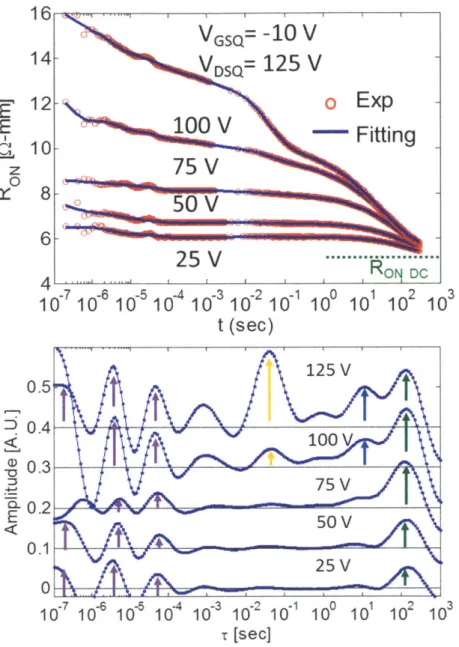
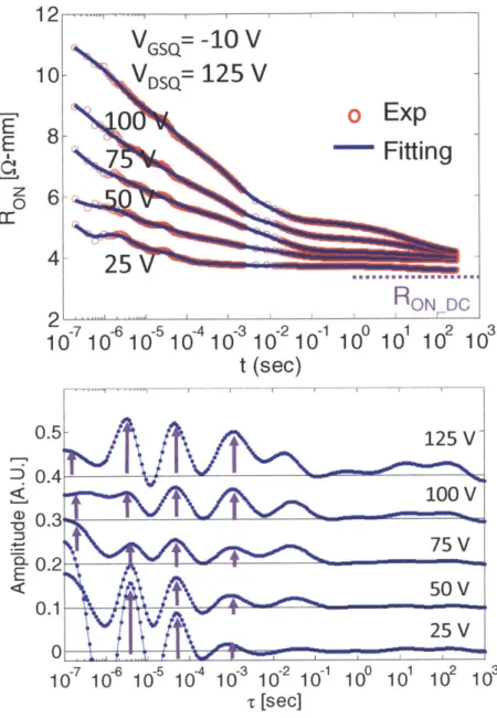
recovery rates suggesting that the RON transients are largely independent of the initial value of RON(3ms). ... 3 7 Figure 2-5. Complete dynamic RON transients from 200 ns up to 10,000 s over 11 decades of time period through our proposed technique in the section 2.2. It has been obtained on GaN-on-SiC high voltage HEMTs from an OFF-state (VGsQ=-5 V, VDSQ=4 0 V) to ON-state switching at ambient temperature of 2 5 C ... 3 8 Figure 2-6. Top: Dynamic RON transients after OFF to ON switching events from different quiescent VDS conditions from VDSQ=2 5 V up to 125 V in 25 V increments at ambient temperature of 25 'C. Red dots are measurements and blues lines are fitting curves through a sum of exponential terms with time constants ranging from 10-s to 103s as shown in the bottom. The device exhibits prominent time
constants in the 10 to 1000 s range and some in the sub-ps to ms range. As VOr increases, the dynamic RON increases too but the time constants do not change... 40
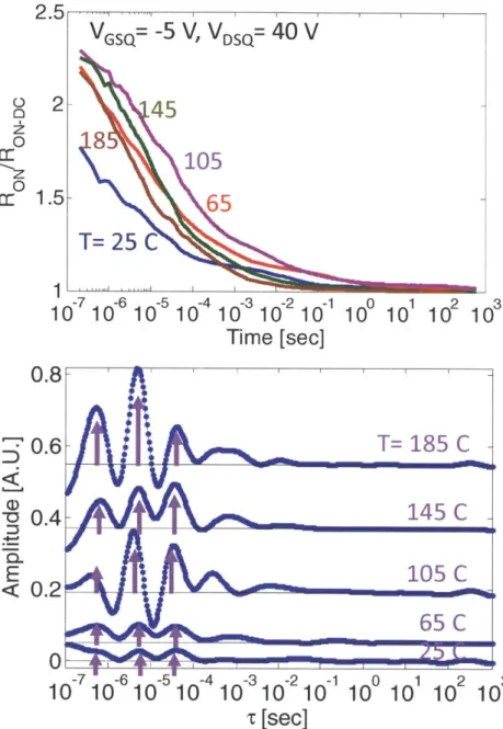
Figure 2-7 Top: RON/RONDC transients at different ambient temperatures for VGSQ=-5 V and VDSQ=40 V.
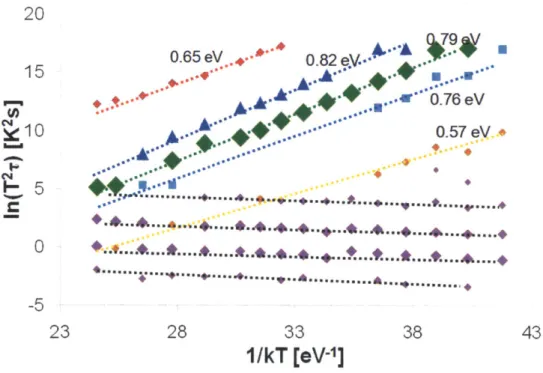
The resulting time constant spectra (bottom) clearly indicate that the dominant transients for long times substantially speed up as the temperature increases whereas short time constants are independent of tem perature...4 1 Figure 2-8. Arrhenius plot of time constant spectrum of Figure 2-7. The size of the symbols is proportional to the height of the time constant peak. Dominant traps at 0.79 eV, 0.82 eV, and 0.76 eV are identified. A set of short time constants which are independent of temperature are also observed. They are responsible for the fast transients...42
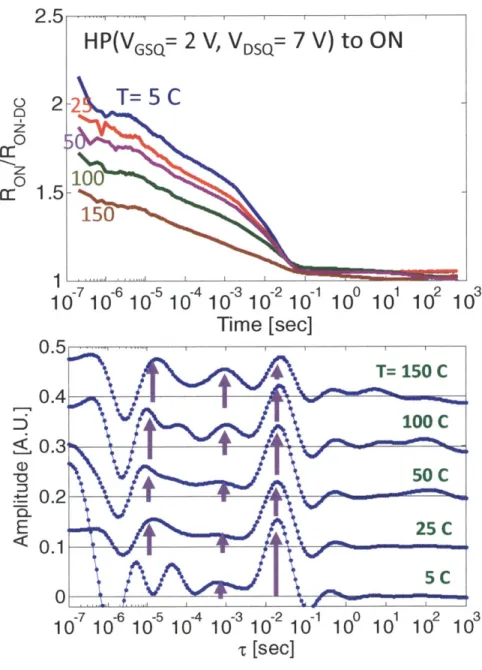
Figure 2-9. High power to ON-state transients at different ambient temperatures and the resulting time constant spectra (inset). The high power state bias is VGsQ=2 V and VDSQ=7 V (the power level was 5.4 W/mm at ambient temperature of 25 0C corresponding to the red line). The transients are dominated by
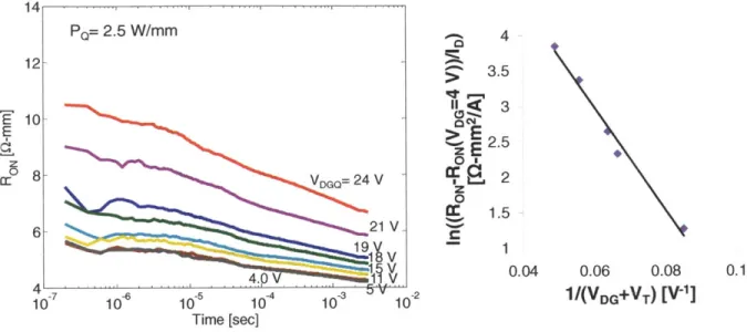
temperature-independent fast time constants. No thermally activated slow-transients are observed. ... 44 Figure 2-10. HP to ON transients from quiescent points at different VDGQ but with the same power dissipation. Dynamic RON at 200 ns increases exponential following a hot-electron type law as shown in
th e righ t. ... 4 5 Figure 2-11. Top: dynamic RON transients in the alternative wafer (see text) after identical OFF to ON
switching events as in Figure 2-6 at ambient temperature of 25 'C. The bottom shows the corresponding time-constant spectra. In contrast to Figure 2-6, devices in this wafer have much weaker time constants in the longer time periods whereas short time constants in the sub-ps to ms range dominate and do not change as V OF increases...47
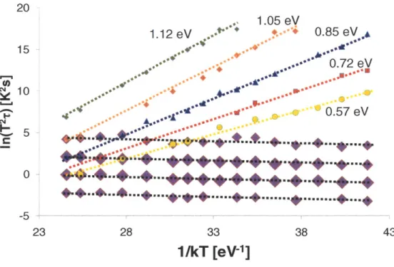
Figure 2-12. Top: RON/RONDC transients in devices from the alternative wafer at different ambient
temperatures for VGSQ=-5 V and VDSQ=4 0 V. The resulting time constant spectra (bottom) show that the dominant transients with short time constants are temperature-independent...48 Figure 2-13. Arrhenius plot of time constant spectrua of Figure 2-12. The size of the symbols is proportional to the height of the time constant peak. A rich spectrum of traps with activation energies between 0.57 eV and 1.12 eV is observed but their concentration is much lower than that in Figure 2-8. The dominant time constants are short and do not exhibit any temperature dependence. ... 49 Figure 2-14. Postulated mechanisms responsible for dynamic RON of GaN HEMTs observed in this work. In the OFF state, electron trapping at the surface, in the AlGaN and at the AlGaN/A1N interface takes place as electrons flow out the gate. In the HP state, hot electrons from the channel are trapped at AlGaN/AIN interface states. In the ON state, electron detrapping takes place thermally for traps in the AlGaN or at the surface and through a tunneling process for AlGaN/AlN interface traps (border traps). .51
Figure 3-1. The operational regions in the RF power amplifier (left) and the power-switching devices (right) are described. The expanded RF load line (left) and the hard-switching operation (right) undergo high-power state continuously which can degrade the device performance. ... 55 Figure 3-2. Time evolution of DC RON, IDMAX (normalized to their initial values) and 1IGOFI during a constant HP-state stress in GaN HEMTs. RON is defined by the inverse of the linear drain current
measured at VGS= 1 V and VDS= 0.5 V and IDMAX is defined at VGS= 2 V and VDS= 8 V. IGOF is the gate leakage current measured at VGs= -5 V and VDS= 0- V. The stress conditions are VGs= 2 V and VDS= 20 V. Up to about 30 min of stress, the device characteristics show minor changes. Beyond 30 min, prominent degradation in both RON and IDMAX and minor one in IGOFFI are observed...57
Figure 3-3. Dynamic RON transients from 200 ns up to 200 s after OFF (VGSQ= -10 V, VDsQ= 50 V) to ON (VGs= 1 V and VDS 1.2 V) switching event in different samples that have been subject to different
HP-state stress periods ranging from 0 to 40 min. Up to 30 min of stress, minor changes in dynamic RON are observed. After 40 min of stress, there is a more than ten-fold increase in dynamic RON. Very fast RON
recovery in the ms range is observed in all cases... 58 Figure 3-4. Normalized dynamic RON (RON/RONDC) of Figure 3-3 at different times (200 ns, 10 ps, and 10 ms) and RONDC/RONDC-virgin (RONDC value in the virgin device) as a function of HP-state stress time in a semilog scale. Dynamic RON mostly increases in a time range from 200 ns up to a few ms. RON_DC/RONDCvirgin shows small increase up to 16% in comparison to dynamic RON suggesting minor perm anent (non-transient) degradation... 59
Figure 3-5. Time-constant spectra for RON transients of Figure 3-3. A sum of exponential terms with time constant ranging from 100 ns to 1000 s is used to fit the measurement data. The equation used for fitting is indicated in the inset. The fit yields the ai coefficient corresponding to each time constant Ti. These data reveal that after 40 min of stress, there is a prominent increase of the magnitude of transients with short tim e constants...60
Figure 3-6. RON/RON.DC transients at different temperatures between 25 'C and 150 0C for VGSQ= -10 V
and VDSQ= 50 V after 40 min HP stress. The inset shows the absolute value of the RON transient. As the temperature goes up, the dominant transients are substantially accelerated. This suggests that the transients are due to generated traps... 61 Figure 3-7. Time-constant spectra for RON transients for temperatures between -55 'C and 150 0C
including the transients in Figure 3-6. Arrows with different colors distinguish individual time constant peaks at different temperatures. Most of them move towards shorter time constants as the temperature increases indicating a thermally activated behavior... 62 Figure 3-8. Arrhenius plot of time constant spectra from Figure 3-7. The size of the symbols is proportional to the height of the time constant peaks and the color of them matches that of the arrows in Figure 3-7. The dominant trap energy levels are located at 0.31, 0.45, 0.53 and 0.57 eV below the conduction band edge most likely in the AlGaN barrier. These are the traps that are responsible for the dramatic increase in dynamic RON that is observed in the short time scale...63 Figure 3-9. Dynamic RON transients after OFF (VGSQ= -10 V, VDSQ= 50 V) to ON switching event for samples subjected to HP-state stress under different conditions. The red solid line indicates a very large increase of dynamic RON up to five-fold RON DC at 200 ns only after 3 min HP stress at VDs= 30 V (P= 9
W/mm). In comparison with the RON/RONDC increase after 20 min HP stress at lower VDS of 20 V and
higher P level of 12 W/mm in pink dashed line, this result suggests that HP stress at higher VDs promotes greater dynamic RON degradation. In all cases, a very fast RON recovery down to the mrs range is observed. ... 6 4 Figure 3-10. Time evolution of normalized DC RON, IDMAX and IGOFF in a constant HP-state stress in devices made from a different epi-supplier sample (denoted as epi-supplier II). The stress conditions are those of Figure 3-2 (VGs= 2 V, VDS= 20 V) but the stress time is extended to 2 hr. In the epi-supplier II sample, there is no prominent permanent degradation in RON, IDMAX and IGOFFI. The large increase of
Figure 3-11. Dynamic RON transient after an OFF (VGSQ= -10 V, VDSQ= 50 V) to ON switching event on epi-supplier II sample before and after 2 hr HP stress at VGS= 2 V and VDs= 20 V (P~- 12 W/mm). In contrast to the large degradation of dynamic RON in epi-supplier I device after the 40 min HP-stress (purple dashed line), there is only a minor increase of dynamic RON observed after 2 hr HP stress in
epi-supplier I sam ple...67
Figure 4-1. Diagram of power device characterization set-up built in the lab. DC and AC stress/characterization can be carried out by Agilent B1505A and Auriga pulsed IV on the Cascade Tesla high-power probe station. Pulsed UV light source system is developed to test detrapping effect depending on light illumination with different wavelength. Automatic computer control environment for each instrument has been developed as well. High voltage test functionality up to 3000V is established from the entire set-up . ... 73 Figure 4-2. Pulsed UV light source system consisting of Xenon fiber optic light source, computer controllable monochromator, and automated filter wheel. The brief functional description per each one is scripted. The UV optical fiber tip drawing the output of light source system is placed closely to the sample on the probe station, as shown on the right, so as to beam UV light directly onto the top of the sam p le ... 7 4 Figure 4-3 (a) Three field plate structures (FP1, FP2, and FP3) placed in a stairway fashion along the gate-to-drain gap in AlGaN/GaN MIS-HEMTs. (b) The waveform of VDS and VGS in the OFF-state step-stress experiment. VDS continually steps up while VGS is biased at VT - 5 V. Every stress period is 10 s. Between each step, IDun which is defined at VGS= 0 V, VDS= 0.2 V is periodically monitored. IDlin is inversely proportional to RON--.---... 75
Figure 4-4. Evolution of normalized IDin in an OFF-state step-stress experiment. VGS is biased at VT- 5 V and VDS is step-stressed by 20 V every 10 seconds up to 720 V. Total current collapse occurs for
Figure 4-5. Six consecutive OFF-state step-stress experiments up to 400 V on the same sample. Detrapping procedure with UV exposer and thermal treatment (180 min at 200'C) has been applied in between each run. Total current collapse characteristic shows complete recovery and repeatability after detrapping procedures suggesting that this results from completely trapping. ... 78 Figure 4-6. Output characteristics before (blue) and after (red) 300 sec of OFF-state stress at VDSSTRESS=
300 V and VGS= VT - 5 V. After stress, at low VDS, nearly complete current collapse is observed.
However, as VDS increases the drain current starts flowing again. The collapsed output characteristics resem ble a punchthrough device ... ...79 Figure 4-7. Evolution of the linear subthreshold characteristics (VDS= 0.25 V) during the stress of Figure
4-3. VTO is the initial threshold voltage where D is 1 -A/mm.VT does not change at all under total current co llap se ... 7 9 Figure 4-8. Evolution of source (Is), gate (IG), drain (ID), and substrate (IB) currents during the stress
periods of Figure 4-5 up to 400 V. As the OFF-state bias increases beyond 300 V, the drain-to-substrate current increases. At the onset of severe trapping, all currents are negligible. ... 80 Figure 4-9. Impact of device geometry on IDun degradation under OFF-state step-stress up to VDSSTRESS= 400 V and VGS= VT - 5 V. The trapping characteristics do not depend on gate-to-drain gap length (LGD), 1st field plate length (Lmpj), 2nd field plate length (L-p2) and 3rd field plate length (LFP3). ... 81
Figure 4-10. Normalized drain-to-gate capacitance (CDG) in the OFF state as a function of VDS. The three steps in CDG indicate the complete extension of the depletion region under each of the three field plates by
VDS= 50 V. For VDS > 50 V, electric field peaks in the channel under the edge of FP3 and where VDS is around 200 V, excessive trapping occurs along this highly localized region and can form very short current blockage region under the edge of FP3 as shown in the cartoon on the right...82 Figure 4-11. (a) Evolution of IDun in OFF-state step-stress experiment at temperatures from 25 to 200 'C. The trapping characteristics are insensitive to temperature. (b) Evolution of drain (ID), source (Is), gate
(IG), and substrate (IB) currents at different temperatures. The terminal currents are not the main source of
electron trapping...84
Figure 4-12. (a) Evolution of normalized IDun as a function of time in a device under constant stress bias from VDS-STRESS=140 to 180 V at room temperature. A characteristic trapping time (r) is defined at the 50% degradation point of IDlin- (b) Zener dependence of T: T vs. 1/EPEAK in a semi-log scale. EPEAK is the peak
value of electric field inside AlGaN layer under FP3 estimated from field simulations in the same OFF-state bias conditions (Figure 4-13). The straight line that is obtained strongly suggests a Zener tunneling process. A trap energy level of around 1 eV above valence band edge is estimated. ... 85 Figure 4-13. Normalized IDun recovery transients in the dark after 600 sec OFF-state stress at VDSSTRESS=
200 V and VGS= VT - 5 V at different temperatures. IDlinDC is the virgin DC value of IDin- As T increases, the recovery speeds up. An activation energy of around 0.63 eV is extracted...87 Figure 4-14. UV-induced recovery of a device collapsed after 300 V OFF-state stress for 3 min for different energies of UV light at room temperature. Enhanced recovery is observed for light energies
above 2 .8 eV ... 87 Figure 4-15. (a) Evolution of electric field at the top surface of AlGaN barrier from gate to drain obtained from TCAD simulations (Silvaco). Beyond VDs=200 V, the peak electric field appears under the edge of the outermost field plate and increases with VDS. (b) Magnitude of EPEAK under third field-plate edge vs. VDS is described. At VDs= 200 V, EPEAK is around 3.4 MV/cm and it increases up to 6.4 MV/cm at 1,000 V ... 8 8 Figure 4-16. Proposed Zener trapping mechanism responsible for the observed total current collapse. Direct electron tunneling from the valence band into defect states can be triggered under intense electric-field inside the AlGaN barrier layer or at the top of the GaN channel...90 Figure 4-17. Energy band diagram along surface from gate to drain with device biased in the linear regime after a total current collapse event. OFF-state trapping results in a sharp energy barrier directly below the edge of the outermost field plate that blocks current. In the linear regime, thermal detrapping
can take place as indicated with an activation energy substantially lower than the ionization energy of the trap ... 90 Figure 4-18. Energy location of traps responsible for Zener trapping. From Zener trapping calculations, ET - Ev = 1.0 eV is extracted and from UV detrapping experiments, Eh, = 2.8 eV is estimated...91 Figure 4-19. Evolution of IDun under VDS=O V condition as VGS steps from -12 V to -48 V with 1 V/step every 30 sec at room temperature. Sharp current collapse is observed as well. In this case, the channel blockage occurs under the source end of the gate. Thermal acceleration behavior in this source-side recovery is clearly observed with an activation energy of 0.50 eV, as shown on the right...92
Chapter 1. Introduction
1.1.
Introduction to GaN power transistors
In our contemporary society, the standard of living has substantially improved but this indispensably requires continuous increase of energy consumption all over the world. However, additional constructions of conventional power plant for the increasing energy demand confront negative social pressure due to their externality to global warming effect. As a result, a tremendous interest has been given to the development of energy efficient electrical power management systems along with high expectations for significant energy saving on a world-wide scale.
The current power management system which controls or transforms electrical energy into different power range with diverse power load such as industrial infrastructures, consumer appliances, automotive applications, and electricity grid system has been developed through Si-based power transistor technology in the last 60 years. In the 1950s, Si bipolar power transistors and thyristors were first invented and in 1980s, insulated gate devices were introduced [1]. Until now, various innovative technical improvements have been introduced through Si-based power transistor technology but nowadays their progress has slowed down as it becomes a matured technology. In the last few years, a great deal of attention has been given to new power transistor technologies based on new material systems. Recently
Gallium Nitride (GaN) power transistors have emerged as a disruptive technology with great potential that arises from the outstanding material properties of GaN [2][3].
The wide band gap (3.4 eV) of GaN, compared to 1.12 eV of Si which dominates commercialized power semiconductors technology today, provides several benefits in future power electronic applications. Firstly, GaN can have a very high critical electric field, about ten times higher than Si [4], which enables
achieving a much higher breakdown voltage in GaN power-switching transistors [5]. Secondly, GaN can have smaller intrinsic carrier densities than Si at the same temperature which provides proper electronic functionality at ambient temperatures higher than 150 'C without external cooling. This is impossible in Si technology due to substantial increase of leakage currents [6]. This also guarantees a much higher thermal limit to power device operation. Moreover, GaN is a compound semiconductor including elements from column three in the periodic table and nitrogen. It is relatively easy to form heterostructures such as AlGaN/GaN which is the most famous one. This can induce a very high sheet electron density in the GaN channel layer of more than 1013 cm-2
through spontaneous and piezoelectric polarization charges without any external doping [7]. In addition, high electron saturation velocity (2.5x 107 cm/s) with high electron mobility (> 1000 cm2/Vs) in the AlGaN/GaN heterostructure is attainable and this provides very high frequency of operation as well [8]. The combination of these superior properties promise better than three orders of magnitude improvement in the ON-resistance/breakdown-voltage trade-off over conventional Si power switching devices [1].
As a result of these outstanding technical attributes, GaN transistors exhibit a significant advantage in terms of size when compared to advanced Si power transistors. In addition, GaN heterostructures can be grown onto wide area Si wafers [9] which enables the fabrication of GaN power transistors in Si fabrication facilities. This mitigates the need for large investment in the creation of new processing infrastructure. The combination of smaller device footprint and GaN-on-Si epi-growth technology might make this technology cost competitive with Si [9].
As a result of the outstanding material properties and expected cost benefits of GaN power transistor technology, intense research efforts are under way around the world. The great progress in device performance has been achieved through diverse approaches using novel device fabrication technologies [10]-[13] and demonstrated greater performance over Si power transistor technology. However, in spite of recent progress in GaN device fabrication technology, a comparative study of reliability is also required but there is not enough understanding today to carry out this critical inquiry. Especially, electrical reliability as well as some unique anomalies of GaN still remain key challenges that prevent the wide deployment of this technology. There are very few studies about the dominant failure mechanisms of GaN power transistors. Significant improvement in reliability is frequently emphasized as a final key hurdle to overcome for commercialization of this technology to become a reality[14][15].
1.2. Motivation: dynamic ON-resistance or current collapse problem
From the wide investigation in the past about the degradation mechanisms of RF power GaN High-Electron-Mobility Transistors (HEMTs) [13],[14],[18],19], similar phenomena are considered to be relevant in GaN power transistors as well. Among several degradation mechanisms and operational anomalies suggested from the studies on those devices, a particular concern is the so-called dynamic ON-resistance (RON) or current collapse problem [20]. Strictly speaking, this is not a reliability problem but in order for GaN power switching-devices to outperform current Si power transistor technology this significant anomaly needs to be resolved.
OFF(-5 V, 40 V) to ON
5.5
Pulsed-IV
Semiconductor
Device Analyzer
5-E
E
c
4.5-0cI
4-5RONc=
3.5
Q
mm
--
-
---
-10
11010 31071010 10 102 103 10
Time [sec]
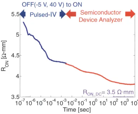
Figure 1-1. RON transients from 200 ns up to 10,000 s of a virgin GaN transistor when switched from an OFF-state (VGSQ= -5 V, VDsQ= 40 V) to the ON-state switching at room temperature. Blue lines are obtained from pulsed IV system and red lines from semiconductor device analyzer, as described later in this thesis. Also shown are the DC values of RON obtained after fully detrapping the device. The results show a 52% higher RON at 200 ns than in DC (marked as RONDC).
Dynamic RON or current collapse refers to a condition in which after an OFF-ON switching event,
RON of the transistor remains high for a certain period of time. The observation of temporary high values of RON as a result of prominent electron trapping that occurs during the off state has been widely reported [21]. Our recent studies have shown that dynamic RON in high-voltage GaN FETs can be very severe with short-time scale RON values that are several times higher than RONDC which is the initial DC value of RON
[12]. The high dynamic RON values can take many hours to fully dissipate at room temperature, as shown in Figure 1-1. The problem also worsens as the OFF-state voltage increases [22]. Dynamic RON is also activated by hot-electron trapping under high-power conditions that might appear during hard switching
[23], [24]. Understanding and solving this problem will require identifying the sources of the traps that are responsible and eliminating them.
Our goal is to achieve fundamental understanding on this problem by developing an appropriate measurement methodology and carrying out systematic characterization of devices with various designs. In addition, we wish to explore any degradation from the impact of various electrical stresses which can be driven by power device operation such as high electric field stress from high blocking voltage in the OFF-state condition or high-power stress during hard switching condition. The impact from special device features such as multiple field plate technology on dynamic RON under electrical stress will also be explored and the dominant mechanisms will be clarified.
1.3. Background
In this section, previous studies about this dynamic RON or current collapse phenomenon are
briefly introduced. An increase of RON or a collapse of drain current that depends on the operational device history is related to the change density in the inversion layer of the AlGaN/GaN heterostructure. The high density of 2 dimensional electron-gas (2DEG) attainable in this heterostructure not only results from spontaneous and piezoelectric polarization effects [7] but also from the existence of a positive sheet of charge at the top AlGaN surface which mostly arises from ionized donor states at the surface [25]. Initial studies about current collapse observed in AlGaN/GaN HEMTs claim that in the high voltage bias condition, the accumulation of negative charge mostly through the injecting electrons from gate electrode into the top AlGaN surface layer induces a reverse biased virtual gate effect [26]. As shown in Figure 1-2, in the reverse bias condition between gate and drain electrodes, incoming electrons are captured by the surface states and neutralize the positive donor states. This results in an extension of the depletion region. In the following ON-state condition, they are usually released with relatively long time constants on the
order of seconds [20] and the 2DEG density along the neutralized surface region is reduced significantly causing the dynamic RON or current collapse during high frequency operation of these devices.
Virtual Gate
++
Drain
- - - - -
- - -- -- -- - - -- -
V V
AIGaN
VVG
G
aN
VG
Source
Extended depletion region
Figure 1-2. Device model illustrating the virtual gate effect [26]
In order to mitigate this virtual gate effect, surface passivation technology has been utilized [27] using mostly SiN passivation layer [28]-[30]. There are reports of surface passivation strongly mitigating current collapse by reducing the surface electric field and preventing the electron injection from the gate electrode into the adjacent surface states [31]. Nowadays, surface passivation is regarded as an essential technology which mostly determines trapping related current collapse phenomenon as well as some device reliability issues.
Another mechanism responsible for current collapse is channel hot electron trapping under high drain voltage operation in the ON-state [24]. In the high voltage and ON-state operating condition, electrons flowing in the channel can obtain very high kinetic energy which enables them to overflow the energy barrier between the AlGaN barrier and GaN channel layer and get trapped at surface states or traps inside the barrier layer [32]. This can also cause a virtual gate effect and perhaps also permanent degradation by trap formation resulting in current collapse [33].
Recently, crystallographic defect formation through the inverse piezoelectric effect has been proposed as a new degradation mechanisms and can induce the current collapse effect as well [34]. Under high electric field condition, the AlGaN/GaN heterostructure can get additional mechanical stress through the inverse piezoelectric effect. If the induced total elastic energy density exceeds a critical value, crystallographic defects such as pits and cracks can be formed. These defects can become trapping sites for electrons and all relevant trapping effects discussed above can become magnified.
1.4. Project goal and thesis outline
Previous studies about dynamic RON or current collapse have been mostly limited to simple
characterization and they fail to contribute detailed understanding. Systematic studies on this problem have not been reported and consensus about the detailed physical origin is still lacking. In addition, systematic studies have yet to be performed in GaN power-switching devices. In our thesis, we target an initial rigorous investigation of this important issue. We will carry out extensive experiments under a variety of stress conditions in devices with various geometries. There can be significant degradation of the dynamic characteristics of GaN FETs as a result of prolonged electrical stress. The importance of electrical reliability studies on transient characteristics, and not just DC characteristics, is emphasized. The effectiveness of multi-field plate design in the industrially prototyped power switching device structures studied here is investigated in detail. Lastly, theoretical degradation mechanism models are presented.
This thesis is organized as follows. In chapter 2, we propose a new dynamic RON measurement methodology which can observe RON transients after OFF-to-ON switching event over many decades of time. Experimental demonstration of this technique on GaN-on-SiC high-voltage HEMTs is presented. Impact of epitaxial growth on dynamic RON is also discussed in. Finally, relevant mechanisms responsible for the dynamic RON observed in GaN-on-SiC HEMTs are proposed.
In chapter 3, by using the newly proposed technique introduced in chapter 2, the impact of high-power stress on dynamic RON characteristics of high-voltage GaN-on-SiC HEMTs is studied. Here, severe degradation of dynamic RON characteristics due to the induced creation of traps with relatively short time constants is discussed in detail. The results emphasize the importance of characterizing dynamic RON or
current collapse characteristics over a very short time scale in electrical stress experiments.
In chapter 4, the current collapse phenomenon in high-voltage GaN-on-Si MIS (Metal-Insulator-Semiconductor) HEMTs designed for > 600 V operation is investigated. Device structures featuring multiple field plate structures and a gate dielectric which are different from the device studied in the previous chapters are discussed in detail. In order to handle the very high operational voltage of this device along with monitoring the current collapse precisely, a unique automatic characterization/stress measurement environment has been developed. From electrical stress experiments in the OFF-state, we have observed trapping that is so severe that leads to total current collapse such that the device effectively behaves as an "open" when subsequently biased in the ON-state. The recoverability and repeatability of this phenomenon and the impact of device geometry and temperature have been investigated in great detail. Based on many experiments, we postulate a responsible mechanism which consists of electron trapping inside the AlGaN/GaN heterostructure that takes place through a tunneling process under high-electric-field.
Finally, in chapter 5 the conclusions and suggestions from our research are presented. Ways to mitigate dynamic ON-resistance phenomenon are suggested. We also propose suggestions for future work.
1.5. References
[1] B. J. Baliga, M. S. Adler, P. V. Gray, R. P. love, and N. Zommer, "The insulated gate rectifier (IGR): A new power switching device," in Electron Devices Meeting, 1982 International, 1982, vol. 28, pp. 264-267.
[2] B. J. Baliga, "Gallium nitride devices for power electronic applications," Semicond. Sci. Technol., vol. 28, no. 7, p. 074011, Jul. 2013.
[3] L. F. Eastman and U. K. Mishra, "The toughest transistor yet [GaN transistors]," IEEE Spectr., vol.
39,no.5,pp.28-33,2002.
[4] R. S. Pengelly, S. M. Wood, J. W. Milligan, S. T. Sheppard, and W. L. Pribble, "A Review of GaN
on SiC High Electron-Mobility Power Transistors and MMICs," IEEE Trans. Microw. Theory Tech.,
vol. 60, no. 6, pp. 1764-1783, 2012.
[5] W. Saito, Y. Takada, M. Kuraguchi, K. Tsuda, I. Omura, T. Ogura, and H. Ohashi, "High breakdown voltage AlGaN-GaN power-HEMT design and high current density switching behavior," IEEE Trans.
Electron Devices, vol. 50, no. 12, pp. 2528-2531, 2003.
[6] P. G. Neudeck, R. S. Okojie, and L.-Y. Chen, "High-temperature electronics - a role for wide bandgap semiconductors?," Proc. IEEE, vol. 90, no. 6, pp. 1065-1076, 2002.
[7] 0. Ambacher, J. Smart, J. R. Shealy, N. G. Weimann, K. Chu, M. Murphy, W. J. Schaff, L. F. Eastman, R. Dimitrov, L. Wittmer, M. Stutzmann, W. Rieger, and J. Hilsenbeck, "Two-dimensional electron gases induced by spontaneous and piezoelectric polarization charges in N- and Ga-face
AlGaN/GaN heterostructures," J. Appl. Phys., vol. 85, no. 6, pp. 3222-3233, Mar. 1999.
[8] U. K. Mishra, L. Shen, T. E. Kazior, and Y.-F. Wu, "GaN-Based RF Power Devices and Amplifiers,"
Proc. IEEE, vol. 96, no. 2, pp. 287-305, 2008.
[9] M. A. Briere, "GaN on Si based power devices: An opportunity to significantly impact global energy consumption," in Proc. 25th Compound Semicond. Manufact. Technol., 2010, p. p. 221.
[10]Y. Wu, M. Jacob-Mitos, M. L. Moore, and S. Heikman, "A 97.8% Efficient GaN HEMT Boost Converter With 300-W Output Power at 1 MHz," IEEE Electron Device Lett., vol. 29, no. 8, pp.
824-826, 2008.
[11]R. Chu, A. Corrion, M. Chen, R. Li, D. Wong, D. Zehnder, B. Hughes, and K. Boutros, "1200-V
Normally Off GaN-on-Si Field-Effect Transistors With Low Dynamic on -Resistance," IEEE
Electron Device Lett., vol. 32, no. 5, pp. 6 3 2-6 3 4, 2 0 1 1.
[12]M. Araghchini, J. Chen, V. Doan-Nguyen, D. V. Harburg, D. Jin, J. Kim, M. S. Kim, S. Lim, B. Lu,
D. Piedra, J. Qiu, J. Ranson, M. Sun, X. Yu, H. Yun, M. G. Allen, J. A. del Alamo, G. DesGroseilliers, F. Herrault, J. H. Lang, C. G. Levey, C. B. Murray, D. Otten, T. Palacios, D. J. Perreault, and C. R. Sullivan, "A Technology Overview of the PowerChip Development Program,"
IEEE Trans. Power Electron., vol. 28, no. 9, pp. 4182-4201, 2013.
[13]K. Boutros, R. Chu, and B. Hughes, "Recent advances in GaN power electronics," in 2013 IEEE
Custom Integrated Circuits Conference (CICC), 2013, pp. 1-4.
[14]J. L. Hudgins, "Power Electronic Devices in the Future," IEEE J. Emerg. Sel. Top. Power Electron., vol. 1, no. 1, pp. 11-17, Mar. 2013.
[15] T. Kachi, D. Kikuta, and T. Uesugi, "GaN power device and reliability for automotive applications,"
in Reliability Physics Symposium (IRPS), 2012 IEEE International, 2012, pp. 3D.1.1-3D.1.4.
[16]J. Wuerfl, E. Bahat-Treidel, F. Brunner, E. Cho, 0. Hilt, P. Ivo, A. Knauer, P. Kurpas, R. Lossy, M.
Schulz, S. Singwald, M. Weyers, and R. Zhytnytska, "Reliability issues of GaN based high voltage power devices," Microelectron. Reliab., vol. 51, no. 9-11, pp. 1710-1716, Sep. 2011.
[17]J. A. del Alamo and J. Joh, "GaN HEMT reliability," Microelectron. Reliab., vol. 49, no. 9-11, pp.
1200-1206, Sep. 2009.
[18]G. Meneghesso, G. Verzellesi, F. Danesin, F. Rampazzo, F. Zanon, A. Tazzoli, M. Meneghini, and E. Zanoni, "Reliability of GaN High-Electron-Mobility Transistors: State of the Art and Perspectives,"
IEEE Trans. Device Mater. Reliab., vol. 8, no. 2, pp. 332-343, 2008.
[19]E. Zanoni, G. Meneghesso, M. Meneghini, and A. Stocco, "GaN HEMT Reliability: From Time Dependent Gate Degradation to On-state Failure Mechanisms," MRS Online Proc. Libr., vol. 1432, p. null-null, 2012.
[20] G. Meneghesso, G. Verzellesi, R. Pierobon, F. Rampazzo, A. Chini, U. K. Mishra, C. Canali, and E. Zanoni, "Surface-related drain current dispersion effects in AlGaN-GaN HEMTs," IEEE Trans.
Electron Devices, vol. 51, no. 10, pp. 1554-1561, Oct. 2004.
[21]W. Saito, T. Nitta, Y. Kakiuchi, Y. Saito, K. Tsuda, I. Omura, and M. Yamaguchi, "Suppression of Dynamic On-Resistance Increase and Gate Charge Measurements in High-Voltage GaN-HEMTs With Optimized Field-Plate Structure," IEEE Trans. Electron Devices, vol. 54, no. 8, pp. 1825-1830, 2007.
[22]D. Jin and J. A. del Alamo, "Mechanisms responsible for dynamic ON-resistance in GaN high-voltage HEMTs," in 2012 24th International Symposium on Power Semiconductor Devices and ICs
(ISPSD), 2012, pp. 333-336.
[23] D. Jin and J. A. del Alamo, "Impact of high-power stress on dynamic ON-resistance of high-voltage
GaN HEMTs," Microelectron. Reliab., vol. 52, no. 12, pp. 2875-2879, Dec. 2012.
[24]M. Meneghini, A. Stocco, R. Silvestri, N. Ronchi, G. Meneghesso, and E. Zanoni, "Impact of hot electrons on the reliability of AlGaN/GaN High Electron Mobility Transistors," in Reliability Physics
Symposium (IRPS), 2012 IEEE International, 2012, pp. 2C.2.1-2C.2.5.
[25]J. P. Ibbetson, P. T. Fini, K. D. Ness, S. P. DenBaars, J. S. Speck, and U. K. Mishra, "Polarization effects, surface states, and the source of electrons in AlGaN/GaN heterostructure field effect
transistors," Appl. Phys. Lett., vol. 77, no. 2, pp. 250-252, Jul. 2000.
[26]R. Vetury, N.-Q. Zhang, S. Keller, and U. K. Mishra, "The impact of surface states on the DC and RF characteristics of AlGaN/GaN HFETs," IEEE Trans. Electron Devices, vol. 48, no. 3, pp. 560-566,
Mar. 2001.
[27]B. M. Green, K. K. Chu, E. M. Chumbes, J. A. Smart, J. R. Shealy, and L. F. Eastman, "The effect of surface passivation on the microwave characteristics of undoped AlGaN/GaN HEMTs," IEEE
Electron Device Lett., vol. 21, no. 6, pp. 268-270, Jun. 2000.
[28]M. Higashiwaki, T. Mimura, and T. Matsui, "GaN-based FETs using Cat-CVD SiN passivation for
millimeter-wave applications," Thin Solid Films, vol. 516, no. 5, pp. 548-552, Jan. 2008.
[29]M. Higashiwaki, Z. Chen, R. Chu, Y. Pei, S. Keller, U. K. Mishra, N. Hirose, T. Matsui, and T.
Mimura, "A comparative study of effects of SiNx deposition method on AlGaN/GaN heterostructure
field-effect transistors," Appl. Phys. Lett., vol. 94, no. 5, pp. 053513-053513-3, Feb. 2009.
[30]T. R. Prunty, J. A. Smart, E. M. Chumbes, B. K. Ridley, L. F. Eastman, and J. R. Shealy, "Passivation of AlGaN/GaN heterostructures with silicon nitride for insulated gate transistors," in
2000 IEEE/Cornell Conference on High Performance Devices, 2000. Proceedings, 2000, pp.
208-214.
[31]M. Faqir, G. Verzellesi, A. Chini, F. Fantini, F. Danesin, G. Meneghesso, E. Zanoni, and C. Dua, "Mechanisms of RF Current Collapse in AlGaN GaN High Electron Mobility Transistors," IEEE
Trans. Device Mater. Reliab., vol. 8, no. 2, pp. 240-247, Jun. 2008.
[32]M. Meneghini, A. Stocco, R. Silvestri, G. Meneghesso, and E. Zanoni, "Degradation of AlGaN/GaN high electron mobility transistors related to hot electrons," Appl. Phys. Lett., vol. 100, no. 23, pp.
233508-233508-3,Jun.2012.
[33]J. A. Mittereder, S. C. Binari, P. B. Klein, J. A. Roussos, D. S. Katzer, D. F. Storm, D. D. Koleske, A. E. Wickenden, and R. L. Henry, "Current collapse induced in AlGaN/GaN high-electron-mobility
transistors by bias stress," Appl. Phys. Lett., vol. 83, no. 8, pp. 1650-1652, Aug. 2003.
[34]J. Joh and J. A. del Alamo, "Mechanisms for Electrical Degradation of GaN High-Electron Mobility Transistors," in Electron Devices Meeting, 2006. IEDM '06. International, 2006, pp. 1-4.
Chapter 2. Dynamic ON-resistance in high-voltage
GaN-on-SiC HEMTs
2.1.
Introduction
In the previous chapter, the great potential of GaN power transistors for improved power switching performance was discussed. In this chapter, dynamic ON-resistance (RON) or current collapse
phenomenon is investigated in greater detail by proposing and demonstrating a new measurement methodology.
Among several technical requirements in an efficient power switch, a critical one is obtaining a very low RON immediately after switching from a high-voltage OFF-state to a low-voltage ON-state. As discussed in chapter 1, in the more mature RF power GaN HEMTs, dynamic switching problems or current collapse has been often present and detracts from RF power performance [1], [2]. These issues have also been observed in power switching applications [3], [4] but are much less understood.
Towards the goal of achieving fundamental understanding of this problem, we have developed a new dynamic RON transient measurement methodology which allows the observation of RON transients
after a switching event over a time period that can span many decades. The technique combines measurements from two different instruments. The acquired dynamic RON transients are then analyzed
We demonstrate the usefulness of this approach by carrying out a systematic study of dynamic
RON on high-voltage GaN HEMTs on SiC substrate as a function of time, temperature and pulse
conditions. In the samples that we have investigated, we find that after biasing at an OFF-state voltage the initial dynamic value of RON increases as the voltage increases. Also, on a short time scale, we find that RON recovers in a temperature independent manner. In contrast, on a longer time scale, the RON transients are found to be thermally activated.
We propose that the fast recovery behavior takes place through an electron tunneling process from traps located inside the AlGaN barrier close to the GaN channel layer. Likely candidates are interface states at the AlN spacer/AIGaN barrier interface. The slower thermally-activated recovery is attributed to traps in the AlGaN or at the surface.
This work provides a methodology towards understanding and mitigating dynamic RON issues in high-voltage GaN FETs. This chapter is organized as follows. First, the measurement technique is explained in details. Next, the devices used to illustrate the technique are briefly described and detailed results obtained under different conditions are presented. The importance of epitaxial growth details on dynamic RON is illustrated. Lastly we hypothesize the physical origin of the trapping behavior that is
observed.
2.2. Proposed dynamic ON-resistance measurement technique
The dynamic RON measurement technique that we have developed is capable of collecting RON
transients from 200 ns to any arbitrary length of time. For this we use two different instruments: an Auriga AU4750 pulsed IV system for RON transients from 200 ns to 3 ms and an Agilent B1500A
semiconductor device analyzer (SDA) for RON transients beyond 3 ins. In both cases, synchronous
OFF (VGSQ= -10 V, VDSQ= 50 V) to ON 1D(200 ns t 3MS) 0.08 0.08 @ VGS= 1 V, VDS 1.2 .D(t=
1 Ms) @
VGS=1 V
0.06 0.06 0 PSP
0 E EE 10 ps E 0.04-5 0.04--
-
e0
200 ns
0.02- 0.02-o040
1/RON
0 1 2 3 0 0.4 0.8 1.2Time [sec] x 10-1 V0D [IV]
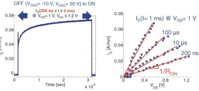
Figure 2-1. ID waveform measured by pulsed IV system. The device is synchronously switched from an OFF-state quiescent bias of VGSQ=-10 V, VDsQ=50 V to an ON-state of VGs=l V and VDs changing from 50 mV to 1.2 V at ambient temperature of 25 *C. Through the simultaneous measurement of both ID(t) and VDs(t) transients in the linear regime, the instantaneous RON(200 ns
<t < 3 ms) is extracted as shown on the right.
With the pulsed IV system, we successively switch from an OFF-state quiescent (Q) bias to an ON state given by VGs=l V and several VDS values in the linear regime of device operation (<1.2 V). In this manner, we measure the linear drain current characteristics close to the origin. Figure 2-1 shows a typical measured ID waveform in a high-voltage GaN HEMT after it is switched from an OFF-state (VGSQ= -10 V, VDSQ= 50 V) to the ON-state. ID(t) and VDS(t) are measured every 200 ns within a pulse width of 3 ms and a duty cycle of 10%. For each data point, the measurement time is 5 ns. To minimize noise and enhance measurement accuracy, each extracted data point represents an average of 300 measurements. As a result of heavy electron trapping that occurs during the OFF-state period, ON-state ID in the linear regime shows a very slow increase in time towards the expected DC value. In addition, since the pulsed IV system itself has an internal source resistance, as the device RON decreases, the range of VDS values in the ON state decreases accordingly. Through the simultaneous measurement of both ID(t) and
VDs(t) transients in the linear regime (Figure 2-1 right), the instantaneous RON(200 ns < t < 3 ms) can be extracted.
9
Pulsed IV Semiconductor Device Analyzer8-E
z 06-RON DC=
5.2 Q mm
10-7
1~7110-101
410-1072
101
1 00
101 102
103
Time
[sec]
Figure 2-2. RON transients from 200 ns up to 1,000 s on GaN-on-SiC high voltage HEMTs
from an OFF-state (VGSQ=-5 V, VDSQ=40 V) to ON-state switching at ambient temperature of 55 'C. Blue line is obtained from pulsed IV system (Auriga AU4750) and red line from semiconductor device analyzer (Agilent B1500A). Also shown is the DC values of RON obtained after fully
detrapping the device (marked as RON_Dc). This shows 66% higher RON at 200 ns than in DC.
RON transients for longer time periods can be explored using the SDA. The synchronous pulsed mode of the B 1500A allows the continuous measurement of the RON transient from 3 ms to any arbitrary
time. In contrast to the pulsed IV system, B1500A can measure ID(t) transients at a constant VDs value
(0.5 V has been used here). By adjusting the time that the device resides in the OFF state, one can closely match the beginning of the transient as measured by the SDA with the end point of the transient measurement obtained by the pulsed I-V system and obtain a complete transient that spans many decades in time. One example is shown in Figure 2-2 for transients obtained over 10 decades in time. The blue
line is measured from the pulsed IV system and the red one comes from SDA. Also shown is the DC value of RON obtained after fully detrapping the device under visible light illumination.
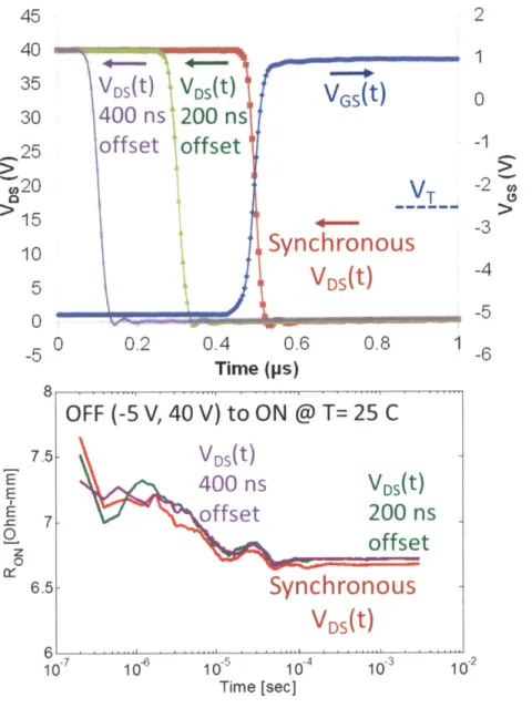
In these synchronous pulsed measurements using the pulsed I-V system and the SDA, fast switching of VGs and VDS is important so as to prevent the occurrence of a momentary high power state
during the transition ("hard" switching). Figure 2-3 shows waveforms of three different switching events from the OFF state (VGSQ= -5 V, VDSQ= 40 V) to the ON state in one of our test samples. These measurements are obtained through the pulsed I-V system. In one event, the pulsing of VDS and VGS is
synchronous. In the other two events, a delay of 200 ns or 400 ns is introduced between the switching off of VDS and the switching on of VGS. The corresponding RON transient measurements are shown below.
The time lapse between samples in the waveforms at the top of Figure 2-3 is 5 ns. With our relatively small size devices, when tested through the pulsed I-V system, a fast slew late of 1 V/ns is measured. In the synchronous case, this results in a very short overlap (a few ns) of the VDS and VGS waveforms at relatively low values of VDS. This does not introduce any visible trapping in the device as evidenced by the resulting RON transients which are essentially identical to those obtained when a delay of 200 ns or 400 ns is introduced between the two pulses. The situation might be different in the case of large size devices where the slew rate can be significantly slower and an adjustment of the delay time between VDS and VGS pulses might be needed.
In the synchronous pulse mode of the B 1500A, there is no way to control the relative delay between the gate and drain pulses. However, since the switching occurs on a much slower time scale and we always observe a good match of characteristics at the boundary with the data acquired from the pulsed I-V system, we conclude that any hard switching that might occur results in negligible trapping on the time scale in which we use this tool (t>3 ms).
1
2
45
4035
VDS(t)
30400 ns
25
offset
20
1510
5
0 -5 8 E 0 0 7.5 7 6.5 107 VDsMtVGSM
200 ns
offset
VT
Synchronous
VDSt
0
0.2
0.4
0.6
0.8
1
Time (ps)
OFF (-5 V, 40 V) to ON @ T= 25
C
400 ns
VDS
t
off set
200 n
offset
Synchronous
VDS
It)
10, -5 -4 10- 104 Time [sec]1
0
-1
-2
-3
-4-5
-6 0-2Figure 2-3. Top: VDs and VGS waveforms of three switching events from an OFF state
(VGSQ= -5 V, VDsQ= 40 V) to the ON state. In one event, the pulsing is synchronous. In the other two,
a delay of 200 ns or 400 ns is introduced between the falling edge of VDS and the rising edge of VGS.
Bottom: resulting RON transients are unaffected by the relative alignment of the VDs and VGs pulses
indicating that trapping during the transient is negligible. In our relatively small size devices, a fast slew late of 1 V/ns is obtained.
s
The stitching approach illustrated in Figure 2-2 is time consuming and inevitably leaves a small residual discrepancy between the measurements obtained through the two techniques at the 3 ms stitching point. This can cause noise in the final time constant spectra [4]. We have eliminated this problem by appropriately scaling the transient data obtained from the SDA. Figure 2-4 shows how this scaling works. We show here RON transients obtained with the pulsed IV system, as specified above, and the SDA. Both sets of transients are obtained with the device at the same OFF state bias point. Before the SDA measurements, the device is kept in the OFF-state for 50, 75, or 100 sec. All of them result in a visible mismatch with the pulsed IV data. As the OFF-state time increases, the initial value of RON at 3 ms
increases due to higher electron trapping. The evolution of the transient beyond that initial point, however, is independent of this initial value. This can be seen in the bottom of Figure 2-4 that graphs (RON(t) -RONDC)/ (RON(t=3 ms) - RON_DC) for the three cases. As seen, the transients closely overlap each other.
This suggests that the RON transients are largely independent of the initial value of RON at 3 ms and that simple scaling can be used to stitch the RON measurements obtained from the SDA to those derived from the pulsed-IV system.
From this study, we have synthesized the following approach to obtain complete RON transients. First, an RON transient is obtained using the pulsed IV system. Then, the OFF-state time in the B 1500A is controlled to produce an RON transient that closely matches the final value obtained from the pulsed I-V system. The residual mismatch is resolved through scaling of the B 1500A data set to match with the pulsed I-V data at t=3 ms. The overall transient is then analyzed using the time constant spectrum approach of [4].
OFF (-5 V, 40 V) to ON @ T= 25 C
-
Pulsed IV-
-
SDA -9 L I I I I -6 -5 -4 -3Time
102 -1[sec]
102 106 10Time [sec]
10 10
10 1 102 102Figure 2-4. Top: RON transients in OFF(VGsQ= -5 V, VDSQ= 40 V) to ON-state switching
from pulsed IV in the blue line and from SDA using different OFF-state times of 50, 75, or 100 sec.
A visible mismatch occurs with the pulsed IV data. Scaling the SDA-obtained data so as to match ARON(t)/ARON(3ms) makes all lines overlap each other as shown in dotted line. The bottom one shows identical normalized RON recovery rates suggesting that the RON transients are largely independent of the initial value of RON(3ms).