Publisher’s version / Version de l'éditeur:
Journal of Applied Physics, 104, 2, pp. 023530-023536, 2008
READ THESE TERMS AND CONDITIONS CAREFULLY BEFORE USING THIS WEBSITE. https://nrc-publications.canada.ca/eng/copyright
Vous avez des questions? Nous pouvons vous aider. Pour communiquer directement avec un auteur, consultez la première page de la revue dans laquelle son article a été publié afin de trouver ses coordonnées. Si vous n’arrivez pas à les repérer, communiquez avec nous à PublicationsArchive-ArchivesPublications@nrc-cnrc.gc.ca.
Questions? Contact the NRC Publications Archive team at
PublicationsArchive-ArchivesPublications@nrc-cnrc.gc.ca. If you wish to email the authors directly, please see the first page of the publication for their contact information.
NRC Publications Archive
Archives des publications du CNRC
This publication could be one of several versions: author’s original, accepted manuscript or the publisher’s version. / La version de cette publication peut être l’une des suivantes : la version prépublication de l’auteur, la version acceptée du manuscrit ou la version de l’éditeur.
For the publisher’s version, please access the DOI link below./ Pour consulter la version de l’éditeur, utilisez le lien DOI ci-dessous.
https://doi.org/10.1063/1.2957073
Access and use of this website and the material on it are subject to the Terms and Conditions set forth at
Thermal stability of SrFeO3/Al2O3 thin films: transmission electron
microscopy study and conductometric sensing response
Wang, Dashan; Tunney, Jim; Du, Xiaomei; Post, Michael; Gauvin, Raynald
https://publications-cnrc.canada.ca/fra/droits
L’accès à ce site Web et l’utilisation de son contenu sont assujettis aux conditions présentées dans le site LISEZ CES CONDITIONS ATTENTIVEMENT AVANT D’UTILISER CE SITE WEB.
NRC Publications Record / Notice d'Archives des publications de CNRC:
https://nrc-publications.canada.ca/eng/view/object/?id=69375db3-8b17-42fe-957d-a990a0a2ef6d https://publications-cnrc.canada.ca/fra/voir/objet/?id=69375db3-8b17-42fe-957d-a990a0a2ef6dThermal stability of SrFeO
3/ Al
2O
3thin films: Transmission electron
microscopy study and conductometric sensing response
Dashan Wang,1,a兲 James J. Tunney,1 Xiaomei Du,1 Michael L. Post,1 and Raynald Gauvin2
1
Institute for Chemical Process and Environmental Technology, National Research Council of Canada, Montreal Road, Ottawa, Ontario K1A 0R6, Canada
2
Department of Mining, Metallurgy and Materials Engineering, McGill University, Montreal, Quebec H3A 2B2, Canada
共Received 10 April 2008; accepted 16 May 2008; published online 28 July 2008兲
The SrFeO3/Al2O3 thin film system has been studied using transmission electron microscopy
共TEM兲. The thin films of SrFeO3 were grown by pulsed laser deposition onto single crystal and
sintered polycrystalline Al2O3 substrates at room temperature 共RT兲 and 700 ° C and subjected to annealing for various periods of time at 700– 1000 ° C. TEM characterization showed that the morphology of the film varied with changes of deposition temperature. Films deposited at RT featured a columnar structure and those deposited at 700 ° C showed layers with crystalline grains. The interfacial structures of the films remained unchanged below 700 ° C. Interfacial reactions were observed following annealing at 850 ° C for 5 h. The phase transformation at the interface was characterized for the film annealed at 1000 ° C for 5 h, for which the principal phases were identified as SrAl2−xFexO4and SrFe12−yAlyO19. Evaluation for thin film conductometric sensing applications
indicated that the untreated films deposited at 700 ° C onto both single crystal and sintered Al2O3
substrates exhibited a p-type gas sensor response to oxygen at 500 ° C. © 2008 American Institute
of Physics. 关DOI:10.1063/1.2957073兴
I. INTRODUCTION
Perovskites based on the nonstoichiometric family SrFeO2.5+x 共0 ⬍ x ⬍ 0.5兲, herein referred to as SrFeO3,
dis-play different crystal structures depending on the degree of oxygen stoichiometry.1–4 The end member phases for these compounds are the orthorhombic brownmillerite form at x ⬃ 0 and cubic or pseudocubic perovskite at x ⬎ 0.4. At inter-mediate oxygen stoichiometry, phases based on a distorted cubic structure exist; these are tetragonal and orthorhombic structures that possess longer range ordering of the oxygen sublattice.
Early studies have shown that the interrelationships of the structural and thermodynamic properties of the phases in the bulk powder state are a function of temperature and oxy-gen partial pressure.3Phase transformations are identified us-ing differential thermal analysis, thermogravimetric analysis, oxygen titration, and Mössbauer spectroscopy.2,3,5The study of the bulk electrical conductivity of the SrFeO3 system
showed that the material is a p-type semiconductor within a certain range of 兵T , P共O2兲其 with the conductivity of SrFeO3
increasing with increasing of P共O2兲,6 suggesting that this
physical property can be exploited for a number of techno-logical applications. As a result, perovskites and related ox-ides have attracted considerable interest. Efforts from re-searchers have been made on its extensive applications in a number of areas such as materials for catalysis7 and solid state gas sensors.7–12
SrFeO3 materials can be used as thin film gas sensors3,4,10,11 since the reversible uptake of oxygen at
el-evated temperatures 共400⬍ T ⬍ 600 ° C兲 can readily occur and this compositional change is accompanied by significant changes in electrical conductivity which can be monitored as the sensor transduction signal. However, the electrical and gas sensing properties of films of these material types are
strongly dependent on the cation and oxygen
stoichiometries11and film morphology.13–18Variations in mi-crostructure and chemical composition of the thin film could result in failure or drifting of the sensor signal response. In some ceramic-based gas sensors the SrFeO3 thin film gas
sensors typically have high sensitivity and rapid response to the changes of analyzed gas concentration at around 500 ° C. Hence, the SrFeO3thin films together with the substrate have to withstand such an elevated temperature in order to main-tain long term sensor functionality. However, SrFeO3 thin
film gas sensors may be unstable at higher operating tem-peratures. The films may react with the underlying substrate during the deposition process and subsequent thermal treatments.19–27Therefore, it is essential to have a full under-standing of the effects of deposition conditions on the thin film structures in order to ensure longer term signal repro-ducibility in sensor design.
In this study, thin films of SrFeO3have been grown onto
single crystal and sintered polycrystalline Al2O3 by pulsed
laser deposition 共PLD兲 techniques for investigation of inter-facial reactions using transmission electron microscopy 共TEM兲. The films have been prepared under different growth conditions and subjected to postdeposition thermal treat-ments. Sintered Al2O3 was chosen as one of the substrates
because it is a cost-effective alternate to single crystal alu-mina. Single crystalline Al2O3 has long been used as
sub-strate for the research on the SrFeO3thin film sensor devices. a兲aElectronic mail: dashan.wang@nrc.ca.
The study showed that sensing functionality of SrFeO3 is
strongly affected by the film morphology, such as grain size, texture structure, thickness and smoothness of the surface of the film, etc.3,4,10,11,15,17Unfortunately, there is lack of report for sintered Al2O3as the substrate for SrFeO3thin film
depo-sition. Investigation of the thermal stability of thin film sys-tems, especially the SrFeO3/Al2O3 共sintered Al2O3
sub-strate兲 system, becomes more significant than the other. Film structures were examined on the thin film systems grown at RT and 700 ° C. Characterization of interfacial reaction and phase transformation were realized on samples of the thin film system after additional annealing at 850 and 1000 ° C. Analytical TEM, including high resolution imaging, electron diffraction 共ED兲, and energy dispersive spectrometry, was utilized in the characterization steps. In parallel, an evalua-tion of the conductometric sensing funcevalua-tionality of the films was conducted on those films grown at 700 ° C.
II. EXPERIMENTAL PROCEDURE
A single phase SrFeO3 pellet was used as a target for
PLD. SrFeO3 thin films were deposited using the PLD
method with a Lambda Physik LPX305i, = 248 nm KrF excimer laser. Single crystal 共11¯02兲 alumina and sintered polycrystalline alumina were used as the substrates with a size of 1 ⫻ 1 cm2. Films were grown at RT and 700 ° C at a
laser pulse rate of 8 Hz and pulse duration of about 25 ns under a background oxygen pressure of 100 mTorr. Other experimental details can be found elsewhere.3,28 Thin film systems were annealed at 700 ° C for longer time periods and higher temperatures, i.e., 850 and 1000 ° C in air for the study of interfacial reactions. Both cross section and plan view specimens were prepared for TEM examination.29,30 Cross section specimens are particularly useful for TEM since imaging parallel to the film/substrate interface is pos-sible. The morphology of interfacial reaction products can be revealed in detail. Plan view specimens permit imaging nor-mal to the surface of the film providing a larger field of view. TEM characterization on the thin film systems was realized using a Philips CM20 equipped with an energy dispersive x-ray spectrometer 共EDS兲: INCA Energy TEM 200 and a Gatan UltraScan 1000 charge coupled device camera. The TEM was operated at 200 kV. High resolution imaging and ED techniques in combination with EDS chemical composi-tion analysis were used to investigate the interfacial structure of the film systems.
Electrical conductivity and sensor testing of the SrFeO3/Al2O3film systems was carried out using a two-wire
method4 in a controlled atmosphere environment. Electrical contacts were achieved by thermally depositing 200 nm Au pads directly onto the SrFeO3 films. Sheet resistances and
conductivities of the films were calculated from the resis-tance measurement and corrected for the geometrical con-figuration of the Au electrode pads and the thickness of the films, which was assumed to be the same for the thin film systems with the two different substrates. The sensing re-sponses of the films as a function of the gas composition were measured isothermally at 500 ° C. This was done by measuring the film electrical resistances as the O2/N2 gas
mixtures were varied from air to oxygen-poor 共6% O2兲 con-ditions in a stepwise manner, typically waiting 30 min before changing to the next composition. The gas was then changed in the reverse order from oxygen-poor condition to air in order to verify reversibility. More detailed experimental pro-cedures and conditions can be found elsewhere.4,10,31
III. RESULTS AND DISCUSSION
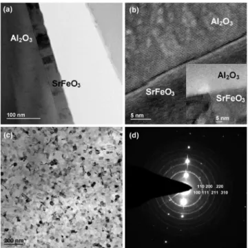
A. As-deposited SrFeO3/ Al2O3thin film system The interfacial structure of SrFeO3 deposited as a thin film onto single crystal Al2O3共sapphire兲 at 700 ° C for 4 min is shown in the TEM images of Fig.1. The average thickness of the SrFeO3 film is 38 nm and is made up of grains with boundaries that are perpendicular to the substrate. These fea-tures are shown in more detail in Fig.1共a兲. Each grain con-tains subgrains that can be identified by contrast difference in a BF image and from the lattice fringes 关Fig.1共b兲, inset兴 that indicate the associated orientation and interplanar
d-spacings. At the interface between SrFeO3 and Al2O3, as
shown in the high resolution transmission electron micros-copy 共HRTEM兲 image in Fig. 1共b兲, some atomic scaled Al2O3 lattice steps are present in a form of surface defect,
which implies that no interface interdiffusion reaction has occurred and also that the film has good adhesion to the substrate.
In the image of a plan view specimen shown in Fig.1共c兲, the SrFeO3 grain size in the layer is about 40 nm. EDS
analysis 共not shown兲 of the film indicates that the elemental composition corresponds to that of the target used in the PLD step, confirming congruent transfer during growth. The SA electron diffraction patterns 共EDPs兲 shown in Fig.1共d兲
rep-FIG. 1. 共a兲 Cross sectional TEM micrograph of the SrFeO3/Al2O3
共sap-phire兲 thin film system deposited at 700 ° C for 4 min. 共b兲 HRTEM cross sectional image showing the surface of the Al2O3substrate at the interface
and the subgrain film structure 共inset兲. 共c兲 TEM plan view micrograph of the SrFeO3film. 共d兲 SA ED pattern of the film shown in 共c兲 indicating the phase
SrFeO2.97.
resent a combination of reflections from the single crystal Al2O3substrate and the SrFeO3thin film. The ring patterns
were identified as being due to the phase SrFeO2.97共PDF file
ID No. 40–0905, cubic a0= 0.3855 nm兲 and are indexed as shown in the figure. Interpretation of the ED patterns shows no evidence of any preferential orientation of the crystalline film.
Structures of SrFeO3thin films deposited onto a sintered Al2O3substrate at RT and 700 ° C for 4 min have also been
characterized. The structure of the SrFeO3/Al2O3 共sintered兲
sample deposited at RT for 4 min is shown in the TEM micrograph of a cross section specimen 关Fig. 2共a兲兴. The thickness of the film is 56 nm. The film has a columnar structure with each column consisting of nanoscaled grains, which is also confirmed in the HRTEM image shown as the inset in Fig.2共a兲.
Columnar structures are often reported for thin film growth at low temperature. Typically, the overall morphol-ogy of the film is dramatically affected by the deposition temperature. Low temperature is in favor of nucleation of the film; however, at low temperature, limited migration or dif-fusion of the deposited species constrains the crystal growth laterally but facilitates the growth vertically during the depo-sition. As a result, a fine columnar structure is formed with a high density of crystal defects, pores, and consequent weaker adhesion to the substrate.
X-ray diffraction patterns for these films show low in-tensity and broadened peaks that could be interpreted as be-ing produced by an amorphous phase. However, the HRTEM image shown in the inset of Fig.2共a兲supports the existence of nanocrystal morphology.
Notches on the surface of the substrate in the cross sec-tion image shown in Fig.2共a兲 are due to pores that exist at the junctions of the grains of the sintered Al2O3. Although
the film lies on the substrate along the profile of the surface, gaps between film and substrate are visible as shown in Fig.
2共a兲, again indicating a poor film adhesion.
Shown in Fig. 2共b兲 is a cross section of the SrFeO3/Al
2O3 共sintered兲 thin film system grown at 700 ° C.
The thickness of the SrFeO3film is 60 nm, and it consists of a single row of grains, normal to the substrate and with simi-lar geometry to films deposited onto the single crystalline Al2O3substrate at the same temperature. Also, it is
demon-strated by ED that the crystal structure of the SrFeO3films is identical to that deposited onto single crystal Al2O3 under the same conditions. The film in the SrFeO3/Al
2O3共sintered兲
system exhibits an excellent conformation to the rough Al2O3surface, with a uniform film thickness and good adhe-sion. This is in contrast to SrFeO3 deposited onto sintered
Al2O3at room temperature, as shown in Fig. 2共a兲.
B. Postdeposition thermal treatment of the SrFeO3/ Al2O3 thin film system
1. Treatment at 700 ° C
Films of SrFeO3 deposited onto single crystal and
sin-tered Al2O3 substrates at 700 ° C for 20 min produce a
thicker film 共⬃287 nm兲 and these have been studied to ex-amine effects due to longer term thermal annealing with sub-sequent interfacial characterization. These films were an-nealed at 700 ° C for 10 h in air. The interfacial structures of the thin film system 关Fig.3共a兲兴 and the crystal structure 关see diffraction pattern shown in the inset of Fig. 3共b兲兴 and chemical composition of the film remain the same as SrFeO3,
except for having a larger grain size 关Fig. 3共b兲兴, implying that the interfaces of the thin film systems are thermally stable under these conditions.
2. Treatment at 850 ° C
Further annealing at higher temperature was conducted in order to investigate the limit of interface thermal stability of the SrFeO3/Al
2O3 thin film systems. Interfacial reactions
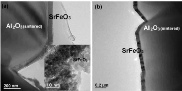
began to be observed after additional annealing at 850 ° C for 5 h 共i.e., 700 ° C for 10 h plus 850 ° C for 5 h兲. Shown in Figs.4共a兲and4共b兲are the SrFeO3thin films on single crystal
and sintered Al2O3substrates, respectively, where interfacial
reactions have occurred. At the interface, shown in Fig.4共a兲, the grains grow into the Al2O3substrate and this penetration
results in a fractal shaped boundary. Shown in the inset of Fig.4共a兲 is the fractal shaped boundary containing sections of the interface at specific orientations. These sections of interface are believed to be orientated with low interface en-ergy by forming maximum coincident lattice sites shared by both crystalline phases adjacent at the interface. The prod-ucts of the interfacial reaction are visible in the TEM image 关Fig.4共b兲兴. The grains adjacent to the film are elongated and oriented along the interface. This region is also identified by EDS as consisting of a new phase or phases due to interfacial
FIG. 2. Cross section TEM micrographs of thin film SrFeO3deposited onto
sintered Al2O3at 共a兲 RT for 4 min where column features and crystallites 共inset兲 are shown and 共b兲 deposited at 700 ° C for 4 min where monolayered grains are present.
FIG. 3. 共a兲 A cross section image and 共b兲 a plan view image, along with indexed SA diffraction patterns 共inset兲 of the SrFeO3 film deposited at
reaction. Since a quantitative analysis was not obtainable on such a limited quantity of material at the interface, conclu-sive phase identification was not determined. However, EDS analysis showed that the phases contain elemental Al and with Sr/ Fe⬍ 1 compared to SrFeO3. The ED pattern also
showed extra weak diffraction rings compared to SrFeO3.
Clearly, this is evidence that one or more new phases are forming at the interface at this stage of annealing.
3. Treatment at 1000 ° C
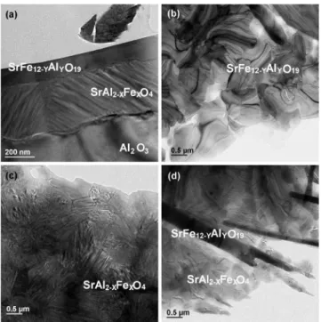
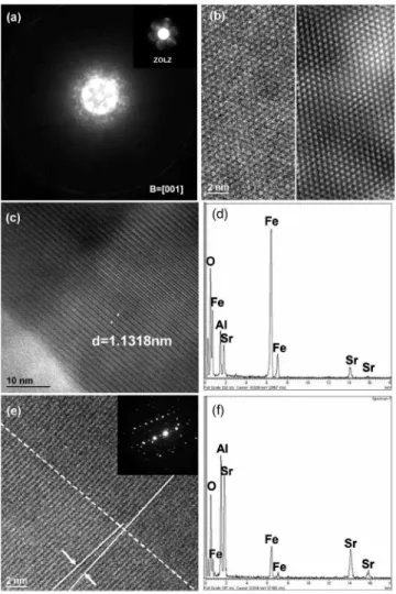
Further quantitative identification of the interfacial reac-tion features was determined on the sample annealed at 1000 ° C for 5 h, following prior annealing at 700 ° C for 10 h. Shown in Fig.5共a兲is a cross section BF TEM micrograph of this thin film system. The thin film structure consists of a
top layer and intermediate layer, each with a different mor-phology that is readily distinguished. The top layer possesses less contrast with uneven thickness ranging from 124 to 160 nm, while the intermediate layer, ranging from 290 to 400 nm in thickness, shows zones filled with bunchlike grains implying a preferential orientation. Individual layers are iso-lated and the plan view images of the top and intermediate layers are shown in Figs. 5共b兲 and 5共c兲, respectively. The grain size for the top layer 关Fig.5共b兲兴 is about the same as the zone size of the intermediate layer shown in Fig. 5共c兲. The features of the zone in the plan view image are similar to that of a zone shown in the cross section image 关Fig. 5共a兲兴, indicating that a zone is formed by stacking a number of parallel-sided slablike grains. Shown in Fig. 5共d兲 is a plan view of an area in the topmost layer. This shows a mixture of a bar-shaped phase identical to those in the top layer shown in Fig.5共b兲and the zones of the intermediate layer phase as shown in Fig.5共c兲. This implies that the intermediate phase has grown and penetrated the film to the outermost surface. Phase identification in the region of the top layer was realized by applying ED combined with EDS and HRTEM image analysis. The crystallographic information of the phase was obtained using the convergent beam electron dif-fraction 共CBED兲 technique, and the CBED pattern is shown in Fig. 6共a兲 along with the zero order Lauer zone 共ZOLZ兲 reflections 关inset of Fig. 6共a兲兴. The first order Laue zone 共FOLZ兲 reflections are present as a high intensity circle. The ZOLZ gives the two-dimensional information about the lat-tice, and the FOLZ pattern is then used to derive the third dimensional information about the lattice based on the equation32
Rⴱ⬇ 共K
t
2+ 2Hⴱ/兲1/2, 共1兲
where Kt is the component of the incident beam and Kt= 0 when the crystal is in the zone axis orientation, Rⴱ is the
radius of a high order Laue zone 共HOLZ兲 reflection ring of the reciprocal lattice, Hⴱ is the height of corresponding
HOLZ, and is the electron wavelength. Both Rⴱand Hⴱare
in reciprocal-space units 共nm−1兲.
Symmetry analysis of the CBED pattern shown in Fig.
6共a兲gives rise to the possible diffraction groups 6mm1Rand 6mm for the diffraction pattern, suggesting the type of the crystal system to be hexagonal33,34 and thus aiding lattice parameter determination. A d-spacing of d = 0.5219 nm is derived from the ZOLZ reflections, and applying Eq.共1兲the interplanar distance along the zone axis is calculated to be
H= 2.2902 nm 共H = 1 / Hⴱ兲. As a result, a hexagonal unit cell
is determined for the new phase with a = 0.6027 nm and c = 2.2902 nm.
Shown in Fig.6共b兲is a HRTEM image taken from a plan view specimen 关Fig.6共b兲, left side兴 along with a filtered im-age 关Fig.6共b兲, right side兴 produced by fast Fourier transform 共FFT兲. The image is a translation of a hexagon with side length a = 0.6034 nm, which is in agreement with the result derived from the CBED pattern. Since the zone axis of the CBED pattern is parallel to the beam and perpendicular to the thin film surface, this unique orientation relationship makes it suitable for a HRTEM cross section image of the film to acquire supplementary information about the crystal
FIG. 4. 共a兲 A cross sectional TEM image of SrFeO3/Al2O3共sapphire兲
de-posited at 700 ° C after annealing at 700 ° C for 10 h and 850 ° C for 5 h, along with a HRTEM image 共inset兲, showing a fractal interface indicated by the arrow. 共b兲 SrFeO3/Al2O3共sintered兲 film obtained following the same
conditions as 共a兲 and showing the interfacial features and new phase formation.
FIG. 5. TEM micrographs of the SrFeO3/Al2O3thin film system deposited
at 700 ° C for 20 min and annealed at 700 ° C for 10 h plus 1000 ° C for 5 h. 共a兲 Cross section image of the top and intermediate layer. 共b兲 Plan view image of the top layer. 共c兲 Plan view of the intermediate layer. 共d兲 Plan view image of an area in the top layer showing a mixture of phases from 共b兲 and 共c兲.
structure. Figure6共c兲is a HRTEM cross section image of the top layer showing a periodicity of an interplanar spacing of 1.1318 nm, which is about half of the measured H from the CBED pattern, supporting the lattice structure determined by CBED. Figure 6共d兲 is the EDS analysis on the top layer, indicating that the major elemental components in the phase are Fe and O and the minority elements are Sr with a trace of Al. The known material which can best match these data is the phase SrFe12O19 共PDF No. 33–1340, hexagonal, a
= 0.5886 nm and c = 2.3037 nm兲 with the differences in lat-tice parameters between the measured and the proposed phase being 2.3% for a and 0.5% for c. This mismatch in parameters may be due to variation in the relative elemental content, which, due to Al being present, is not precisely in the ratio of Sr:Fe:O as 1:12:19. Thus, the compositional for-mula of the phase is proposed as SrFe12−yAlyO19.
Phase identification for the intermediate layer was real-ized by microdiffraction on each grain zone. This approach was taken because each zone consists of a number of parallel-sided slablike grains acting as a single crystal with
twin boundaries or small-angle grain boundaries as the main crystal defects 关Fig.6共e兲兴; therefore, a selected area does not contain enough grains to produce an EDP with continuous rings like those shown in Fig. 1共d兲. A representative EDP from a slablike grain zone is shown in the inset of Fig.6共e兲. It is apparent that diffraction streaks have resulted from an array of slabs that are lying inversely to the thickness of the slabs and having a small orientation difference. A series of
d-spacings was obtained by taking EDPs from many grain zones, with which the d-spacings of the phase known as SrAl2O4 共PDF No. 34–0379, monoclinic, a = 0.8442 nm, b
= 0.8822 nm, and c = 0.5161 nm兲 were compared. Thus, the Bravais lattice of the phase is determined to be of the SrAl2O4type. However, information from the EDS analysis,
shown in Fig. 6共f兲, indicates that the phase also contains some Fe; therefore the formula of the phase is suggested as SrAl2−xFexO4. The Fe is assumed to substitute for Al from a
consideration of matched valency in the compound and the closer ionic radius of Fe3+共0.645 Å兲 to Al3+共0.535 Å兲 than
to Sr2+ 共1.12 Å兲.35
The growth front at the evolving interface can be found as shown in Fig. 7共a兲, which is a HRTEM image of the region between Al2O3 and SrAl2−xFexO4. The
Al2O3/SrAl2−xFexO4interface is outlined with a fractal line.
The phase SrAl2−xFexO4 penetrates the Al2O3, suggesting a
crystal structure that is evolving from SrAl2−xFexO4 into
Al2O3 and with specific orientations between the adjacent
phases. Shown in Fig.7共b兲is a HRTEM image of the region between SrAl2−xFexO4and SrFe12−yAlyO19. Unlike the fractal
feature of the Al2O3/SrAl2−xFexO4 interface, the
SrAl2−xFexO4/SrFe12−yAlyO19 interface consists of parallel
sections connected by steps of atom planes, which implies a different growth mechanism of SrAl2−xFexO4at this interface
from that at the Al2O3/SrAl2−xFexO4 interface. The phase
SrFe12−yAlyO19 is considered to be consumed during the
growth of SrAl2−xFexO4.
The orientational relationship between the crystalline SrAl2−xFexO4 growth and the Al2O3 substrate is determined
by identifying the crystal planes represented by the lattice fringes. The angle between the 共220兲 of SrAl2−xFexO4 and
共012兲 of Al2O3 is ⬃45° as shown in Fig.7共a兲. In the region
of SrAl2−xFexO4, the parallel-sided slabs are separated by
small angled boundaries as shown in Fig. 6共e兲. The angle
FIG. 6. 共a兲 CBED patterns from the top layer shown in Fig.5共b兲with ZOLZ inset. 共b兲 HRTEM image 共left兲 of the top layer and the FFT filtered image 共right兲. 共c兲 HRTEM cross section image of the top layer, the periodicity of the lattice structure is indicated. 共d兲 EDS spectra from the top layer; Al is present. 共e兲 HRTEM plan view image of the intermediate layer along with a representative EDP, indicating an interfacial relationship in a grain zone and a SrAl2O4-type crystal structure. 共f兲 EDS spectra of the intermediate layer;
Fe is present.
FIG. 7. 共a兲 HRTEM image at the SrAl2−xFexO4/Al2O3interface indicating
an irregular geometric interface and crystal orientation relationship. Twin boundaries are arrowed. 共b兲 HRTEM image at the SrFe12−yAlyO19/SrAl2−xFexO4interface.
between the planes 共220兲 of SrAl2−xFexO4 and 共001兲 of
SrFe12−yAlyO19is also about 45° as shown in Fig.7共b兲. This
match in lattice geometric orientation is presumably gov-erned by the system minimizing the interface energy. C. Chemistry of the SrFeO3/ Al2O3thin film system at 1000 ° C
The chemical reactions driving the phase transformation, as a result of the formation of the new phases, is proposed using the following sequence of equations:
6Sr2Fe2O5= 11SrO + SrFe12O19. 共2兲
Note that Sr2Fe2O5 共2SrFeO2.5兲 is used rather than SrFeO3
共SrFeO2.5+x兲 in Eq. 共2兲. This is because the oxygen
stoichi-ometry of SrFeO3 changes with the environmental
tempera-ture. At higher temperatures, ordered oxygen atoms in the octahedral positions in the SrFeO3 lattice are labile and are removed from the lattice as gas phase O2 to leave the SrFeO2.5phase.4
Equation 共2兲 describes the fact that at the interface of Al2O3/SrFeO
3, decomposition of Sr2Fe2O5 induced by
dif-fusion of Sr from Sr2Fe2O5 results in the formation of the new phase SrFe12O19. Accompanying this process, further diffusion of Sr into Al2O3 proceeds, as shown in Eq.共3兲,
Al2O3+ SrO = SrAl2O4. 共3兲
Thus, the additional phase forms, and a new interface struc-ture is created, i.e., Al2O3/SrAl2O4/SrFe12O19/SrFeO3. For
simplicity, diffusions of Fe and Al across the interfaces are not specifically shown in the equations; therefore, SrAl2O4 and SrFe12O19 represent the phases SrAl2−xFexO4 and
SrFe12−yAlyO19, respectively, and the overall reaction共4兲 is
given by combining Eqs.共2兲 and共3兲,
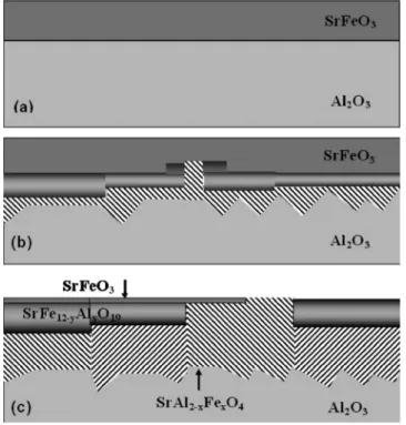
11Al2O3+ 6Sr2Fe2O5= 11SrAl2O4+ SrFe12O19. 共4兲 To further define the diffusion aspects of the interfacial reac-tions, a schematic illustration of the evolving interfacial structure of the SrFeO3/Al2O3 thin film system after
differ-ent thermal treatmdiffer-ents is shown in Fig.8. Figure8共a兲 repre-sents the structure of the SrFeO3/Al2O3 共sapphire兲 film
sys-tem deposited at 700 ° C for 20 min and annealed at 700 ° C for 10 h, where no interfacial reactions have yet initiated. Figure 8共b兲 represents the thin film system following addi-tional annealing at 850 ° C for 10 h. As a result of this ther-mal treatment, new phases now precipitate at the SrFeO3/Al
2O3interface. Shown in Fig.8共c兲is the schematic
structure of the thin film system following an additional an-neal of 10 h at 700 ° C plus a further 5 h at 1000 ° C. Figure
8共c兲now indicates the expanded depth of penetration of the new phases, SrAl2−xFexO4 and SrFe12−yAlyO19, as both the
Al2O3substrate and the initial SrFeO3 film are consumed.
D. Conductometric sensor data
SrFeO3/Al2O3 共single crystalline and sintered Al2O3兲
obtained at 700 ° C were evaluated for thin film conducto-metric sensing applications because of their good interfacial thermal stability. The results indicate that films deposited onto both single crystal and sintered Al2O3substrates
exhib-ited very similar responses to variations in oxygen concen-tration at 500 ° C 共Fig. 9兲. In both cases, changing the con-centration from 20% oxygen to 6% oxygen in balance nitrogen caused the resistance to reversibly increase approxi-mately 30%. This is indicative of the p-type semiconductor gas sensor response that it expected for SrFeO3 materials.6 This similarity of response indicates that it is legitimate to employ SrFeO3 deposited onto single crystalline Al2O3as a
model system for SrFeO3 deposited onto sintered Al2O3 commercial sensor platforms. No substantial baseline drift was observed after repeated exposures for either of these films, indicating that the interfacial diffusion is negligible at the T = 500 ° C operating temperature for this system.
FIG. 8. Schematic illustration of the interface evolution for the SrFeO3/Al2O3thin film system: 共a兲 as deposited at 700 ° C and annealed at 700 ° C for 10 h, 共b兲 after additional annealing at 850 ° C for 10 h, and 共c兲 after further annealing at 1000 ° C for 5 h.
FIG. 9. Temporal electrical resistance response of the SrFeO3 films at
500 ° C in air 共O2concentration 20%兲 when exposed to a 6% O2in /N2 mixture. Response is shown for SrFeO3on both sapphire and sintered Al2O3
substrates.
IV. CONCLUSIONS
The films of the nonstoichiometric perovskite grown onto single crystalline and sintered polycrystalline Al2O3 substrates by PLD at different temperatures with additional postdeposition thermal treatments have been characterized with TEM for the investigation of interfacial structure and reactions. The interface of the SrFeO3 films deposited onto single crystal and sintered Al2O3 substrates remained stable following thermal annealing up to 700 ° C for 10 h. Interfa-cial reactions were observed in the SrFeO3/Al2O3thin film
system after annealing at 700 ° C for 10 h followed by addi-tional annealing at 850 ° C for 5 h.
Phase transformation and reactions were characterized at the interface of the SrFeO3/Al2O3thin film system annealed
at 1000 ° C. The phases formed at the interface between SrFeO3 and Al2O3 were identified as SrAl2−xFexO4 and
SrFe12−yAlyO19.
Both systems 共SrFeO3 with single crystal and sintered
Al2O3substrates兲 show similar sensor response to oxygen at
500 ° C and can be taken as comparable sensor systems. The relative thermochemical stability of the SrFeO3/Al2O3
sys-tem below T = 700 ° C is reflected by its low baseline drift.
1J. P. Hodges, S. Short, J. D. Jorgensen, X. Xiong, B. Dabrowski, S. M.
Mini, and C. W. Kimball,J. Solid State Chem.151, 190 共2000兲.
2Y. Takeda, K. Kanno, T. Takada, O. Yamamoto, M. Takano, N. Nakayama,
and Y. Bando,J. Solid State Chem.63, 237 共1986兲.
3M. L. Post, B. W. Sanders, and P. Kennepohl,Sens. Actuators B13, 272
共1993兲.
4J. J. Tunney and M. L. Post,J. Electroceram.5, 63 共2000兲. 5S. Wimann and K. D. Becker, Solid State Ionics 85, 279 共1996兲. 6J. Hombo, Y. Matsumoto, and T. Kawano,J. Solid State Chem.84, 138
共1990兲.
7K. Ichimura, Y. Inoue, I. Yasumori, B. Viswanathan, and T. Arakawa, in
Properties and Applications of Perovskite-Type Oxides, edited by L. G. Tejuca and J. L. G. Fierro 共Marcel Dekker, New York, 1993兲, pp. 235, 271, 361.
8D. E. Williams, in Solid State Gas Sensors, edited by P. T. Moseley and B.
C. Tofield 共The Adam Hilger Series on Sensors, Bristol, Philadelphia, 1987兲, Chap. 5.
9G. Eranna, B. C. Joshi, D. P. Runthala, and R. P. Gupta,Crit. Rev. Solid
State Mater. Sci.29, 111 共2004兲.
10M. L. Post, J. J. Tunney, D. Yang, X. Du, and D. L. Singleton, Sens.
Actuators B59, 190 共1999兲.
11J. J. Tunney, M. L. Post, X. Du, and D. Yang,J. Electrochem. Soc.149,
H113 共2002兲.
12G. Martinelli, M. C. Carotta, M. Ferroni, Y. Sadaoka, and E. Traversa,
Sens. Actuators B55, 99 共1999兲.
13K. Sahner, R. Moos, M. Matam, J. J. Tunney, and M. L. Post, Sens.
Actuators B108, 102 共2005兲.
14N. Barsan and U. Weimar,J. Electroceram.7, 143 共2001兲.
15C. Xu, J. Tamaki, N. Miura, and N. Yamazoe,Sens. Actuators B3, 147
共1991兲.
16D. E. Williams and K. F. E. Pratt,Sens. Actuators B70, 214 共2000兲. 17Z. Wang, T. Sasaki, N. Koshizaki, J. J. Tunney, and M. L. Post,Thin Solid
Films437, 95 共2003兲.
18B. R. Sanders, J. Yao, and M. L. Post, Polycrystalline Thin Films:
Struc-ture, TexStruc-ture, Properties and Applications, edited by, K. Barmak, M. A. Parker, J. A. Floro, R. Sinclair, and D. A. Smith Materials Research So-ciety Symposium Proceedings No.343, San Francisco, U.S.A 1994兲, p.463.
19J. J. Tunney, P. Whitfield, X. Du, and M. L. Post, Thin Solid Films 426,
221 共2003兲.
20R. Moos, F. Rettig, A. Hürland, and C. Plog,Sens. Actuators B 93, 43
共2003兲.
21S. J. Litzelman, A. Rothschild, and H. L. Tuller,Sens. Actuators B108,
231 共2005兲.
22X.F. Chen, H. Lu, W.G. Zhu, and O.K. Tan,Surf. Coat. Technol.198, 266
共2005兲.
23S. H. Oh and C.-G. Park,Surf. Interface Anal.31, 796 共2001兲. 24X. B. Lu, X. Zhang, R. Huang, H. B. Lu, Z. H. Chen, W. F. Xiang, M. He,
B. L. Cheng, H. W. Zhou, X. P. Wang, C. Z. Wang, and B. Y. Nguyen,
Appl. Phys. Lett.84, 2620 共2004兲.
25X. B. Lu, Z. G. Liu, G. H. Shi, H. Q. Ling, H. W. Zhou, X. P. Wang, and
B. Y. Nguyen,Appl. Phys. A: Mater. Sci. Process.78, 921 共2004兲.
26J. Q. He, C. L. Jia, V. Vaithyanathan, D. G. Schlom, J. Schubert, A.
Gerber, H. H. Kohlstedt, and R. H. Wang,J. Appl. Phys. 97, 104921
共2005兲.
27D. Wang, J.J. Tunney, X. Du, M.L. Post, and R. Gauvin,J. Mater. Res.22,
1, 共2007兲.
28B. W. Sanders and M. L. Post, Laser Ablation in Materials Processing:
Fundamentals and Applications edited by B. Braren, J. J. Dubowski, and D. P. Norton, 共Materials Resarch Society, Pittsburgh PA 1993兲 Symposium Proceedings Vol. 285, p.427.
29P. J. Goodhew, Specimen Preparation for Transmission Electron
Micros-copy of Materials 共Oxford University Press, New York, 1984兲.
30D. G. Ivey and G. R. Piercy,J. Electron Microsc. Tech.8, 233 共1988兲. 31M. L. Post, J. J. Tunney, and J. Yao, Chemical and Biological Sensors and
Analytical Electrochemical Methods, The Electrochemical Society Pro-ceedings Series, edited by A. J. Ricco, M. A. Butler, P. Wanysek, G. Horvai, and A. F. Silva 共The Electrochemical Society, Inc., Pennington, NJ, 1977兲, p. 889.
32J. C. H. Spence and J. M. Zuo, Electron Microdiffraction 共Plenum Press,
New York, London, 1992兲, p. 158.
33M. H. Loretto, Electron Beam Analysis of Materials 共Chapman and Hall,
London, 1984兲, p. 88.
34B. F. Buxton, J. A. Eades, J. W. Steeds, and G. M. Rackham,Philos. Trans.
R. Soc. London, Ser. A281, 171 共1976兲.
35Edded by J. A. Dean, Lange’s Handbook of Chemistry, 15th ed.