HAL Id: hal-02917609
https://hal.univ-grenoble-alpes.fr/hal-02917609
Submitted on 18 Nov 2020HAL is a multi-disciplinary open access
archive for the deposit and dissemination of sci-entific research documents, whether they are pub-lished or not. The documents may come from teaching and research institutions in France or abroad, or from public or private research centers.
L’archive ouverte pluridisciplinaire HAL, est destinée au dépôt et à la diffusion de documents scientifiques de niveau recherche, publiés ou non, émanant des établissements d’enseignement et de recherche français ou étrangers, des laboratoires publics ou privés.
Analysis by HR-STEM of the Strain Generation in InP
after SiNx Deposition and ICP Etching
M. Gutiérrez, Df Reyes, D. Araujo, Jean-Pierre Landesman, E. Pargon
To cite this version:
M. Gutiérrez, Df Reyes, D. Araujo, Jean-Pierre Landesman, E. Pargon. Analysis by HR-STEM of the Strain Generation in InP after SiNx Deposition and ICP Etching. Journal of Electronic Materials, Institute of Electrical and Electronics Engineers, 2020, 49 (9), pp.5226-5231. �10.1007/s11664-020-08312-6�. �hal-02917609�
1
Analysis by HR-STEM of the strain generation in InP after SiN
xdeposition and ICP etching
M. Gutiérrez, D. F. Reyes and D. Araujo, University of Cadiz, Department of Materials Science, 11510 Cádiz, Spain.
J.P. Landesman, Univ Rennes, CNRS, IPR (Institut de Physique de Rennes) - UMR 6251, F-35000 Rennes, France E. Pargon, Université Grenoble Alpes, CNRS, LTM (Laboratoire des Technologies de la Microélectronique), F-38000 Grenoble, France
Abstract. Microelectronic processing to fabricate electronic devices on Si has been extensively studied and well characterized forseveral decades. This type of processing has been extrapolated for the fabrication of devices on other semiconducting materials such as Group III-Vs, SiGe and SiC. However, the structural damage and its functional implication are still not fully understood for sensitive materials like InP. The present work investigates the lattice strain induced by the ICP (inductively coupled plasma) dry etching process on InP stripes fabricated after masking the stripes with PECVD (plasma enhanced chemical vapor deposition) grown SiNx. HR-STEM (high resolution scanning transmission microscopy) observations allowed to deduce the strain at different location in the fabricated stripes. Local strains in the range of 10-3 are observed which should strongly modify the material carrier behaviour.
Introduction. Plasma etching is widely used today in the fabrication process of nanotechnology platforms, both in research, development and production, for the manufacturing of a large number of components and integrated circuits. It is used for most the known semiconducting materials, from Si to III-Vs and even for more “exotic” semiconductors such as diamond or Ga2O3. A good example of a family of such components are photonic devices that can be manufactured using InP. An noted disadvantage of plasma etching is the possible structural and chemical damage in the vicinity of the etched surfaces as well as the introduction of lattice stress and strain [1]. It is known that the mechanical stress in semiconductors alters the electrical and optical properties of the materials as a result of the bandgap modifications [2]. Indeed, small atomic-position variations and stress in the lattice bonds change the semiconductor carrier dynamics. It results in device parameters, such as the emission or absorption wavelength of a laser or detector, spectral output, current threshold, differential gain, polarization state of the output of a laser, waveguide and laser guide properties, being strongly modified. Therefore, methods to measure the material’s stress in semiconductors have been reported in the literature.
2
Measurements of uniaxial or biaxial strain in material by using photoluminescence (PL) spectroscopy [3,4]. Raman spectroscopy [5–7], transmission electron microscopy through dislocation characterisation [8–10], X-Ray diffraction [11,12], cathodoluminescence (CL) [1,13,14], using even polarized CL have been reported. However, these techniques employ indirect methods to determine strain and, in general, have low spatial resolution compared to the requirements of recent device technology processing. Micro- and nano-technology processing of components such as photonic waveguides on InP involve several steps, which can introduce significant crystal strain in, or close to, the active areas. In particular, dielectric stripes at the surface, obtained after PECVD of SiNx or SiOx thin films at moderate temperatures followed by lithography and etching generate mechanical stress which have been extensively described through the well-known edge force model [15]. Recently, detailed measurements have been published for the SiNx/InP system, using PL and CL [1,13]. In these studies, information on the local crystal strain around SiNx stripes is deduced from both the spectral shift of the luminescence lines and from measurement of the degree of polarization of the luminescence emission.
The present contribution brings additional data on this important technological question from high-resolution scanning transmission microscopy (HR-STEM) using procedures, which have been proposed for the analysis of strain at the nanoscale level [16–21]. Very local evaluation of the strain is carried out in a region of nanometerextension. Such strain may affect surface carrier behaviour as for example the channel of MOSFETs. The studied sample consists in silicon nitride stripes, deposited on an InP substrate where ICP etching is carried out after SiNx stripe deposition.
Experimental technique. The samples for this study are etched in bulk InP (100) wafers (n-type, S-doped, n=1.8x1018 cm-3) on which a 500 nm thick SiN
x hard mask layer is realized by PECVD. The etched features are rectangular-shaped lines, having lateral dimension L = 0.5, 1, 6, 10 and 20 µm, and aligned along the (110) direction of InP. These lines can be isolated, or grouped in series where the spacing between lines is S = 0.5, 1, 2, 3, 6 or 10 µm. After resist deposition, e-beam lithography, opening of this mask layer forming stripes (using a CF4/CH2F2/Ar plasma) and stripping of resist (using an O2 plasma), the SiNx patterns are transferred into the InP substrate. This is done with a CH4/Cl2/Ar plasma operated in an ICP reactor equipped with a hot cathode. During this step the samples are heated to a temperature of 200 °C. The etch rate under the conditions of this study is approximately 900 nm/min. After etching, the SiNx hard mask and the passivation layers formed on the InP sidewalls are removed by a dual step cleaning procedure using O2 plasma followed by 49% HF dip. Thus, the lattice strain revealed in the present contribution results from both technological steps: SiN mask deposition/removal and the effect of the ICP dry etching. Cross-sectional TEM lamellas were prepared by focus ion beam (FIB) and for the strain analysis a FEI TITAN3 Themis 60-300 microscope, in HR-STEM mode, was used.
3
The quantitative strain analysis in HR-STEM images is acquired at the [110] zone axis by using geometrical phase analysis (GPA) [16–23]. The lasts steps of the FIB procedure lamella thinning were carried out at 1kV ion beam accelerated voltage to avoid a possible generation of Ga implantation strain artefacts [24], that can occur above 5kV beam voltage.
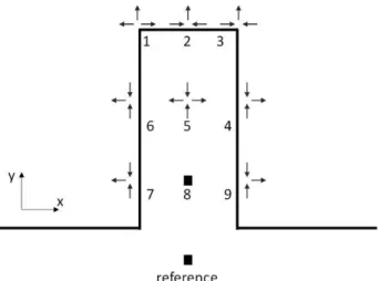
Results. Figure 1 shows the region of interest selected for this study. Four micrographs, one HAADF (high angle annular dark field) image and three EDS (electron dispersive spectroscopy) maps, are presented of a 1 µm wide stripe from the InP crystal. In- and P-mapping show the InP cross-sectional profile of the stripe. The Pt distribution corresponds to the deposition carried out in the FIB-dual beam to protect the InP stripe structure. The thickness of this Pt deposition is between 1-2µm before extracting and thinning the lamella in the lift-off FIB procedure. Once the lamella is thinned down to 100-150nm (in the present case), variations in this Pt layer are observed in the range of 0-500nm. From location to location, no strain variations are observed indicating that the Pt layer does not modify the lattice strain state of the InP. In the HAADF micrograph, we also show the locations where the high resolution STEM (HR-STEM) analysis were performed to deduce the lattice strain at different positions. The black square below the number 8 indicates the location where the reference has been taken.
Fig.1: STEM-HAADF and EDS micrographs of the studied stripe. The locations where the strain is examined are indicated in the HAADF micrograph. The EDS mapping shows the In, P and Pt chemical distributions. The latter has been deposited during the FIB-dual beam sample preparation to protect the stripe.
During the acquisition of a STEM image there are different scanning distortions. The most important source of error in the measurement of the distortion, comes from the displacement of the beam during scanning. That is, when the beam reaches the end of the ith-line, (𝑥end, 𝑦i) it should then start at the beginning of the next ith+1-line (𝑥 , 𝑦 ). This error in the return of the beam is essentially 1-D, and thus can be eliminated by choosing a
4
scanning direction parallel to the direction in which the deformation is to be studied [17–19,21], making it possible to obtain highly accurate GPA deformation maps. Therefore, in order to reduce such scanning artefacts, we followed the same experimental approach, i.e. for each studied region, two micrographs perpendicular to each other are recorded. To reduce the effects of drift, sufficient time was allowed to pass between finding a suitable position for the analysis and acquisition of the micrograph. Additionally, the acquisition time was limited to 2s, thus limiting contributions due to the drift. After minimizing the drift in the sample, we acquired pairs of micrographs, perpendicular to each other, in each area of study, aligning the scan with the direction of growth, which we have named parallel (//), and perpendicular () to the growth plane. Figure 2 shows an example of two STEM images perpendicular to each other, acquired in the area taken as reference and the deformation maps extracted from each of them, using GPA. For the choice of the reference vectors 𝑔 and 𝑔 (inset figure 2a), which will be used for the comparison of the displacements, a rectangular area has been chosen at the bottom of the image. In figure 2c and 2e artefacts due to the scanning are revealed (see arrows), which indicates that those observations must be discarded and keeping only those collinear to the scanning direction, i.e. the 𝜀 and 𝜀 for the // and , respectively. Normally, this type of analysis is carried out near interfaces or areas where there are changes in composition or crystallinity, and the reference area for choosing the vectors 𝑔 and 𝑔 , are within the image one want to analyse. However, because of the significant distance between one region and another in the present study, a different procedure should be here applied. The reference vectors 𝑔 and 𝑔 used in the GPA are carried out from the area labelled here “reference” area (see figure 1), located far from the stripe (>2µm far in the direction of the substrate), where the effects of the lithography processes are below the strain noise. This allows us to estimate the strain variations in the different study areas (numbers 1 to 9) that are far from each other. The calculation of the strain at each point in the micrographs is given by:
𝜀 , , =
, ,
, (1)
where i refers to the or // direction with respect to the plane surface, n to the region where the strain is estimated (number 1 to 9), 𝑎, to the or // lattice parameter in the region n, 𝑎, to the one of the
5
Fig.2: HRSTEM images with scanning // and to growth plane (a) and (d), respectively. The maps (b) and (f) corresponds strain maps 𝜀 and 𝜀 , while the maps (c) and (e) are those that should be discarded because the scanning direction is parallel to that of the strain determination, scanning artefacts are clearly observed (see black arrows). The inset in (c) is a scheme of cross-sectional view of FIB lamella axis election. The inset in (a) show the FFT pattern of the image and the localization of vector 𝑔 and 𝑔 for strain analysis.
In Fig.3, an example of the strain mapping, recorded on the region 6 is shown. From the atomic displacement recorded in two HAADF micrographs of the same region, acquired at 0 and 90 degrees to the direction of growth, in order to scan the areas parallel to the strain that is to be measured, xx and yy are recorded in Figs.3b and 3c respectively. Fig.3b has more regions where the average strain is positive and is measured to be 222 x 10 -5 while Fig.3c has an average strain that is negative and was found to be -164 x 10-5. Focusing the attention to the strain observed in the reference zone, one can notice the presence of a non-zero strain (Table I).. To measure these fluctuations, which will indicate the accuracy of the measurement, a small region of image has been taken where no noticeable fluctuations were observed. This sub-region was used to determine the average strain in the reference region, and the value shown in the Table I (reference) is the average strain of all image. At this point it should be noted that 𝑎, in equation one refers to 𝑎 for the sub region in the reference area.
6
The latter depends strongly on the stability of the sample below the e-beam. If no drift, no charging effects and resistance to the high energetic incident electron bombardment of the e-beam occur, then larger integration times could be used and lower noise levels can be obtained. Here, the scanning acquisition used an estimated convergence angle of 16 mrad using a camera length of 46 mm. However, these are sufficient to detect important strain variations induced by the SiNx deposition and the ICP process.
Fig.3: (a) HR-STEM micrograph in location 6, where strain evaluation has been carried out, (b) and (c) Strain distribution obtained by the atomic displacement recorded in HR-STEM micrographs scanned parallel to the strain evaluation direction.
Fig.4 shows the general tendency of the strain at different locations. The black arrows indicate if the strain is compressive () or tensile () in both x and y directions. In the lateral locations as in regions 4, 6, 7, 9, yy is compressive while xx is tensile. The results are consistent between the four locations. At the edges as in locations 1 and 3, yy is tensile while xx is compressive. This is also consistent in both locations. In the middle of the stripe (location 5), between locations 4 and 6, the vertical trend is similar to what is observed on the sides but with lower values. Lowering the location towards the “bulk” material as location 8, the strain appears lower below the accuracy of the method, i.e. as low as the reference one. Note that at the location 1, xx is the inverse to that of both location 2 and 3 (see arrow in Fig. 4). However, the values are very low (see table I) and in the expected experimental noise [-60 x 10-5, +60 x 10-5, i.e. 10-4 range) even though the accuracy of the technique is much better (10-5 range). Indeed, the location where the micrograph is recorded is not rigorously symmetric between position 1&3 as the latter is closer to the centre (position 2) of the stripe than the position 1. Such little variation can also affect the deduced strains values. It is impressive that strain value as high as several 10-3 is observed. It is worth noting that the critical thickness determined by Matthews and Blakeslee (mechanical equilibrium) where plastic strain begins is below 100nm for such strain values. Obviously, this surface elastic strain is a surface effect and its value diminishes deeper into the material probably as a result of the surface
7
bend. However, the carrier dynamic could be strongly affected by such values of strain.
Fig.4: Strain tendency inside the ICP fabricated InP stripe. Surface strain is evidenced (see table I data). TABLE I: Strain values obtained in the different locations indicated in Fig.4
Region xx/10-5 yy/10-5 1 60 32 2 -60 361 3 -22 258 4 171 -71 5 48 -66 6 222 -164 7 179 -83 8 8 3 9 157 -60 reference -5 -2
The possible origins for the local crystal deformation evidenced in this work are diverse. A first possibility is the fact that the SiNx stripe which is used as the hard mask layer for ICP etching of the InP is itself highly strained, due to the difference in the thermal expansion coefficient of SiNx compared to that of InP (the temperature at which the PECVD process is carried for this layer is typically 250 °C) and to the intrinsic stress generated by ion bombardment during PECVD. However, as mentioned, this SiNx hard mask stripe has been removed prior to the HR-STEM measurements. In addition, separate micro-PL and CL experiments with InP stripes obtained with SiNx hard mask layer grown under different built-in stress conditions (both compressive and tensile) indicate that the state of crystal deformation observed in the final InP stripe – after SiNx removal – does not change with the nature of the built-in stress in the dielectric layer used as the hard mask for etching. In other words, there does not seem to be a “history effect” related to built-in stress in the hard mask dielectric layer.
8
A second possibility that could explain the residual crystal strain observed here is related to some penetration of atoms / ions / molecules active during the ICP plasma etching process into the InP crystal. Note that the sample temperature during the ICP etching is too low for classical atomic diffusion inside the InP material. However, as previously reported indicate, for the etching of GaAs or InP, channelling or high energetic ion scattering penetration can take place [25,26]. In the present case, the dominant species in the ICP plasma, probably atomic Cl or Cl-, penetrate into the InP material. This second possibility is more likely to explain our results. As a general observation, the deeper the ICP etching is, the larger is the strain difference detected either by HRSTEM or by CL and micro-PL experiments. These observations tend to confirm that ICP-related ion implantations is responsible of the induced strain observed. The details of the mechanism leading to the spatial variation of the strain (as evidenced in the present study) still remains to be proposed and established quantitatively. This will be the topic for future work, which will include finite element simulations of local crystal deformation under the presence of inhomogeneous concentration of such foreign species in InP after etching features like stripes.
Conclusion. Subsurface local elastic strain has been evaluated by HR-STEM on ICP fabricated stripes using geometrical phase analysis (GPA) method. Consistent results are obtained all along the analysed surface. A compressive lattice strain is revealed parallel to the surface with an extensive strain perpendicular to the surface, the strain perpendicular to the surface was much greater than the strain parallel to the surface (factor 3-6). In the present case, the temperature of the sample during ICP etching is too low for classical diffusion in the InP. Therefore, the observed behaviour is tentatively explained by the implantation of ICP-related ions of the dominant species in the ICP used plasma (Cl or Cl-). Strain values in the range of some percent are deduced which highlights the importance of evaluating such effects on each lithographic approach when designing device architectures.
Acknowledgments
We thank the Ministerio de Economía y Competitividad (MINECO) of the Spanish Government for funding under Grants No. TEC2017-86347-C2-1-R (DiamMOS project) and No. ESP2017-91820-EXP (Diam-Air, EXPLORA project) from FEDER funds. We thank to EU Frame- work Programme for research ¬ Innovation – H2020 for funding under Grant No. SEP-210184415 (GreenDiamond project) of H2020-LCE-2014-1.640947 program.
References
[1] M. Fouchier, N. Rochat, E. Pargon, J.P. Landesman, Polarized cathodoluminescence for strain
measurement, Rev. Sci. Instrum. 90 (2019) 043701. doi:10.1063/1.5078506.
9 1364–1373. doi:10.1109/JSTQE.2011.2108995.
[3] J.P. Landesman, Micro-photoluminescence for the visualisation of defects, stress and
temperature profiles in high-power III-V’s devices, in: Mater. Sci. Eng. B Solid-State Mater. Adv. Technol., Elsevier, 2002: pp. 55–61. doi:10.1016/S0921-5107(01)00969-2.
[4] I.C. Bassignana, C.J. Miner, N. Puetz, Photoluminescence and double-crystal x-ray study of
InGaAs/InP: Effect of mismatch strain on band gap, J. Appl. Phys. 65 (1989) 4299–4305. doi:10.1063/1.343315.
[5] F. Ureña, S.H. Olsen, J.-P.P. Raskin, Raman measurements of uniaxial strain in silicon
nanostructures, J. Appl. Phys. 114 (2013) 144507. doi:10.1063/1.4824291.
[6] C. Neumann, S. Reichardt, P. Venezuela, M. Drögeler, L. Banszerus, M. Schmitz, K. Watanabe, T.
Taniguchi, F. Mauri, B. Beschoten, S. V. Rotkin, C. Stampfer, Raman spectroscopy as probe of nanometre-scale strain variations in graphene, Nat. Commun. 6 (2015) 1–7.
doi:10.1038/ncomms9429.
[7] S. Gennari, P.P. Lottici, F. Riccò, A Raman study of the strain in InP/GaAs heterostructures grown
by MOVPE, Superlattices Microstruct. 17 (1995) 107–110. doi:10.1006/spmi.1995.1021.
[8] D. Araújo, D. González, R. García, A. Sacedón, E. Calleja, Dislocation behavior in InGaAs step- and
alternating step-graded structures: Design rules for buffer fabrication, Appl. Phys. Lett. 67 (1995) 3632. doi:10.1063/1.115341.
[9] D. González, D. Araújo, G. Aragón, R. Garcia, Work-hardening effects in the lattice relaxation of
single layer heterostructures, Appl. Phys. Lett. 71 (1997) 2475–2477. doi:10.1063/1.120092. [10] P. Perumal, J.M. Kim, Y.T. Lee, S.S. Kim, Investigations of the characteristics of strain-free
oxidation on InAlAs epilayer lattice matched to indium phosphide, Appl. Phys. Lett. 88 (2006) 201914. doi:10.1063/1.2204654.
[11] P. van der Sluis, Determination of strain in epitaxial semiconductor structures by high-resolution X-ray diffraction, Appl. Phys. A Solids Surfaces. 58 (1994) 129–134. doi:10.1007/BF00324367. [12] A. Lankinen, T. Tuomi, M. Karilahti, Z.R. Zytkiewicz, J.Z. Domagala, P.J. McNally, Y.T. Sun, F.
Olsson, S. Lourdudoss, Crystal defects and strain of epitaxial InP layers laterally overgrown on Si, Cryst. Growth Des. 6 (2006) 1096–1100. doi:10.1021/cg0503301.
[13] J.-P. Landesman, D.T. Cassidy, M. Fouchier, C. Levallois, E. Pargon, N. Rochat, M. Mokhtari, J. Jiménez, A. Torres, Mapping of mechanical strain induced by thin and narrow dielectric stripes on InP surfaces, Opt. Lett. 43 (2018) 3505. doi:10.1364/ol.43.003505.
[14] D.H. Rich, Y. Tang, H.T. Lin, Linearly polarized and time-resolved cathodoluminescence study of strain-induced laterally ordered (InP)2/(GaP)2 quantum wires, J. Appl. Phys. 81 (1997) 6837– 6852. doi:10.1063/1.365243.
[15] S.M. Hu, Film-edge-induced stress in silicon substrates, Appl. Phys. Lett. 32 (1978) 5–7. doi:10.1063/1.89840.
[16] M.J. Hÿtch, E. Snoeck, R. Kilaas, Quantitative measurement of displacement and strain fields from HREM micrographs, Ultramicroscopy. 74 (1998) 131–146.
doi:10.1016/S0304-3991(98)00035-7.
[17] G. BÁRCENA-GONZÁLEZ, M.P. GUERRERO-LEBRERO, E. GUERRERO, D. FERNÁNDEZ-REYES, D. GONZÁLEZ, A. MAYORAL, A.D. UTRILLA, J.M. ULLOA, P.L. GALINDO, Strain mapping accuracy improvement using super-resolution techniques, J. Microsc. 262 (2016) 50–58.
doi:10.1111/jmi.12341.
10 geometric phase analysis of annular dark-field images from scanning transmission electron microscopy, IEEE Electron Device Lett. 31 (2010) 854–856. doi:10.1109/LED.2010.2049562. [19] D. Cooper, T. Denneulin, N. Bernier, A. Béché, J.L. Rouvière, Strain mapping of semiconductor
specimens with nm-scale resolution in a transmission electron microscope, Micron. 80 (2016) 145–165. doi:10.1016/j.micron.2015.09.001.
[20] T. Grieb, K. Müller, R. Fritz, M. Schowalter, N. Neugebohrn, N. Knaub, K. Volz, A. Rosenauer, Determination of the chemical composition of GaNAs using STEM HAADF imaging and STEM strain state analysis, Ultramicroscopy. 117 (2012) 15–23. doi:10.1016/j.ultramic.2012.03.014. [21] Y. Zhu, C. Ophus, J. Ciston, H. Wang, Interface lattice displacement measurement to 1 pm by
geometric phase analysis on aberration-corrected HAADF STEM images, Acta Mater. 61 (2013) 5646–5663. doi:10.1016/j.actamat.2013.06.006.
[22] D. González, V. Braza, A.D. Utrilla, A. Gonzalo, D.F. Reyes, T. Ben, A. Guzman, A. Hierro, J.M. Ulloa, Quantitative analysis of the interplay between InAs quantum dots and wetting layer during the GaAs capping process., Nanotechnology. 28 (2017) 425702. doi:10.1088/1361-6528/aa83e2.
[23] D.F. Reyes, D. González, J.M. Ulloa, D.L. Sales, L. Dominguez, A. Mayoral, A. Hierro, Impact of N on the atomic-scale Sb distribution in quaternary GaAsSbN-capped InAs quantum dots,
Nanoscale Res. Lett. 7 (2012) 653. doi:10.1186/1556-276X-7-653.
[24] R. Balboni, G. Borionetti, L. Moiraghi, G. Vaccari, M.L. Polignano, G. Pietro Carnevale, F.
Cazzaniga, I. Mica, F. Sammiceli, Improved TEM Sample Preparation by Low Energy FIB for Strain Analysis by Convergent Beam Electron Diffraction, (2009) 385–396. doi:10.1149/1.3204429. [25] R. Germann, Energy dependence and depth distribution of dry etching-induced damage in III/V
semiconductor heterostructures, J. Vac. Sci. Technol. B Microelectron. Nanom. Struct. 7 (1989) 1475. doi:10.1116/1.584515.
[26] M. Rahman, Channeling and diffusion in dry-etch damage, J. Appl. Phys. 82 (1997) 2215–2224. doi:10.1063/1.366028.