HAL Id: cea-02295172
https://hal-cea.archives-ouvertes.fr/cea-02295172
Submitted on 25 Sep 2019HAL is a multi-disciplinary open access archive for the deposit and dissemination of sci-entific research documents, whether they are pub-lished or not. The documents may come from teaching and research institutions in France or abroad, or from public or private research centers.
L’archive ouverte pluridisciplinaire HAL, est destinée au dépôt et à la diffusion de documents scientifiques de niveau recherche, publiés ou non, émanant des établissements d’enseignement et de recherche français ou étrangers, des laboratoires publics ou privés.
Fine growth control of electrografted homogeneous thin
films on patterned gold electrodes
Frédéric Lebon, R. Cornut, V. Derycke, B. Jousselme
To cite this version:
Frédéric Lebon, R. Cornut, V. Derycke, B. Jousselme. Fine growth control of electrografted homoge-neous thin films on patterned gold electrodes. Electrochimica Acta, Elsevier, 2019, 318, pp.754-761. �10.1016/j.electacta.2019.06.115�. �cea-02295172�
1
Fine Growth Control of Electrografted Homogeneous Thin Films on Patterned Gold Electrodes.
F. Lebon1, R. Cornut1, V. Derycke1, B. Jousselme1*
1LICSEN, NIMBE, CEA, CNRS, Université Paris-Saclay, CEA Saclay 91191 Gif-sur-Yvette
Cedex, France. *E-mail: bruno.jousselme@cea.fr
ABSTRACT
Electrochemical grafting of two different diazonium salts was performed on patterned gold electrodes of micrometric size. One of the molecules, a tris-bipyridine iron (II) derivative (TBPFe) enables a fine control over the final thickness of the electrografted layer thanks to its redox centers that can act as intermediate for charge transfers between the solution and the working electrode. The other one, an aromatic cycle with a long fluorinated carbon chain (DzF8), forms an insulating layer that stops the charge transfer from the working electrode to the solution and thus limits the thickness of the resulting organic layer. Grafting parameters (concentration, time, tip passivation, etc.) were investigated in details. Their precise control leads to compact and homogeneous thin films. Smooth TBPFe layers with an adjustable thickness in the 5-100 nm range are obtained, while the thickness is limited to 2-6 nm in the DzF8 case. With the achieved film quality, direct metal evaporation on top of these electrodes is possible and yields 85% of working devices. Electrical measurements for the two molecules are compared for different thicknesses.
INTRODUCTION
While Self-Assembled Monolayers (SAMs) were proposed as a potential alternative to inorganic materials for electronics,[1] important improvements are needed before industrial uses can be considered. First, even though the monolayers’ fabrication is well controlled, their integration in metal/SAM/metal type of electronic devices is still a challenge since direct metal evaporation usually leads to current leakage (except in some rare and specific cases).[2, 3] Some methods give interesting results but are not suitable for high density integration, such as on-edge molecular junctions,[4] while others can lead to high density chips but can hardly be used in an industrial process, such as lift-and-float approaches[5, 6] or nanotransfer printing techniques.[7] Electrochemical grafting (ECG) of diazonium salts leads to thin films with the deposition of multilayers of molecules. The layers are thicker than SAMs and allow potentially the use of more classic top electrodes fabrication techniques, such as metal evaporation. Moreover the electrical behavior of the thin film issue from the cumulative effect of all the molecules in the layer allows to avoid long statistical measurements. Macroscopic metal-molecules-metal junctions (with a
2 surface in the 400 µm2 range) made using electrografting have already been made.[8, 9] While our
recent contributions showed interesting results on using electrografted layers as thin gate dielectrics in transistors[10] or as the active part of memristive devices,[11] a better control over the formation of the electrografted layers is needed to optimize the performances and develop new functionalities.
ECG also brings other interesting advantages. Firstly, many different types of molecules can be electrografted, since only one specific electroactive function on the molecules is needed, such as a diazonium function.[12] All the compounds have different properties, and can be grafted on many different conductors or semi-conductors, such as copper, cobalt, iron,[13] gold,[14] silicon[15] or even on some insulators like PTFE.[16] Moreover, the strong covalently bonded organic thin films (DC-Au≈262 kJ/mol, comparable to DS-Au=254 kJ/mol typical for SAMs on
gold)[17] allow their compatibility with the techniques for fabricating microelectronic devices. ECG can also be used to graft selectively different electrodes on the same chip, by using different conditions or different molecules for example.
Most ECG studies focused on the electrochemical properties of the reaction.[12, 18] Few studies showed that the layer thickness of a diazonium grafted layer can be controlled.[19-21] While these studies show that different thickness of layers can be grafted, the control of that aspect was not detailed and the substrates that were used were bulky electrodes. None of them have studied in details the influence of the different parameters on the ECG for different molecules and on patterned electrodes of micrometer size.
Figure 1. Chemical structures of the tris-bipyridine iron(II) diazonium derivate (TBPFe) and the
4-heptadecafluorobenzene diazonium salt (DzF8).
The main objectives of this study is to demonstrate the level of control that ECG can achieve in terms of thickness adjustment and compacity for organic layers with different structures and to show that such compact thin films can be used in vertical metal-molecules-metal junctions. To achieve this, two different molecules were electrografted (figure 1): the tris-bipyridine iron(II) diazonium derivate (TBPFe), which is redox-active, and the 4-heptadecafluorobenzene diazonium
3 salt (DzF8), which forms insulating layers. The important parameters for the control of the final thickness of ECG films of these molecules are determined and studied, and the differences between ECG of the two molecules is discussed. Finally, vertical metal-molecules-metal junctions incorporating both types of electrografted layers are made, in order to prove the compacity of the layers as well as their potential for future applications in electronics.
MATERIALS AND METHODS
- Fabrication of the patterned gold electrodes: The patterned gold electrodes were made using optical and e-beam lithography. A wafer of oxidized Si(100) (150 nm SiO2) (Siltronix) was
thoroughly washed in an ultrasonic bath using successively water and Decon, acetone and ethanol. It was then cleaned in an oxygen plasma using reactive-ion etching (Plassys MG200 used at 130 V and 50 µbar of O2 for 20 s). For optical lithography of the bottom electrodes, Microposit S1805
G2 was spin-coated on a wafer (60 s at 4000 rpm) and dried at 115°C for 60 s. It was then exposed through a mask to a 405 nm UV light using an MJB3 Karl Suss Photomask Aligner. The sample was then developed during 40s in a solution of Microposit MF-319 and thoroughly rinsed with water. A final step of RIE was performed using the same conditions as previously.
The electrodes used to study the impact of the width of the electrodes on the resulting thickness of the grafted layers were made by e-beam lithography. For this, MAA EL10 was spin-coated (60 s at 4000 rpm) and dried at 100°C for 60 s. A layer of PMMA was then spin-coated (60 s at 4000 rpm) on top of it and dried at 100°C for 60 s. E-beam lithography was performed using a JEOL SEM controlled by a Raith e-beam setup. The sample was developped in a solution ethanol/methylisobutylketone (1:3 in volume) for 5 s, rinsed with ethanol and dried under nitrogen. 1 nm of chromium and 20 nm of gold were evaporated under vacuum on the lithographed samples. Lift-off was performed in acetone using mild sonication. The sample was rinsed thoroughly with acetone then ethanol, and dried with nitrogen. The top contact electrodes for the electrical measurements were fabricated by optical lithography (using LOL2000/S1805 double layer resist). The resist was exposed to UV during 15 s through a mask. The sample was developed in Microposit MF-319 for 30 s, and rinsed thoroughly with water. The next step consists in evaporation under high vacuum of 10 nm of titanium then 50 nm of gold at ±5° using a MEB 450 e-gun PLASSYS. The final sample was then put in a solution of N-methyl pyrrolidone at 50°C inside an ultrasonic bath for 3 minutes, rinsed thoroughly with acetone and ethanol, and dried with nitrogen.
- ECG of diazonium salts: The diazonium salts DzF8 and TBPFe were synthesized according to the literature.10,11 Electrografting was performed in a glove box in a setup depicted in Figure 2.
4 The solution concentration were 1 mM for DzF8 and 28 µM for TBPFe in a tetrabutylammonium hexafluorophosphate/acetonitrile (TBAPF6/ACN) electrolyte, except when the influence of the
concentration was studied. Before grafting, the sample was washed by an ultrasonic treatment, 10 min in acetone and 10 min in ethanol, followed by drying with nitrogen. A homemade Teflon electrochemical cell was filled with the solution of the diazonium salt. The sample was then plunged in the cell and electrically connected with a tungsten tip fixed on a micromanipulator (Figure 2). The counter electrode was a platinum wire and the reference electrode was an Ag wire inside a solution of AgNO3 at 10 mM in TBAPF6/ACN electrolyte. The range of the cyclic
voltammetry was -2 V to 1 V vs Ag/Ag+ at 50 mV/s for TBPFe and between -1 and 0 V at 50 mV/s for DzF8, both starting at open circuit voltage. To graft the molecules on patterned electrodes a three steps process was applied: (i) linear sweep voltammetry (LSV) at 50 mV/s from the open circuit voltage to the given potential, (ii) chronoamperometry (CA) at the given potential, (iii) LSV at 50 mV/s to 0V. After grafting, the sample was washed again using an ultrasonic bath, 10 min in acetone followed by 10 min in ethanol, then dried with nitrogen flow.
Figure 2. Scheme of the ECG setup for the functionalization of patterned gold electrodes.
- Layers’ thickness measurements: Layer thickness measurements were performed by atomic force microscopy (AFM) with a PicoLE AFM by comparison between a grafted and a non-grafted electrode.
- Electrical measurements: The electrical properties of the organic layers were measured in vacuum (10-3 mbar) in a Lakeshore TTP6 probe station using an Agilent 4156C Precision Semiconductor Parameter Analyzer with a detection limit in the sub-100 fA range.
RESULTS AND DISCUSSION
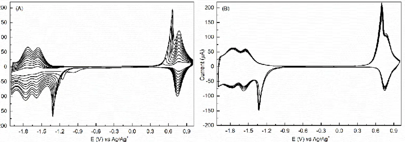
5 Cyclic voltammetry (CV) of the two (TBPFe and DzF8) molecules in TBAPF6/ACN electrolyte
on gold electrodes in a classic electrochemical cell was performed (Figure 3) to study their ECG. Concerning DzF8 (Figure 3A), during the first reduction cycle, two irreversible peaks are observed at -0.07 V and -0.57 V. These peaks are associated with the reduction of the diazonium function. When the diazonium function (N2+) is reduced, it forms a radical that reacts at the beginning with
the surface of the working electrode, and after on the already grafted layer to form a covalent bond. In litterature, the presence of two peaks was tentatively ascribed to different effects: the reduction of the diazonium function on different crystalline orientation of gold,[22] the pretreatment of the substrate[23] or two different reactions, one catalyzed and another uncatalyzed.[24] During the next cycle, the two reduction peaks can’t be seen, and the current diminishes greatly, meaning that the layer formed is more and more insulating and that the reduction process of the DzF8 is stopped. This result is coherent with the fact that DzF8 layers were observed to be insulating.[10]
Figure 3. CV at 50 mV/s of a solution of 1 mM DzF8 (A) and 28µM TBPFe (B) in 0.1M TBAPF6
in ACN on gold.
CV of TBPFe (Figure 3B) shows a very different behavior. During the first cycle, a peak around -0.30 V can barely be seen, which is attributed to the reduction of the diazonium part of TBPFe. Then, this peak vanishes and moves to lower potential for the next cycles, hidden by the other reduction peaks of the metal complexes. During the grafting, the intensity of all the peaks increases upon cycling, which shows that more and more active species are closed to the gold electrode. Multiple reversible redox couples are present: one at +0.76 V corresponding to the reversible oxidation of the iron(II) core, and two at -1.57 V and -1.77 V corresponding to the successive reversible reduction of two bipyridine ligands. Two additional peaks: one starting from -1.00 V up to -1.29 V and the other from +0.46 V up to 0.64 V can also be seen on the CV. These two peaks, still under investigation and dependent on each other as previously shown on ruthenium complexes
6 [25], can be attributed to charges trapped in the growing film or to the redox properties of the various azo bonds that are formed during the formation of the layer.
Compared to DzF8, the intensity of all the peaks increases during the electrografting of TBPFe because charges can be exchanged between the working electrode and the solution thanks to the redox properties that allow the transmission of the charges.[25] Secondly, the quantity of active species that are oxidized or reduced increases during the cycles, potential indication of the formation of a thicker layer. Finally, the CV of electrografted electrodes used as a working electrode after washing and rinsing in acetonitrile containing 0.1 M TBAPF6 shows the same peaks
than the last cycle of the CV obtained during the electrografting (Figure S1). It confirms that the redox properties of the metal complex are maintained in its electrografted form.
Thus, the two different diazonium salts with different electrochemical properties have been successfully grafted. The first one, DzF8, forms an insulating film and its grafting is self-limited. The second one, TBPFe, contains electrochemical active parts, which makes its grafting continuous. These properties have been then assessed on patterned electrodes.
2- Influence of the geometry of the electrodes on the thickness of electrografted TBPFe.
TBPFe was grafted on patterned gold electrodes made by photolithography. The electrografting
conditions used in the following part are described in the materials and methods part, with a CA time of 90 s at -1 V. The working electrode (figure 4A) is composed of different segments of different length with a width varying from 4 µm to 107 µm. AFM measurements give the final layer thickness shown in Figure 4B. The results show that the wider the electrode is, the thinner the average grafted layer. The AFM height-profile also reveals that the layer presents an edge effect : the layer is thicker near the edges of the electrode and thinner in the middle. This effect could be explained by the fact that the side of the electrode have access to a higher quantity of diazonium salts to be reduced, since the solution that is near this part and above the SiO2 substrate
can also provide diazonium salts. Both, the average thickness (evaluated in the middle of the grafted electrode by comparison with the height of the non-grafted reference electrodes) and the thickness of the edge effect increase when decreasing the width of the electrode. The relative intensity of the edge effect, shown in figure 4C, is approximately the same as the average thickness for the 107 µm width electrode and the 7 µm width. However, for the 4µm width electrode, this effect is 35% of the average thickness of the grafted layer versus a 100% increase for larger electrodes. This means that after a critical width, the average height of the grafted layer continues to increase but the intensity of the edge effect is lower when the width of the electrode diminishes. One explanation could be the following : as seen in the profile in figure 4C, the edge effects have a sharp increase near the outer part of the electrode, and then have a slow decrease in the inner part
7 of the electrode. When the electrode is thin enough, instead of being inexistent in the middle of it, the edge effects combine themselves to get a higher thickness in the middle and less “edge effect” on the outside, as shown in figure 4C.
Figure 4. (A) Optical microscope image of a TBPFE electrografted electrode (CA -1 V 45 s with
a non-passivated tip and [CTBPFE] = 23 µM) and (B) profile along the red lines corresponding to an
electrode width of 28µm (1), 7µm (2) and 4µm (3) respectively. (C) Results of the different layers’ thickness and illustration of the impact of the edge effect (black curves) on the final thickness of the grafted TBPFe layer (dotted black line) with the reduction of the width of the patterned gold electrode (yellow).
In summary, the geometry of the electrode can drastically change the homogeneity and thus the final thickness of the layer of TBPFe. Thus, in the following studies we fixed the width at 1 µm (which is more relevant than large electrodes in the perspective of developing scaled electronic devices) to determine the keys parameters involved in the control of the film thickness and solve this edge effect issue.
3- Influence of ECG parameters on the thickness of electrografted diazonium salts.
The impact of different parameters was evaluated in the following way: different electrodes of 1 µm width on the same chip were grafted separately using various conditions such as concentration of the solution, time and potential of the chronoamperometry, state of the tip (see below), etc. An example of final results after TBPFe electrografting using different potentials or different time of grafting are depicted in figure S2.
a. Influence of the diazonium concentration
The concentration of the diazonium active molecule on the final thickness of the grafted layer was first investigated. The grafting process was performed at -1 V vs Ag/Ag+ for 120s. Figure 5
displays the final thickness of TBPFe (determined by AFM) as a function of the concentration of
8 (15 and 80 µM), the final thickness barely increases. This behavior can be due to the fact that when the solution is not concentrated enough, all the species near the electrode are reduced and then mostly react with the surface for grafting or with other molecules to form polymers in solution, which creates a local drop of concentration of the species in solution in the vicinity of the electrodes. In order to continue the grafting process, molecules need to diffuse from the solution to the electrochemical double layer where the complexes get reduced and grafted. When the concentration is too low, the process is then limited by the diffusion of TBPFe in solution. When the concentration is high enough, the diffusion process is not the limiting factor, but the surface of the working electrode limits the quantity of the TBPFe molecules that can be reduced.
Figure 5. Final thickness of an electrografted layer of TBPFe versus the concentration of the
active species in a solution of 0.1 M TBAPF6 in acetonitrile using a 120s CA at -1 V vs Ag/Ag+
with a non-passivated tip. (1) Grafting limited by the local concentration of species; (2) Grafting not limited by the diffusion.
On the other hand, the final thickness of DzF8 grafted does not vary with the concentration of the diazonium salt in solution (figure S3) in the tested range (Note that at very low concentration, this parameter could play a role but thickness evolution in the sub-2nm range is both beyond our resolution and of limited relevance from a device perspective). The thickness is between 2 and 4 nm. The main difference with the TBPFe grafting is that the grafting is self-limited. Whatever the concentration of the solution, the quantity of DzF8 in solution near the working electrode is always sufficient to have the final thickness of the layer without needing the diffusion of the species after depletion of DzF8 in the double layer, hence the fact that the concentration doesn’t have any effect on the final thickness of the layer grafted.
In the following, a concentration of diazonium salts around 1mM will be used for DzF8. Since the concentration of TBPFe has a huge effect on its resulting layer, the concentration that will be used
9 for the next studies is selected on the plateau, where a small variation of concentration would not impact the resulting thickness. Thus, a concentration of 28µM of TBPFe is used in the following.
b. Influence of the ECG potential
The influence of the potential of the CA on the final thickness of the grafted layer was then studied. The influence of the potential of the ECG on the final thickness of TBPFe layers is shown Figure 6. Between -0.8 V and -1.4 V, the average thickness of the layer as well as the edge effects, represented by the maximum thickness, increase. The first increase is due to the fact that a higher potential applied gives a higher current, meaning that more species are reduced during the same time, thus giving a thicker layer. In the same way, the increase of edge effects could be due to the fact that, at a higher potential, the local concentration of species to reduce diminishes, until this concentration is close to 0 in the direct vicinity of the electrode. The next molecules to be reduced needs to diffuse from the solution to the surface of the electrode, which leads to the same behavior as the one observed above when studying the impact of concentration.
Figure 6. Final thickness of the electrografted layer of TBPFe (28 µM) (A) and DzF8 (1 mM)
(B), versus the potential applied during a 60s chronoamperometry in a solution of 0.1 M TBAPF6
in acetonitrile with a non passivated tip.
Below -1.4 V, the thickness decreases. At this potential the reduction of the ligands becomes possible and induces the formation of radical anions of metal complexes in the electrolyte. These radicals are able to decrease the resulting layer thickness as previously described.[26, 27]
The results of the grafting of DzF8 at 1 mM versus the applied potential (figure 7B) show that the lower the potential is, the thicker the layer. The final thickness of the layers are lower than those with TBPFe with a maximum thickness of 6 nm. The formed layers have no redox center and thus can’t bring the electrons from the electrode to the surface. It means that during the layer’s formation, the only electrons that can reduce new DzF8 molecules in solution are the one that can
10 pass through the formed layer by tunneling (a process that exponentially decreases with the layer thickness). Increasing the potential allows the electrons to have more energy to cross the tunneling barrier, which effectively lead to an increase of the thickness of the layer.
c. Influence of time
The influence of time on the final thickness of grafted TBPFe layer is shown in figure 7. The concentration is set at 28µM, and two grafting potentials are used : -1 V, since it seems the most promising due to the nearly nonexistent edge effects (Figure 6A), and -1.2 V, to see if the grafting can be performed faster at higher potential. The longer the CA is, the thicker the layer. Both curves has a similar slope (18.0 and 16.2 nm/min respectively), meaning that grafting at higher potential does not increase the grafting speed. In addition, it leads to a higher starting thickness (measured at the start of the CA step by extrapolating the obtained curves), which is around 5 nm for -1 V and 25 nm for -1.2 V, which is partially due to the fact that there is grafting between -1 V and -1.2 V during the LSV step. A fine control over the thickness of the TBPFe grafted layer between 5 nm and nearly 100 nm on a 1 µm width gold electrode is obtained with a grafting potential of -1 V which constitute a major achievement of this study.
Figure 7. Final thickness of an electrografted layer of TBPFe versus time of the
chronoamperometry at -1 V and -1.2 V in a solution of 0.1 M TBAPF6 and 28 µM TBPFe in
acetonitrile with a non passivated tip.
The influence of the time on the electrografting of DzF8, shown figure S4, is not surprising. All the thicknesses obtained between 10 s and 300 s of grafting are between 2.2 nm and 3.6 nm, which shows that the insulating layer is formed nearly instantly. Even with leaving the potential applied during longer time, the layer doesn’t grow further.
These studies shows how a good control over the growth of the TBPFe can be obtained. Layers as thin as 5 nm or thicker than 50 nm can be obtained in a controlled manner only by changing the
11 time of the procedure. On the other hand, DzF8 layer’s thickness can be controlled between 3 and 6 nm by changing the grafting potential, which illustrates the difference between the grafting of two different type of molecules.
d. Control over the edge effects of TBPFe
While a good control over the growth of the TBPFe layers was demonstrated in the previous parts, edge effects are still visible even at low potential, especially on samples that have a width of 8 µm. Further studies were conducted to solve this issue. First, electrografting using the best parameters determined above was performed: after the first LSV to -1 V vs Ag/Ag+, the potential used during the CA was -1 V vs Ag/Ag+ during 20 to 280 s using a tungsten tip (see figure 2 Working Electrode) in a solution of TBPFe 28 µM in acetonitrile. To passivate the surface of the tungsten tip before the electrografting of the electrode of interest, the tip was soaked in the electrolyte, connected to a unpatterned gold electrode and electrografted with TBPFe by doing 10 CV cycles between -2 V and 1 V. The aim of this step is to passivate the body of the tip while letting the part in contact with the surface of the tip non-functionalized. This passivated tungsten tip was then used to electrograft TBPFe on patterned electrodes (Figure S5). This experiment was done with a set of 24 samples, and each showed the edge effects that have been seen during the previous studies. Another tip was electrografted with the insulating DzF8 molecule by using a solution of 1 mM of
DzF8 and a gold sample using 10 CV between -1.3 V and 0 V vs Ag/Ag+. Then, the same study
as above was conducted. The optical microscope images of the sample (Figure 8A and Figure S5) show that the layer is homogeneous and no edge effects are observed. Also, the resulting layer is homogenous on areas of more than 1000 µm², such as seen in figure 8 where 130 µm of the electrode shows a homogeneous, smooth and defect-free surface at this scale.
12
Figure 8. (A) AFM image of a 150 µm part of an electrode grafted with TBPFe during a 120 s CA
with a DzF8 passivated tip at -1 V in a solution of 28 µM TBPFe and 0.1 M TBAPF6 in ACN and
(B) its corresponding profiles.
When the final layer thicknesses using a passivated tip or a non-passivated tip are compared (Figure S5), the results are similar. Thus, the tip has only an impact on the quality of the layer and its edge effect, but does not affect its average thickness. The reasons for this phenomenon are being investigated. This could be due to the fact that TBPFe passivated tip can generate radicals which would induce the edge effects, while the DzF8 passivated tip does not since its only conducting part is the part where it is connected with the gold electrode, and thus no radical species are formed near the tip. Another possible explanation involves the equilibration of electronic states of the tip and the substrate upon contact, which could lead to enhanced short time grafting with the non-passivated probe, leading to high edge effect. In any case, as the non-passivated probe removed the edge effect, we went further into the investigation to evaluate the extend of control we could achieve regarding electrografting.
Since the edge effects are solved, the impact of the size on the electrode on the final thickness of
TBPFe grafted can be reassessed. The results are shown Figure S6. Contrary to the previous
results, the final thickness of the layer grafted varies between 15 and 28 nm for a 2 min grafting and 30 to 45 nm for a 5 min grafting for a width of the electrode between 2 and 73 µm. When compared to Figure 4, the results for an electrode between 15 and 75 µm are similar for the grafting with a DzF8 passivated tip and without one, if what is compared is the average of the grafted layer. However, with an electrode of width <15 µm, the grafting with a non-passivated tip shows a sharp increase up to a layer of 120 nm thickness (Figure 4) when the width of the electrode diminishes. With a DzF8 passivated tip, the thickness stays around 20 nm for a 2 min grafting. That means that the effect of the width of the electrode is solved by passivating the tip with the DzF8, an insulating molecule. That also confirms the fact that the 120 nm layer that is obtained with the first
13 method is due to the stacking of the side effects from both sides of the electrode, increasing the average thickness of the layer grafted, as is illustrated in the scheme in the inset of Figure 4.
These studies showed that a control of the electrografting of thin layers can be achieved. The layer is smooth and without defects when using classic surface characterization tools such as AFM and optical microscopy. In order to check their real potential in electronics and confirm their compactness, their electric properties were investigated.
4- Electrical measurements of the DzF8 and TBPFe layers.
Vertical devices using TBPFe or DzF8 electrografted organic layers were fabricated using 8 µm as the width of the bottom electrodes. These electrodes are electrografted using the optimized parameters determined previously and the DzF8 passivated tip. For TBPFe, electrografting was performed during 10 s and 120 s to obtain 5 nm and 18 nm respectively (at -1 V vs Ag/Ag+ in 28 µM TBPFe in the TBAPF6/ACN electrolyte). For DzF8, electrografting was performed during
180 s at -1.3 V vs Ag/Ag+ in 0.1 mM in the TBAPF6/ACN electrolyte, which leads to a 3 nm thick
layer. Then, top electrodes composed of 10 nm of Ti and 50 nm of gold were evaporated on top through a mask made by photolithography (figure S7). The junction area was 2000 µm². Electrical measurements were performed in vacuum. The results are shown in figure 9.
Figure 9. (A) log(i) versus the potential applied for three selected junctions of 2000 µm² and (B)
statistics over the log(i) measured at 500 mV for various junctions.
The current flowing through the layer is less than 0.1 nA at 500 mV for most of the devices constituted of a layer of DzF8 3 nm thick (red) or a layer of TBPFe 18 nm thick (green). However, the devices made using a 5 nm thick layer of TBPFe (blue) typically drive current four orders of magnitude higher (average current around 1 µA at 500 mV). The difference of conductivity between a TBPFe layer and a DzF8 layer of similar thickness can be explained since
14 electrografting the DzF8 is a self-limited process and thus creates a denser layer than the grafting of TBPFe. The TBPFe layer also shows electron transport in solution, meaning that the resulting layer of TBPFe is more likely to conduct electrons in the solid state. Also, the log(i) versus V of all junctions are stable and does not show any abnormal behavior (memory or breakdown effects for example) during the measurements in this bias range, excepted for the moderate hysteresis displayed in Figure 9A.
Only few junctions show current leakage. Less than 15% of the TBPFe 18 nm junctions and DzF8 3 nm junctions have an intensity 5 decades higher than their average, which can be attributed to the current leaking through the layer, probably through a defect. However, as Figure 8 shows, even on more than 130 µm of one electrode, no defects or holes on the electrografted layer can be found at the micron scale. This means that by fabricating scaled-down devices of reduced area, the current leakage ratio is reduced.
These results show that the conducting behavior of the electrografted layer can be controlled both by changing the thickness (5 nm TBPFe versus 18 nm TBPFe) and/or changing its nature (TBPFe versus DzF8). These layers can be used on vertical metal-molecules-metal junctions of large area of contact, here 2000 µm².
CONCLUSION
In this article, we showed that electrochemical grafting of diazonium salts can be controlled to obtain different grafted layer thickness. On one hand, ECG of TBPFe, a redox active molecule, can be controlled by changing the time of the chronoamperometry and fixing the concentration of the solution and the potential of the chronoamperometry, and lead to accurately tuned thickness of grafted layers between 5 and 100 nm. On the other hand, DzF8, a molecule without redox properties except from its diazonium part, can be grafted and yields layer thickness of 3 to 6 nm by controlling the potential applied during the ECG. This technique is particularly adapated to functionalize patterned electrodes and keep the properties of the molecule used, which show great promises for future use in electronics or sensors. The optimization of the grafting was further studied by changing the experimental conditions. Thanks to that, smooth edge-less layers of
TBPFe can be grafted over very large areas. However the final thickness is highly dependent of
the geometry and the size of the patterned electrodes.
After optimizing the grafting of the two diazonium molecules, large areas of vertical metal-molecule-metal junctions have been successfully fabricated. In these devices, less than 15% of each type showed short-circuit for a surface of 2000 µm².
15 ASSOCIATED CONTENT
Supporting Information.
NOTES
The authors declare no competing financial interest.
ACKNOWLEDGMENT
This work was supported by the French National Research Agency (REMIND project – ANR-15-CE09-0001). The authors thank Olivier Segut, Laure Fillaud, Théo Cabaret, Hugo Casademont and Yu-Pu Lin for the initial developments of the setup and protocols.
REFERENCES
[1] J.C. Love, L.A. Estroff, J.K. Kriebel, R.G. Nuzzo, G.M. Whitesides, Self-Assembled Monolayers of Thiolates on Metals as a Form of Nanotechnology, Chem. Rev., 105 (2005) 1103-1170.
[2] H. Haick, O. Niitsoo, J. Ghabboun, D. Cahen, Electrical Contacts to Organic Molecular Films by Metal Evaporation:  Effect of Contacting Details, J. Phys. Chem. C, 111 (2007) 2318-2329.
[3] Y. Tai, A. Shaporenko, W. Eck, M. Grunze, M. Zharnikov, Abrupt change in the structure of self-assembled monolayers upon metal evaporation, Appl. Phys. Lett., 85 (2004) 6257-6259.
[4] W. Chen, X. Liu, Z. Tan, K.K. Likharev, J.E. Lukens, Fabrication and characterization of novel cross point structures for molecular electronic integrated circuits, J. Vac. Sci. Technol., B: Microelectron. Nanometer Struct.--Process., Meas., Phenom., 24 (2006) 3217-3220.
[5] A. Vilan, A. Shanzer, D. Cahen, Molecular control over Au/GaAs diodes, Nature, 404 (2000) 166. [6] Y. Selzer, D. Cahen, Fine Tuning of Au/SiO2/Si Diodes by Varying Interfacial Dipoles Using Molecular Monolayers, Adv. Mater., 13 (2001) 508-511.
[7] Y.-L. Loo, D.V. Lang, J.A. Rogers, J.W.P. Hsu, Electrical Contacts to Molecular Layers by Nanotransfer Printing, Nano Lett., 3 (2003) 913-917.
[8] A. Bayat, J.-C. Lacroix, R.L. McCreery, Control of Electronic Symmetry and Rectification through Energy Level Variations in Bilayer Molecular Junctions, J. Am. Chem. Soc., 138 (2016) 12287-12296.
[9] V. Rabache, J. Chaste, P. Petit, M.L. Della Rocca, P. Martin, J.-C. Lacroix, R.L. McCreery, P. Lafarge, Direct Observation of Large Quantum Interference Effect in Anthraquinone Solid-State Junctions, J. Am. Chem. Soc., 135 (2013) 10218-10221.
[10] H. Casademont, L. Fillaud, X. Lefèvre, B. Jousselme, V. Derycke, Electrografted Fluorinated Organic Ultrathin Film as Efficient Gate Dielectric in MoS2 Transistors, J. Phys. Chem. C, 120 (2016) 9506-9510. [11] Y.-P. Lin, C.H. Bennett, T. Cabaret, D. Vodenicarevic, D. Chabi, D. Querlioz, B. Jousselme, V. Derycke, J.-O. Klein, Physical Realization of a Supervised Learning System Built with Organic Memristive Synapses, Sci. Rep., 6 (2016) 31932.
[12] D. Bélanger, J. Pinson, Electrografting: a powerful method for surface modification, Chem. Soc. Rev., 40 (2011) 3995-4048.
[13] G. Lecayon, Y. Bouizem, C. Le Gressus, C. Reynaud, C. Boiziau, C. Juret, Grafting and growing mechanisms of polymerised organic films onto metallic surfaces, Chem. Phys. Lett., 91 (1982) 506-510. [14] S. Cuenot, S. Gabriel, C. Jérôme, R. Jérôme, A.-S. Duwez, Are Electrografted Polymers Chemisorbed or Physisorbed onto their Substrate?, Macromol. Chem. Phys., 206 (2005) 1216-1220.
16 [15] J. Charlier, S. Ameur, J.P. Bourgoin, C. Bureau, S. Palacin, Mask-free Localized Grafting of Organic Polymers at the Micrometer or Submicrometer Scale on Composite Conductors or Semiconductor Substrates, Adv. Funct. Mater., 14 (2004) 125-132.
[16] C. Combellas, F. Kanoufi, S. Nunige, Surface Modification of Halogenated Polymers. 10. Redox Catalysis Induction of the Polymerization of Vinylic Monomers. Application to the Localized Graft Copolymerization of Poly(tetrafluoroethylene) Surfaces by Vinylic Monomers, Chem. Mater., 19 (2007) 3830-3839.
[17] P. Doppelt, G. Hallais, J. Pinson, F. Podvorica, S. Verneyre, Surface Modification of Conducting Substrates. Existence of Azo Bonds in the Structure of Organic Layers Obtained from Diazonium Salts, Chem. Mater., 19 (2007) 4570-4575.
[18] M. Ceccato, A. Bousquet, M. Hinge, S.U. Pedersen, K. Daasbjerg, Using a Mediating Effect in the Electroreduction of Aryldiazonium Salts To Prepare Conducting Organic Films of High Thickness, Chem. Mater., 23 (2011) 1551-1557.
[19] F. Anariba, S.H. DuVall, R.L. McCreery, Mono- and Multilayer Formation by Diazonium Reduction on Carbon Surfaces Monitored with Atomic Force Microscopy "Scratching"•, Anal. Chem., 75 (2003) 3837-3844.
[20] J. Pinson, F. Podvorica, Attachment of organic layers to conductive or semiconductive surfaces by reduction of diazonium salts, Chem. Soc. Rev., 34 (2005) 429-439.
[21] P. Allongue, M. Delamar, B. Desbat, O. Fagebaume, R. Hitmi, J. Pinson, J.-M. Savéant, Covalent Modification of Carbon Surfaces by Aryl Radicals Generated from the Electrochemical Reduction of Diazonium Salts, J. Am. Chem. Soc., 119 (1997) 201-207.
[22] A. Benedetto, M. Balog, P. Viel, F. Le Derf, M. Sallé, S. Palacin, Electro-reduction of diazonium salts on gold: Why do we observe multi-peaks?, Electrochim. Acta, 53 (2008) 7117-7122.
[23] L. Lee, P.A. Brooksby, P. Hapiot, A.J. Downard, Electrografting of 4-Nitrobenzenediazonium Ion at Carbon Electrodes: Catalyzed and Uncatalyzed Reduction Processes, Langmuir, 32 (2016) 468-476. [24] K.K. Cline, L. Baxter, D. Lockwood, R. Saylor, A. Stalzer, Nonaqueous synthesis and reduction of diazonium ions (without isolation) to modify glassy carbon electrodes using mild electrografting conditions, J. Electroanal. Chem., 633 (2009) 283-290.
[25] B. Jousselme, G. Bidan, M. Billon, C. Goyer, Y. Kervella, S. Guillerez, E.A. Hamad, C. Goze-Bac, J.-Y. Mevellec, S. Lefrant, One-step electrochemical modification of carbon nanotubes by ruthenium complexes via new diazonium salts, J. Electroanal. Chem., 621 (2008) 277-285.
[26] T. Menanteau, E. Levillain, A.J. Downard, T. Breton, Evidence of monolayer formation via diazonium grafting with a radical scavenger: electrochemical, AFM and XPS monitoring, PCCP, 17 (2015) 13137-13142.
[27] L. Pichereau, I. López, M. Cesbron, S. Dabos-Seignon, C. Gautier, T. Breton, Controlled diazonium electrografting driven by overpotential reduction: a general strategy to prepare ultrathin layers, Chem. Commun., 55 (2019) 455-457.
1
Supporting Information for
Fine Growth Control of Electrografted Homogeneous Thin Films on Patterned Gold Electrodes.
F. Lebon1, R. Cornut1, V. Derycke1, B. Jousselme1
1LICSEN, NIMBE, CEA, CNRS, Université Paris-Saclay, CEA Saclay 91191 Gif-sur-Yvette
Cedex, France. E-mail: bruno.jousselme@cea.fr; Tel: +33 169089191.
Figure S1. (A) CV at 50 mV/s of a solution of 128µM TBPFe in 0.1M TBAPF6 in ACN on
2
Figure S2. (A) Optical microscope image of patterned gold electrodes electrografted with TBPFe at different potential (from -0.7 V to -1.7 V for a 120 s CA, left part) and according to
the time of the CA (from 5 s to 250 s at -1 V, right part). A DzF8 passivated tungsten tip was used. (B) AFM height profile along the red arrow of the sample electrografted with TBPFe at
3
Figure S3. Final thickness of an electrografted layer of DzF8 versus the concentration of the
active species in a solution of 0.1 M TBAPF6 in acetonitrile using a 120s CA at -1 V vs
Ag/Ag+.
Figure S4. Final thickness of an electrografted layer of DzF8 versus the time of the CA at -1 V
4
Figure S5. Optical microscope image of a sample grafted with TBPFe at -1 V for 85 s in
TBPAPF6 0.1 M in ACN with a TBPFe passivated tip (A) and its corresponding profile (B).
Optical microscope image of a sample grafted with TBPFe at -1 V for 280 s in ACN+TBAPF6
0.1 M with a DzF8 passivated tip (C) and its corresponding profile (D).
Figure S6. Final thickness of a layer of TBPFe grafted during 5 min or 2 min at -1 V versus
5
Figure S7. Optical microscope image of a typical final sample used for electrical
measurements. The orange part is the grafted bottom electrodes, the yellow parts are top electrodes.

![Figure 4. (A) Optical microscope image of a TBPFE electrografted electrode (CA -1 V 45 s with a non-passivated tip and [C TBPFE ] = 23 µM) and (B) profile along the red lines corresponding to an electrode width of 28µm (1), 7µm (2) and 4µm (3) respectiv](https://thumb-eu.123doks.com/thumbv2/123doknet/13145630.388928/8.892.111.808.227.487/optical-microscope-electrografted-electrode-passivated-corresponding-electrode-respectiv.webp)