HAL Id: hal-03024837
https://hal.archives-ouvertes.fr/hal-03024837
Submitted on 26 Nov 2020HAL is a multi-disciplinary open access
archive for the deposit and dissemination of sci-entific research documents, whether they are pub-lished or not. The documents may come from teaching and research institutions in France or abroad, or from public or private research centers.
L’archive ouverte pluridisciplinaire HAL, est destinée au dépôt et à la diffusion de documents scientifiques de niveau recherche, publiés ou non, émanant des établissements d’enseignement et de recherche français ou étrangers, des laboratoires publics ou privés.
Multi-microscopy nanoscale characterization of the
doping profile in a hybrid Mg/Ge-doped tunnel junction
E. Di Russo, A. Mavel, V Fan Arcara, B. Damilano, I Dimkou, S. Vézian, A.
Grenier, M Veillerot, N Rochat, G Feuillet, et al.
To cite this version:
E. Di Russo, A. Mavel, V Fan Arcara, B. Damilano, I Dimkou, et al.. Multi-microscopy nanoscale characterization of the doping profile in a hybrid Mg/Ge-doped tunnel junction. Nanotechnology, Institute of Physics, 2020, 31 (46), pp.465706. �10.1088/1361-6528/ab996c�. �hal-03024837�
1
Multi-microscopy nanoscale characterization of the doping profile in a hybrid
Mg/Ge-doped tunnel junction.
E. Di Russo1*, A. Mavel1, V. Fan Arcara1,2, B. Damilano2, I. Dimkou1, S. Vézian2, A. Grenier1, M. Veillerot1,N. Rochat1, G. Feuillet1, B. Bonef4, L. Rigutti5, J-Y. Duboz2, E. Monroy3, D. Cooper1
1 Univ. Grenoble Alpes, CEA, LETI, F-38000 Grenoble.
2 CNRS, Université Côte d’Azur, CRHEA, Rue Bernard Grégory, 06560 Valbonne, France. 3 Univ. Grenoble-Alpes, CEA, IRIG-PHELIQS, 17 av. des Martyrs, 38000 Grenoble, France. 4 Materials Department, University of California Santa Barbara, CA, 93106, USA.
5 UNIROUEN, INSA Rouen, CNRS, Groupe de Physique des Matériaux, Normandie Université, 76000 Rouen, France.
* Corresponding author: enrico.dirusso@cea.fr Abstract
A multi-microscopy investigation of a GaN tunnel junction (TJ) grown on an InGaN-based light emitting diode (LED) has been performed. The TJ consists of a heavily Ge-doped n-type GaN layer grown by ammonia-based molecular-beam epitaxy on a heavily Mg p-type GaN thin layer, grown by metalorganic vapor phase epitaxy. A correlation of atom probe tomography, electron holography and secondary ion mass spectrometry has been performed in order to investigate the nm-scale distribution of both Mg and Ge at the TJ. Experimental results reveal that Mg segregates at the TJ interface, and diffuses into the Ge-doped layer. As a result, the dopant concentration and distribution differ significantly from the nominal values. Despite this, electron holography reveals a TJ depletion width of ~7 nm, in agreement with band diagram simulations using the experimentally determined dopant distribution.
2 Introduction
Light emitting diodes (LEDs) based on InxGa1-xN/GaN multi-quantum wells (MQWs) are widely used as solid-state light sources [1]. The efficiency of these devices has been limited during many years by p-doping issues, due to the large activation energy of the Mg (~185 meV), the shallowest acceptor known for nitrides [2]. These problems have been solved to a satisfactory level as best blue LEDs currently have outstanding efficiencies. However, such issues remain when dealing with LEDs emitting at shorter wavelengths. For these UV LEDs, and for visible LEDs in special structures where several junctions are stacked on top of each other, tunnel junctions (TJ) have been proposed and were demonstrated to provide a good solution to the problem [3-7]. The TJ essentially consists of a degenerately doped p-n junction placed on top of the p-layer of the emitting junction, which allows effective band-to-band tunneling under reverse bias (corresponding to forward bias of the light emitting junction). The adoption of the TJ architecture mitigates the limited current spreading and reduces the contact resistance (the contact resistance of the metal/n+-GaN scheme is significantly lower than that of metal/p-GaN), without degradation of the light extraction efficiency [8-9]. Another potential advantage is the possibility to interconnect multiple active regions in cascade LEDs, in order to circumvent efficiency droop [10-11]. Finally, recent developments of growth techniques allow for the replacement of Si with Ge as the n-type dopant in GaN, achieving n-type doping levels higher than 1 × 1020 cm-3 with smoother surfaces and lower film stress than for the case of Si-doped GaN [12-15].
The challenges to implement a TJ architecture in wide bandgap materials (i.e. GaN) are strongly linked to the need to reach a sufficiently high interband tunneling probability across the depletion region. Such probability decreases exponentially with increasing TJ depletion width wd [16] which is given at zero bias by the following relation [16-18]:
𝑤 ≈ ( ) , (eq .1)
where 𝜀 is the material permittivity (9.8𝜀 for GaN, with 𝜀 the vacuum permittivity [19]), 𝑉 is the built-in potential ( 3.25 eV for GaN), 𝑁 and 𝑁 are the substitutional doping concentrations of acceptors and donors, respectively, and 𝑒 is the electron charge. As an example, with 𝑁 = 1 x 1020 cm-3 and 𝑁 = 5 x 1020 cm-3 (nominal doping of the diode studied in this article), w
d is equal to 7 nm.
In GaN-based devices, the high built-in potential (𝑉 ) and the solubility limit of the dopants make it difficult to attain high tunnel probabilities. Another specific issue arises from the passivation of Mg by hydrogen during the growth by MOCVD. Even if Mg can be activated by annealing after the p-layer growth [20-21], it is at least partially re-passivated during the subsequent growth of the n-layer on top of the p-layer to fabricate the TJ. A new approach consists of growing the n+-side of the TJ by ammonia-based molecular-beam epitaxy (NH3-MBE) directly on an LED device synthesized by metal organic chemical vapor deposition (MOCVD) [7,22].
3
This two-step growth allows post-growth annealing after the MOCVD growth. Then, during the overgrowth of n-doped GaN, the relatively low partial pressure of H2 in the NH3-MBE system prevents the re-passivation of the p-GaN layer.
The aim of the present study is to correlate the chemical, structural and electrical properties of a Mg/Ge-doped TJ grown on top of a InxGa1-xN/GaN-based LED. It has already been demonstrated that this architecture leads to an enhancement of the LED emission [22]. However, the in-depth understanding of the tunneling mechanisms requires an assessment of the distribution of dopants at the p/n interface, i.e. the MOCVD/MBE interface. A comparative multi-microscopy approach based on atomic force microscopy (AFM), off-axis electron holography, secondary ion mass spectrometry (SIMS) and laser-assisted atom probe tomography (La-APT) was adopted to obtain information about the structural properties, dopant distribution and activation. The interest of the present work is two-fold. First, it provides operational guidelines for an accurate analysis of dopant distribution at the nm scale, showing possible strengths and limitations of the different techniques. Then, the experimental results obtained represent a significant gain in the understanding of diffusion and segregation phenomena of dopants, with impact on the electrical properties of GaN-based TJs.
Materials and methods
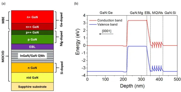
A schematic of the LED stack studied here is shown in fig. 1(a). The LED structure up to the p++-GaN layer was grown along the [0001] direction on a 2’’ sapphire substrate in an MOCVD reactor. The precursors of Ga, In, Al, Mg, Si and N were trimethylgallium (TMGa) and triethylgallium (TEGa), trimethylindium (TMIn), trimethylaluminium (TMAl), bis(cyclopentadienyl)magnesium (Cp2Mg) and ammonia (NH3), respectively. The nominal stacking sequence starts with a 1 µm non-intentionally doped (nid) GaN layer, followed by 2 µm Si-doped GaN ([Si]= 6 × 1018 cm-3). The active region consists of 5 In
xGa1-xN/GaN (6 nm / 12 nm) quantum wells. Then, a 20-nm-thick AlyGa1-yN electron blocking layer (EBL) was grown, followed by 110-nm-thick Mg-doped GaN layers (100 nm with [Mg] = 3 × 1019 cm-3 and 10 nm with [Mg] = 1 × 1020 cm-3). The LED was then annealed for 20 min at 700 °C under N2 atmosphere to activate the Mg acceptors. The wafer was transferred to an MBE Riber reactor equipped with Ga and Ge solid sources. The NH3-MBE growth of the Ge-doped GaN layers (20 nm with [Ge] = 5 × 1020 cm-3, 200 nm with [Ge] = 1 × 1019cm-3) was performed at 790 °C. The optical properties of the LED are described elsewhere [23].
4
Theoretical calculations of the band profile and electronic levels were performed using the Nextnano software [24], using the material parameters reported in ref. [25]. This software solves the Schrödinger and Poisson equations in a self-consisted manner, using the k·p model. Calculations were performed in one dimension, assuming room temperature and at zero bias. The simulated band diagram corresponding to the nominal LED structure is shown in fig. 1(b). Calculations predict an optical transition in the MQW at 431 nm, in good agreement with experimental observations (peak emission at 436 nm) [23].
Fig. 1: (a) Schematic of the blue InyGa1-yN/GaN-based LED. (b) Band diagram simulation of the structure in fig. 1(a).
To assess the sample morphology, AFM measurements were performed using a Dimension Icon AFM system operated in a tapping mode using Bruker TESPA-V2 tips.
A transmission electron microscopy (TEM) lamella specimen and needle-shaped tips required for La-APT were prepared using a FEI Helios NanoLab 450S scanning electron microscope/focused ion beam (SEM/FIB). The specimen preparation method consisted in a standard lift out procedure followed by milling with 16 kV Ga ions and cleanup procedure at 2 kV, in order to reduce the thickness of the damaged volume [26-28]. HAADF-STEM observations were carried out along the [1120] direction of the lamella specimen using an aberration corrected FEI Titan Themis operated at 200 kV. Instead, electron holography was performed along the [0120] direction using FEI Titan Ultimate operated at 200 kV. To improve the phase resolution stacks of electron holograms were recorded and then reconstructed using the Holoview software [29].
5
SIMS investigations were performed using a IMS magnetic selector instrument from CAMECA [30]. Due to the different chemical nature of Mg and Ge atoms, two measurements were carried out with optimized relative ion yields. Both Mg and Ge concentration profiles were then calculated.
Laser-assisted atom probe tomography (La-APT) was performed using a CAMECA FlexTAP system, operated at 40 K with a UV femtosecond laser (344 nm, repetition rate = 50 kHz, pulse peak energy = 2.5 × 10⁻⁴ J·cm-2). The field of view was set to 15° and detection rate to 0.0035 - 0.0050 event/pulse. Data were processed using the Tap3D software from CAMECA and homemade MATLAB codes. The 3D reconstructions were performed using a cone-angle algorithm [31].
Results and discussion
(a) Scanning Transmission Electron Microscopy
A high-angle annular dark-field scanning transmission electron microscopy (HAADF-STEM) image of the lamella specimen is shown in fig. 2(a). This imaging technique provides a signal intensity approximately proportional to the average atomic number Z². Therefore five bright layers correspond to the InxGa1-xN quantum wells, while the darker layer is the AlyGa1-yN EBL. HAADF-STEM does not reveal the chemical information from the dopants because their typical concentrations in the semiconductor samples are too low. Therefore, energy dispersion x-ray spectroscopy (EDS) was performed to obtain information about the Ge distribution. An EDS profile associated to the Ge K-line signal intensity extracted from the region indicated in fig. 2(a) along the [0001] growth direction is shown in fig. 2(b). In such a profile, the Ge signal in the n+ -layer remains below the detection threshold, but we clearly resolve the ~20-nm-thick heavily Ge-doped region, corresponding to the n++ GaN layer that is placed ~100 nm above the EBL (see fig. 1(a)). Here the Ge concentration has not been quantified due to the low signal-to-noise ratio. The EDS concentration profile of Mg cannot be detected here as the Mg K-line (1.25 keV) is very close to the Ga L-line (1.19 keV) [32].
6
Fig. 2: (a) HAADF-STEM micrograph of the lamella specimen. Only the InGaN QWs (bright contrast) and the AlGaN EBL (dark contrast) can be distinguished from the GaN background. (b) EDS intensity profile of the Ge K-line that allows locating the MOCVD/MBE interface.
(b) Atomic Force Microscopy
The HAADF-STEM cross section image shows V-shaped pits (V-pits) at the surface, with a depth that can reach ~50 nm. These irregularities of the surface can cause artifacts in chemical measurements based on top-down profiling (e.g. SIMS). Therefore, we have studied the surface morphology at a larger scale using AFM. A 2 × 2 µm2 scan of the sample surface is displayed in fig. 3(a). It confirms that V-pits appear randomly distributed with a pit density 4 × 109 cm-2. Their typical hexagonal morphology can be clearly resolved in the AFM image. The V-pits size distribution is shown in fig. 3(b). The average V-pit width is about 70 nm. It should be noted that this width measurement is reliable, but the average depth on them (~10 nm) can be strongly underestimated here due to the geometry of the AFM tip. Therefore, the cross-section TEM investigation provides a more reliable indication of the V-pit depth. The presence of these pits strongly affects the root mean square surface roughness, which was found equal to (2.5 ± 0.7) nm for the 2 × 2 µm2 AFM map. This value increases to (3.9 ± 0.7) nm for a 20 × 20 µm2 scan. As a term of comparison, AFM investigations performed before the MBE growth reveal that the p++ layer presented a very smooth surface with a roughness of ~ 0.2 nm.
7
Fig. 3: (a) AFM map of the sample surface (tapping mode). The color scale highlights the details of sample surface but does not allow measuring the interior of the V-pits. (b) Depth and width distribution of the V-pits extracted from fig. 3(a).
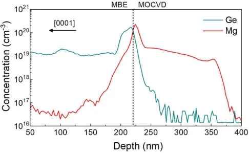
(c) Secondary Ion Mass Spectrometry
Precise quantification of the dopant concentrations was obtained by SIMS. The Mg- and Ge-doping profiles at the TJ are shown in fig. 4. The Ge concentration in the n+ GaN layer is equal to the nominal value (1 × 1019 cm-3). On the contrary, the measured Ge concentration the n++ layer reaches only 2 × 1020 cm-3, slightly lower than the targeted value. Then, in the first 30 nm of the p++ layer, the Ge concentration decreases gradually to the noise level (few 1016 cm-3). This tail is most probably an artifact originated both by the surface roughness and/or by mixing effects during SIMS measurements, as a diffusion of Ge into the p-doped region is thought to be unlikely in such a structure [33]. If we turn our attention to the distribution of Mg, the measured concentration is ~2 × 1019 cm-3 in the p layer, increases up to ~2 × 1020 cm-3 in the p++ layer. Both concentrations are slightly higher than the targeted values. Finally, a tail of Mg penetrates into the n+ GaN layer, decaying by one order of magnitude every 20 nm (i.e. the penetration of Mg into n+-GaN is too large to be an artifact). Out-diffusion of Mg can be promoted by the high substrate temperature (790 °C) during the MBE growth. Another likely explanation is Mg segregation during the MOCVD growth, and a gradual incorporation of the Mg excess in the topmost area during the MBE growth. It is important to notice that SIMS measurements do not reveal any accumulation of oxygen or carbon at the p/n interface (profiles not shown here), despite the change of growth reactor, which implied the exposure to air. All along the sample, the levels of oxygen and carbon remain below the detection limit of the setup ([O]lim = 5 × 1019 cm-3; [C]lim = 3 × 1016 cm-3).
8
It must be noted that SIMS is highly sensitive to the dopant concentration but can be limited in terms of depth resolution due to the roughening of GaN material specimen under ion irradiation. Broadening, distortions and an eventual shift of the concentration profiles are likely artifacts, which are enhanced in samples with as-grown rough surfaces. Here, the presence of V-pits inevitably affects the SIMS depth resolution, making it difficult to get accurate profiles for the Ge and Mg concentrations across the TJ interface.
Fig. 4: Mg- and Ge-doping profiles measured by SIMS. The MOCVD/MBE interface is expected to be situated between the two main concentration peaks, at a 200 nm depth.
(d) Laser-assisted Atom Probe Tomography
The spatial distribution of dopants in correspondence of the TJ has been revealed by La-APT. A 3D reconstruction of the volume around the TJ is shown in fig. 5(a) where Mg2+ ions are represented in red, while Ge2+ ions are depicted in blue. The overall volume dimension represented here is 20 × 30 × 40 nm3, corresponding to 5.3 × 10⁵ detected ions. For this 3D reconstruction, the initial tip curvature radius was set to 65 nm and the cone angle to 8°. These parameters correspond to the tip morphology measured by TEM prior to APT analysis. They allow the 3D reconstruction of the entire LED structure, showing flat interfaces and providing the nominal thicknesses of each layer.
Two distinct segments of the mass spectrum associated to the reconstructed volume are shown in fig. 5(b,c). The choice for the mass spectrum peak indexing is the same as the one commonly reported in literature [34-44]. Mg2+ cations are associated with the peaks at 12, 12.5 and 13 Da, due to its three isotopes (fig. 5(b)). However, only the principal isotope 24Mg2+ (natural abundance: 79 %) can be clearly distinguished here at 12 Da (24Mg2+ signal-to-noise ratio ≈ 4). 25Mg2+ and 26Mg2+ are partially buried inside the background noise,
9
indicating that the Mg concentration is close to the APT detection limit (~1019 cm-3) [45]. Ge2+ cations naturally occur in five isotopes forming peaks at 35, 36, 36.5, 37 and 38 Da in the mass spectrum (fig. 5(c)). However, the presence of the two thermal tails associated to Ga2+ cations appearing at 34.5 and 35.5 Da leads to an overestimation of the number of Ge atoms detected. To overcome all these limitations, a background noise correction was performed in order to calculate the number of Mg and Ge detected atoms. Despite APT providing a near-atomic scale spatial resolution, this technique still has some limitations to provide an accurate and reliable quantification of concentrations. Deviations from the stoichiometric composition were recently reported in the case of binary (i.e. GaN), ternary (i.e. AlGaN, InGaN) and heavily doped III-N semiconductors (i.e. BGaN) [34-42]. The origin of such biases is the result of the complex phenomena occurring at the tip surface during laser assisted field evaporation processes (i.e. short-range diffusion phenomena, DC-field induced preferential evaporation of metallic elements, molecular dissociation reactions, etc.). In order to mitigate such issue, the biased concentration profiles supplied by APT were corrected a posteriori using the information provided by SIMS. Briefly, it was assumed that SIMS provides an accurate quantification of the number of atoms present in each single layer of the LED stack, as indicated in fig. 4. Then, such quantities were used to normalize the APT concentration profiles, without changing the spatial distribution of atoms provided by this technique. The main limitation of this approach is that it cannot be applied for doping concentrations below the APT quantification limit (~1019 cm-3). Results are reported in fig. 5(d), where the dopant concentration profiles obtained in the TJ are represented. Data reveal a ~20 nm thick heavy Ge-doped region (~1 × 1020 cm-3), corresponding to the n++ GaN layer. The Mg concentration peak corresponding to the 10 nm thick p++ layer appears overlapped with the Ge signal at the TJ, which confirms the segregation of Mg into the n++ layer. The maximum dopant concentrations reached at the TJ are 5 × 1020 cm-3 for Mg and 2 × 10-20 cm3 for Ge. These peak values are higher than those provided by the SIMS profiles because of the smoothing induced by the low spatial resolution of SIMS (see fig. 4). In opposition to previous observation on heavy Mg-doped GaN, no Mg clustering is observed here [44].
10 (d)
Fig. 5: (a) 20 × 30 × 50 nm3 atom probe 3D reconstruction of the tunnel junction. Mg2+ ions are shown in red, Ge2+ ions appear in blue, while Ga+/++ ions are represented in green. (b,c) Detail of the atom probe mass spectrum showing the peaks associated to Mg and Ge. (d) Mg and Ge concentration profiles obtained combining the spatial distribution of dopants provided by APT with the SIMS concentration profiles.
(e) Electron Holography
APT and SIMS provide chemical information but cannot determine the electrical activity of the dopants. To be able to visualize the relative activity, off-axis electron holography was performed. Here, an electron biprism was used to create an interference pattern known as the hologram. A coherent electron wave that passes through the specimen was interfered with another that passes through vacuum. From a Fourier reconstruction procedure, information about the phase change of these electrons can be retrieved. This is
11
sensitive to the local electrostatic potential due to the presence of active dopants 𝑉 and the Mean Inner Potential (MIP) 𝑉 . The phase change ∆𝜑(𝑥, 𝑦) of an electron that passes through a specimen is given by the following equation [46]:
∆𝜑(𝑥, 𝑦) = 𝐶 ∫ 𝑉 (𝑥, 𝑦, 𝑧)𝑑𝑧, (eq. 2)
where: 𝑉 (𝑥, 𝑦, 𝑧) = 𝑉 + 𝑉 ; 𝐶 is a constant dependent on the operating voltage of the TEM, which equals to 7.3 mrad·nm-1·V-1 for 200 kV electrons; t is the thickness of the specimen. The value of the 𝑉 for GaN was calculated by density functional theory (DFT) and is found to be 16.8 V [47].
To reduce the presence of the “inactive” thickness, a relatively thick (300 nm) specimen was prepared. To avoid diffraction contrast the specimen was tilted “edge on” a few degrees from the [0120] zone axis such that the information about the different doped layers was not lost in projection. To improve the signal-to-noise ratio in the reconstructed phase images whilst reducing the effects of specimen damage and charging [44], stacks of electron holograms were acquired (32 electron holograms each acquired for 8 seconds) using a low beam current. Each electron hologram used a fringe spacing of 1.2 nm, which was reconstructed using the Holoview software to provide a nominal spatial resolution of 2.4 nm [29].
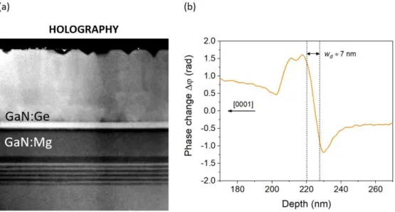
The reconstructed phase is shown in fig. 6(a). The phase image is sensitive to both the mean inner potential (MIP) and the active dopants. As the InyGa1-yN and GaN regions have very similar values of MIP [48], in the absence of diffraction contrast the phase contrast can be directly interpreted in terms of the conduction band of the stack. The AlyGa1-yN EBL appears darker as this has a lower value of MIP. In fig. 6(a) the piezoelectric fields in the five InyGa1-yN QWs can be observed; however, this experiment was not designed to resolve these structures as a thinner specimen would be required to reduce the diffraction contrast at the GaN/InyGa1-yN interfaces [49]. In the position of the TJ, a clear phase contrast change that marks the transition between the Mg- and Ge-doped GaN layers can be observed. In these experiments quantification of the phase has not been attempted as it is known that the measured potential is much less than expected for doped GaN specimens [50]. Additional attempts to quantify the potentials in p/n junction specimens has proved difficult [51]. However, in these thick specimens the measurement of the depletion width is accurate [52]. Finally, from the phase image a Δϕ profile has been extracted across the TJ and shown in fig. 6(b), where the depletion width wd can be directly measured. Assuming that the limitations from the spatial resolution provides a maximum value of the depletion width, the experimental data reveals a value of depletion width wd ≈ 7 nm, estimated from 10 % to 90 % thresholds.
12
Fig. 6: (a) Profile of the phase change ∆𝜑 across the TJ. The depletion width wd estimated from 10 % to 90 % thresholds is equal to ~7 nm. (b) Phase-contrast image from dark-field electron holography. The interface between MOCVD grown GaN and MBE grown GaN is here well resolved.
(f) Band Diagram Simulations
In order to study the effect of the dopant distribution on the electrical performance of the junction, we have calculated the band diagram of the nominal stack and compared it with the band diagram taking into account the doping profiles measured in fig. 5(d). A view of both band diagrams around the TJ is shown in fig. 7. From the simulations the width wd of the depletion region, can be measured to be ~7 nm. This result is in good agreement with the electron holography measurement (see fig. 6). The most apparent effect of Mg segregation at the MOCVD/MBE interface is to move the depletion layer by ~1 nm toward the sample surface. Note that the depletion region width in the real structure is very close to the expected width in the nominal design despite the very different distribution of dopants.
13
Fig. 7: Detail of the band diagram around the Γ-point in correspondence of the MOCVD/MBE interface. Both the nominal LED structure and a second one derived by APT observations were analyzed. The junction temperature is 300 K and no bias is applied.
Conclusions
In conclusion, we have presented a multi-microscopy study of a TJ grown on top of an InyGa1-yN /GaN LED. The TJ investigated here consists of Ge-doped layers regrown by ammonia-MBE over Mg-doped layers grown by MOCVD. A quantitative atomic-scale picture of Mg- and Ge-doping at the TJ is obtained. The high mobility of Mg atoms results in their segregation and diffusion into the n-doped GaN. The active dopant distribution revealed by electron holography shows a depletion region ~7 nm wide across the TJ. Calculations based on the experimental doping profiles provided by atom probe tomography and secondary ion mass spectrometry are in agreement with the electron holography observations. Mg diffusion phenomena result in a ~1 nm shift of the depletion region towards the n-doped GaN, although such dopant distribution appears very different compared to the nominal one. These results not only demonstrate the capabilities of the different techniques in revealing the atomic-scale dopant distribution, but also represent a significant gain in understanding the diffusion phenomena associated to the growth of hybrid Mg/Ge-doped tunnel junctions.
Acknowledgments
This work has been funded through projects DUVET (ANR project), GaNeX (GaNeX belongs to the public funded “Investissement d’Avenir” program managed by the French ANR agency and INMoSt (ANR-19-CE08-0025). The experiments have been performed on the PFNC Nanocharactersiation centre at Minatec, Grenoble.
14 Bibliography
[1] E. F. Schubert, J. K. Kim, Solid-state light sources getting smart, Science 308(5726), 1274-1278 (2005). [2] E. R. Glaser, W. E. Carlos, G. C. B. Braga, J. A. Freitas Jr., W. J. Moore, B. V. Shanabrook, R. L. Henry, A. E. Wickenden, D. D. Koleske, H. Obloh, P. Kozodoy, S. P. DenBaars, U. K. Mishra, Magnetic resonance studies of Mg-doped GaN epitaxial layers grown by organometallic chemical vapor deposition,Phys. Rev. B 65, 085312 (2002).
[3] S. R. Jeon, Y. H. Song, H. J. Jang, G. M. Yang, S. W. Hwang, S. J. Son, Lateral current spreading in GaN-based light-emitting diodes utilizing tunnel contact junctions, Appl. Phys. Lett. 78(21), 3265-3267 (2001).
[4] M. Malinverni, D. Martin, N. Grandjean, InGaN based micro light emitting diodes featuring a buried GaN tunnel junction, Appl. Phys. Lett. 107(5), 051107 (2015).
[5] A. G. Sarwar, B. J. May, J. I. Deitz, T. J. Grassman, D. W. McComb, R. C. Myers, Tunnel junction enhanced nanowire ultraviolet light emitting diodes, Appl. Phys. Lett. 107(10), 101103 (2015).
[6] Y. Zhang, S. Krishnamoorthy, F. Akyol, S. Bajaj, A. A. Allerman, M. W. Moseley, A. M. Armstrong, S. Rajan, Tunnel-injected sub-260 nm ultraviolet light emitting diodes, Appl. Phys. Lett. 110(20), 201102 (2017). [7] E. C. Young, B. P. Yonkee, F. Wu, S. H. Oh, S. P. DenBaars, S. Nakamura, J. S Speck, Hybrid tunnel junction contacts to III–nitride light-emitting diodes, Appl. Phys. Expr. 9(2), 022102 (2016).
[8] J. T. Leonard, E. C. Young, B. P. Yonkee, D. A. Cohen, T. Margalith, S. P. DenBaars, J. S Speck, S. Nakamura, Demonstration of a III-nitride vertical-cavity surface-emitting laser with a III-nitride tunnel junction intracavity contact, Appl. Phys. Lett. 107(9), 091105 (2015).
[9] H. Y. Ryu, I. G. Choi, H. S. Choi, J. I. Shim, Investigation of light extraction efficiency in AlGaN deep-ultraviolet light-emitting diodes, Appl. Phys. Expr. 6(6), 062101 (2013).
[10] F. Akyol, S. Krishnamoorthy, S. Rajan, Tunneling-based carrier regeneration in cascaded GaN light emitting diodes to overcome efficiency droop, Appl. Phys. Lett. 103(8), 081107 (2013).
[11] W. Götz, R. S. Kern, C. H. Chen, H. Liu, D. A. Steigerwald, R. M. Fletcher, Hall-effect characterization of III–V nitride semiconductors for high efficiency light emitting diodes, Mater. Sci. Eng. B 59(1-3), 211-217. (1999).
[12] S. Fritze, A. Dadgar, H. Witte, M. Bügler, A. Rohrbeck, J. Bläsing, H. Hoffmann, A. Krost, High Si and Ge n-type doping of GaN doping-Limits and impact on stress, Appl. Phys. Lett. 100(12), 122104 (2012).
[13] C. Nenstiel, M. Bügler, G. Callsen, F. Nippert, T. Kure, S. Fritze, A. Dadgar, H. Witte, J. Bläsing, A. Krost, A. Hoffmann, Germanium–the superior dopant in n-type GaN, Phys. Stat. Sol. – Rapid Research Letters 9(12), 716-721 (2015).
[14] A. Ajay, J. Schörmann, M. Jiménez-Rodriguez, C. B. Lim, F. Walther, M. Rohnke, I. Mouton, L. Amichi, C. Bougerol, M. I. Den Hertog, M. Eickhoff, E. Monroy, Ge doping of GaN beyond the Mott transition, Jour. Phys. D: Appl. Phys. 49(44), 445301 (2016).
[15] R. Blasco, A. Ajay, E. Robin, C. Bougerol, K. Lorenz, L. C. Alves, I. Mouton, L. Amichi, A. Grenier, E. Monroy, Electrical and optical properties of heavily Ge-doped AlGaN, J. Phys. D: Appl. Phys. 52, 125101 (2019). [16] H. Okumura, D. Martin, M. Malinverni, N. Grandjean, Backward diodes using heavily Mg-doped GaN growth by ammonia molecular-beam epitaxy, Appl. Phys. Lett. 108(7), 072102 (2016).
[17] S. Neugebauer, M. P. Hoffmann, H. Witte, J. Bläsing, A. Dadgar, A. Strittmatter,T. Niermann, M. Narodovitch, M. Lehmann, All metalorganic chemical vapor phase epitaxy of p/n-GaN tunnel junction for blue light emitting diode applications, Appl. Phys. Lett. 110(10), 102104 (2017).
[18] X. Yan, W. Li, S. M. Islam, K. Pourang, H. Xing, P. Fay, D. Jena, Polarization-induced Zener tunnel diodes in GaN/InGaN/GaN heterojunctions, Appl. Phys. Lett. 107(16), 163504 (2015).
15
[19] H. Morkoc, Nitride Semiconductor Devices, chap. 1, Wiley-VCH (2012).
[20] W. Li, K. Nomoto, K. Lee, S. M. Islam, Z. Hu, M. Zhu, X. Gao, J. Xie, M. Pilla, D. Jena, H. G. Xing, Activation of buried p-GaN in MOCVD-regrown vertical structures, Appl. Phys. Lett. 113(6), 062105 (2018).
[21] C. G. Van de Walle, C. Stampfl, J. Neugebauer, Theory of doping and defects in III–V nitrides, J. Cryst. Growth 189, 505-510. (1998).
[22] V. Fan Arcara, B. Damilano, G. Feuillet, S. Vézian, K. Ayadi, S. Chenot, J. Y. Duboz, Ge doped GaN and Al0.5Ga0.5N-based tunnel junctions on top of visible and UV light emitting diodes, Journ. Appl. Phys. 126(22), 224503 (2019).
[23] V. Fan Arcara, B. Damilano, G. Feuillet, S. Vézian, K. Ayadi, S. Chenot, J. Y.Duboz, Ge doped GaN and Al0. 5Ga0. 5N-based tunnel junctions on top of visible and UV light emitting diodes, Jour. Appl. Phys. 126(22), 224503 (2019).
[24] https://www.nextnano.de.
[25] T. Suski, G. Staszczak, K. P. Korona, P. Lefebvre, E. Monroy, P. A. Drozdz, G. Muzioł, C. Skierbiszewski, M. Kulczykowski, M. Matuszewski, E. Grzanka, S. Grzanka, K. Pieniak, K. Gibasiewicz, A. Khachapuridze, J. Smalc-Koziorowska, L. Marona, P. Perlin, Switching of exciton character in double InGaN/GaN quantum wells, Physical Review B, 98(16), 165302 (2018).
[26] S. Padalkar , J.R. Riley , Q. Li , G.T. Wang , L.J. Lauhon , Lift-out procedures for atom probe tomography targeting nanoscale features in core-shell nanowire heterostructures, Phys. Status Solidi C 11 (3-4), 656 (2014). [27] I. Blum , F. Cuvilly , W. Lefebvre-Ulrikson , Chapter four—Atom probe sample preparation, in: Atom Probe Tomography, Academic Press, 97–121 (2016).
[28] J. Bogdanowicz, A. Kumar, C. Fleischmann, M. Gilbert, J. Houard, A. Vella, W. Vandervorst, Laser-assisted atom probe tomography of semiconductors: The impact of the focused-ion beam specimen preparation, Ultramicroscopy 188, 19 (2018).
[29] V.Boureau, R. McLeod, B. Mayall, D. Cooper, Off-axis electron holography combining summation of hologram series with double-exposure phase-shifting: theory and application, Ultramicroscopy, 193, 52-63 (2018).
[30] www.probion.fr.
[31] D. Larson, B. Gault, B. Geiser, F. De Geuser, F. Vurpillot, Atom probe tomography spatial reconstruction: Status and directions, Current Opinion in Solid State and Materials Science 17, 236–247 (2013).
[32] S. Pezzagna, P. Vennéguès, N. Grandjean, J. Massies, Polarity inversion of GaN (0 0 0 1) by a high Mg doping, Journal of Crystal Growth 269(2-4), 249-256. (2004).
[33] Y. Oshima, Properties of Ge-doped, high-quality bulk GaN crystals fabricated by hydride vapor phase epitaxy, Journal of Crystal Growth 312, 3569-3573 (2010).
[34] E. Di Russo, I. Blum, J. Houard, M. Gilbert, G. Da Costa, D. Blavette, L. Rigutti, Compositional accuracy of atom probe tomography measurements in GaN: Impact of experimental parameters and multiple evaporation events, Ultramicroscopy 187, 126 (2018).
[35] L. Mancini, N. Amirifar, D. Shinde, I. Blum, M. Gilbert, A. Vella, F. Vurpillot, W. Lefebvre, R. Lardé, E. Talbot, P. Pareige, X. Portier, A. Ziani, C. Davesnne, C. Durand, J. Eymery, R. Butté, J.-F. Carlin, N. Grandjean, L. Rigutti, Composition of wide bandgap semiconductor materials and nanostructures measured by atom probe tomography and its dependence on the surface electric field, J. Phys. Chem. C, 118, 24136 (2014). [36] E. Di Russo, N. Cherkashin, M. Korytov, A. E. Nikolaev, A. V. Sakharov, A. F. Tsatsulnikov, B. Bonef, I. Blum, J. Houard, G. Da Costa, D. Blavette, L. Rigutti, Compositional accuracy in atom probe tomography analyses performed on III-N light emitting diodes, J. Appl. Phys. 126.12, 124307 (2019).
16
[37] E. Di Russo, F. Moyon, N. Gogneau, L. Largeau, E. Giraud, J.-F. Carlin, N. Grandjean, J. M. Chauveau, M. Hugues, I. Blum, W. Lefebvre, F. Vurpillot, D. Blavette, L. Rigutti, Composition metrology of ternary semiconductor alloys analyzed by Atom Probe Tomography, J. Phys. Chem. C 122.29, 16704-16714 (2018). [38] L. Rigutti, B. Bonef, J. Speck, F. Tang, R. A. Oliver, Atom probe tomography of nitride semiconductors, Scripta Materialia 148, 75-81 (2018).
[39] B. Bonef, R. Cramer, J. S. Speck, Nanometer scale composition study of MBE grown BGaN performed by atom probe tomography, J. Appl. Phys. 121(22), 225701 (2017).
[40] E. Di Russo, Study of the physical mechanisms leading to compositional biases in atom probe tomography of semiconductors, Ph.D thesis, Université de Rouen (2018).
[41] R. J. H. Morris, R. Cuduvally, D. Melkonyan, C. Fleischmann, M. Zhao, L. Arnoldi, P. van der Heide, and W. Vandervorst, Toward accurate composition analysis of GaN and AlGaN using atom probe tomography, J. Vac. Sci. Technol. B 36(3), 03F130 (2018).
[42] R. J. H. Morris, R. Cuduvally, D. Melkonyan, M. Zhao, P. van der Heide, W. Vandervorst, Atom probe of GaN/AlGaN heterostructures: The role of electric field, sample crystallography and laser excitation on quantification, Ultramicroscopy 206, 112813 (2019).
[43] Y. Shimizu, H. Takamizawa, Y. Kawamura, M. Uematsu, T. Toyama, K. Inoue, E. E. Haller, K. M. Itoh, Y. Nagai, Atomic-scale characterization of germanium isotopic multilayers by atom probe tomography, J. Appl. Phys. 113, 026101 (2013).
[44] L. Amichi, I. Mouton, E. Di Russo, V. Boureau, P. Vennegues, P. De Mierry, A. Grenier, P.-H. Jouneau, C. Bougerol, D. Cooper, Correlative investigation of Mg doping in GaN layers grown at different temperatures by atom probe tomography and off-axis electron holography, Nanotechnology 31(4), 045702 (2019). [45] A. M. Siladie, L. Amichi, N. Mollard, I. Mouton, B. Bonef, C. Bougerol, A. Grenier, E. Robin, P.-H. Jouneau, N. Garro, A. Cros, B. Daudin, Dopant radial inhomogeneity in Mg-doped GaN nanowires, Nanotechnology 29(25), 255706 (2018).
[46] M. McCartney, D. Smith, R. Hull, J. Bean, E. Voelkl, B. Frost, Direct observation of potential distribution across Si/Si p–n junctions using off-axis electron holography, Appl. Phys. Lett. 65(20), 2603-2605 (1994). [47] P. Kruse, M. Schowalter, D. Lamoen, A. Rosenauer, D. Gerthsen, Determination of the mean inner potential in III–V semiconductors, Si and Ge by density functional theory and electron holography, Ultramicroscopy 106, 105–13 (2006).
[48] K. Song, C. T. Koch, J. K. Lee, D. Y. Kim, , J. K. Kim, A. Parvizi, W. Y. Jung, C. G. Park, H. J. Jeong, H. S. Kim, Y. Cao, T. Yang, L.-Q. Chen, S. H. Oh, Correlative high-resolution mapping of strain and charge density in a strained piezoelectric multilayer, Advanced Materials Interfaces, 2(1), 1400281 (2015).
[49] B. Haas, J. L. Rouviere, V. Boureau, R. Berthier, D. Cooper, Direct comparison of off-axis holography and differential phase contrast for the mapping of electric fields in semiconductors by transmission electron microscopy, Ultramicroscopy, 198, 58-72 (2019).
[50] J. B. Park, T. Niermann, D. Berger, A. Knauer, I. Koslow, M. Weyers, M. Kneissl, M. Lehmann, Impact of electron irradiation on electron holographic potentiometry, Appl. Phys. Lett. 105(9), 094102 (2014).
[51] L. Amichi,Study of p-type doping in GaN nanostructures by correlation between atom probe tomography and off-axis electronic holography, Université de Grenoble (2018).
[52] P. K. Somodi, A. C. Twitchett-Harrison, P. A. Midgley, B. E. Kardynał, C. H. W. Barnes, R. E. Dunin-Borkowski, Finite element simulations of electrostatic dopant potentials in thin semiconductor specimens for electron holography. Ultramicroscopy 134, 160-166 (2013).