HAL Id: hal-02083645
https://hal.archives-ouvertes.fr/hal-02083645
Submitted on 11 Apr 2019HAL is a multi-disciplinary open access archive for the deposit and dissemination of sci-entific research documents, whether they are pub-lished or not. The documents may come from teaching and research institutions in France or abroad, or from public or private research centers.
L’archive ouverte pluridisciplinaire HAL, est destinée au dépôt et à la diffusion de documents scientifiques de niveau recherche, publiés ou non, émanant des établissements d’enseignement et de recherche français ou étrangers, des laboratoires publics ou privés.
Ballistic One-Dimensional Holes with Strong g -Factor
Anisotropy in Germanium
R. Mizokuchi, R. Maurand, F. Vigneau, M. Myronov, S. de Franceschi
To cite this version:
R. Mizokuchi, R. Maurand, F. Vigneau, M. Myronov, S. de Franceschi. Ballistic One-Dimensional Holes with Strong g -Factor Anisotropy in Germanium. Nano Letters, American Chemical Society, 2018, 18 (8), pp.4861-4865. �10.1021/acs.nanolett.8b01457�. �hal-02083645�
Ballistic one-dimensional holes with strong
g-factor anisotropy in germanium
R. Mizokuchi,
†R. Maurand,
†F. Vigneau,
†M. Myronov,
‡and S. De Franceschi
∗,††Université Grenoble Alpes & CEA, INAC-PHELIQS, F-38000 Grenoble, France ‡Department of Physics, University of Warwick, Coventry CV4 7AL, United Kingdom
E-mail: [email protected]
Abstract
We report experimental evidence of ballistic hole transport in one-dimensional quan-tum wires gate-defined in a strained SiGe/Ge/SiGe quanquan-tum well. At zero magnetic field, we observe conductance plateaus at integer multiples of 2e2/h . At finite
mag-netic field, the splitting of these plateaus by Zeeman effect reveals largely anisotropic g-factors, with absolute values below 1 in the quantum-well plane, and exceeding 10 out of plane. This g-factor anisotropy is consistent with a heavy-hole character of the propagating valence-band states, in line with a predominant confinement in the growth direction. Remarkably, we observe quantized ballistic conductance in device channels up to 600 nm long. These findings mark an important step towards the realization of novel devices for applications in quantum spintronics.
Quantum spintronics is an active research field aiming at the development of semicon-ductor quantum devices with spin-based functionality.1 This field is witnessing an increasing
interest in exploiting the spin degree of freedom of hole spin states, which can present a strong spin-orbit (SO) coupling, enabling electric-field driven spin manipulation,2,3 and a
reduced hyperfine interaction, favoring spin coherence.4–6
Efficient electric-dipole spin resonance was recently demonstrated for hole spins con-fined in silicon quantum dots.7,8 Even faster manipulation should be possible in germanium,
where holes have stronger SO coupling.9 Germanium is also known to form low-resistive
contacts to metals, owing to a Fermi-level pinning close to the germanium valence band. This property can lead to interesting additional opportunities, such as the realization of hybrid superconductor-semiconductor devices10 (e.g. Josephson field-effect transistors,11
gatemons,12,13 and topological superconducting qubits based on Majorana fermions,14,15 for
which the concomitant presence of strong SO coupling would play a key role).
Experimental realizations of Ge-based nanoelectronic devices have so-far relied primarily on bottom-up nanostructures: Ge/Si core/shell nanowires (NWs),16–19 SiGe self-assembled
quantum dots,20,21and Ge hut NWs.22Following recent progress in SiGe epitaxy, SiGe/Ge/SiGe
quantum-well heterostructures embedding a high-mobility two-dimensional hole gas have become available,23–25 providing a new attractive option for the realization of quantum
na-noelectronic devices.26–28
Here we report the fabrication and low-temperature study of devices comprising a gate-tunable, one-dimensional (1D) hole channel with a gate-defined length varying between 100 and 900 nm. We reveal the ballistic 1D nature of hole transport through measurements of conductance quantization. By measuring the Zeeman splitting of the conductance plateaus in a magnetic field, ~B, applied along different directions, we find a strong g-factor anisotropy consistent with a dominant heavy-hole (HH) character of the 1D subbands.
The devices were fabricated from a nominally undoped heterostructure consisting of a pseudomorphically strained, 22-nm thick Ge quantum well (QW) confined by Si0.2Ge0.8
barriers, i.e. a relaxed Si0.2Ge0.8 buffer layer below, and a 72-nm-thick Si0.2Ge0.8 layer above,
capped by 2 nm of low-temperature-grown Si. The heterostructure was grown by reduced pressure chemical vapor deposition on a Si(001) wafer (See Ref.29 and details therein).
At low temperature, the Ge QW is carrier free, and hence insulating, due to the inten-tional absence of doping. A two-dimensional hole gas with a mobility of 1.7 × 105cm2/V s
and a hole density of ∼ 1011cm−2 can be electrostatically induced by means of a negatively
biased top gate electrode (for more details see Supplementary Information).
The device layout consists of a mesa structure defined by optical lithography and reactive ion etching with Cl2 gas. Two platinum contact pads, to be used as source and drain
electrodes, are fabricated on opposite sides of the mesa. Platinum deposition is carried out after dry-etch removal of the SiGe overlayer followed by a two-step surface cleaning process to eliminate the native oxide (wet HF etching followed by Ar plasma bombardment in the e-beam evaporator). We obtain contact resistances of the order of few kΩ. An Al2O3 30-nm
thick gate oxide layer is deposited by atomic layer deposition at 250 C◦. Ti/Au top-gate
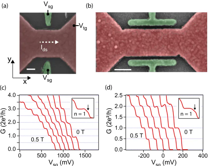
electrodes are finally defined using e-beam lithography and e-beam metal deposition: a central gate extending over the mesa is designed to induce the accumulation of a conducting hole channel between the source to the drain contact; two side gates, to be operated in depletion mode, create a tunable 1D constriction in the channel oriented along the [100] direction. We have varied the geometry of the side gates in order to explore gate-defined 1D hole wires with different lengths. Here we present experimental data for two devices, one with a short (∼ 100 nm) and one with a long (∼ 600 nm) constriction (see Figs. 1 (a) and (b), respectively).
All magnetotransport measurements were done at 270 mK in a 3He cryostat equipped
with a superconducting magnet. Figure 1 (c) shows a data set for a device, labelled D1, nominally identical to the one shown in Fig. 1 (a). The differential conductance, G, measured at dc source-drain bias voltage Vds = 0, is plotted as a function of Vsg for magnetic fields, ~B, perpendicular to the QW plane and varying from 0 to 0.5 T. In our experiment, G was directly measured using standard lock-in detection with a bias-voltage modulation δVsd = 10 µV at 36.666 Hz. In addition, G was numerically corrected to remove the contribution from all series resistances (∼ 20 kΩ), i.e. the resistances of the measurement circuit, the source and drain contacts, and the two-dimensional hole gas.
h is the Plank constant. This finding is consistent with the results of a recently published
independent work carried out on a similar SiGe heterostructure.26 Applying an out-of-plane
magnetic field lifts the spin degeneracy of the 1D subbands, resulting in plateaus at multiples of e2/h. These plateaus underpin the formation of spin-polarized subbands. They emerge
at relatively small magnetic fields, of the order of a few hundred mT, denoting a large out-of-plane g-factor as expected in the case of a predominant HH character.
We measured several devices with side-gate lengths, Lg, ranging from 100 nm (as in Fig. 1 (a)) to 900 nm. The G(Vsg) measurements shown in Fig. 1(d) were taken on a device with Lg ≈ 600 nm, labelled as D2 and nominally identical to the one shown in Fig. 1(b). Remarkably, these measurements demonstrate that clear conductance quantization can be observed also in relatively long channels largely exceeding 100 nm.
We note that a shoulder at G ∼ 0.7 × 2e2/h is visible in the B = 0 traces of both Fig.
1 (c) and (d). This feature, which is highlighted in the respective insets, corresponds to the so-called 0.7 anomaly. Discovered and widely studied in quantum point contacts defined in high-mobility two-dimensional electron systems,30–35 and more recently observed also in
semiconductor nanowires,36,37 the interpretation of this phenomenon remains somewhat
de-bated.38–42
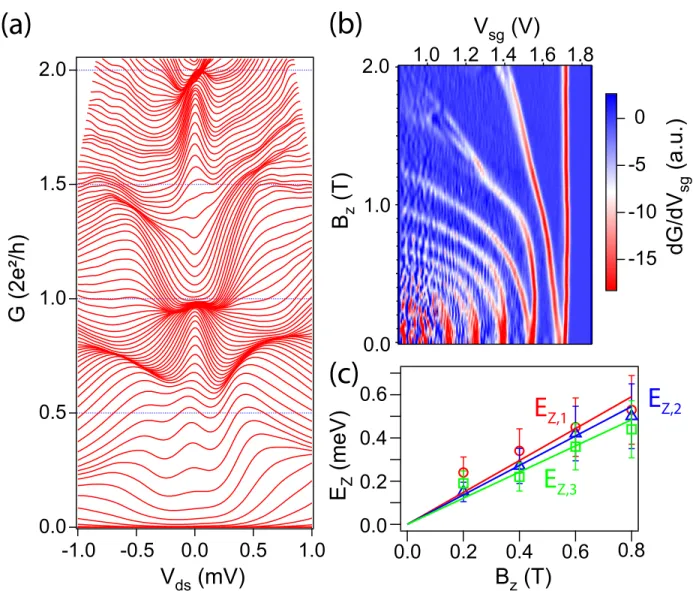
To further confirm the 1D nature of the observed conductance quantization, we present in Figs. 2 (a)-(c) waterfall plots of the non-linear G(Vds) at three different perpendicular magnetic fields (B = 0, 0.3, and 0.5 T, respectively) for device D1. Clear bunching of the G(Vds) is observed around Vds = 0 for gate voltages corresponding to the quantized conductance plateaus of Fig. 1(c). With magnetic field applied, the first plateau at G = e2/h
begins to appear at B = 0.3 T and is fully formed at B = 0.5 T. At B = 0, a zero-bias dI/dV peak can seen in correspondence of the 0.7 structure, in line with previous observations.33
The well-resolved spin splitting of the 1D subbands enables a quantitative study of the hole g-factors. To investigate the g-factor anisotropy, we applied ~B not only along the z axis, perpendicular to the substrate plane, but also along the in-plane directions x and y,
indicated in Figure 1 (a). To change the ~B direction, the sample had to be warmed up, rotated, and cooled down multiple times. Thermal cycling did not modify significantly the device behavior, except for the value of threshold voltage on the channel gate for the activation of hole conduction in the Ge QW (this voltage is sensitive to variations in the static charges on the sample surface).
Figures 3 (a), (b) and (c) show the B-evolution of the trans-conductance dG/dVsg as a function of Vsg, with ~B applied along x, y and z, respectively. The data refer to device D1. In these color maps, the blue regions, where dG/dVsg is largely suppressed, correspond to the plateaus of quantized conductance. On the other hand, the red ridges of enhanced
dG/dVsg correspond to the conductance steps between consecutive plateaus, which occur every time the edge of a 1D subband crosses the Fermi energy of the leads. At finite B, the red ridges split, following the emergence of new conductance plateaus at odd-integer multiples of e2/h. Upon increasing B, the splitting in Vsg increases proportionally to the
Zeeman energy EZ,n = |En,↑− En,↓|, where En,σ is the energy of the 1D subband with spin polarization σ and orbital index n.
For an in-plane B, either along x or y, the splitting becomes clearly visible only above approximately 2 T. As a result, the explored B range extends up to 6 T. For a perpendicular field, the Zeeman splitting is clearly more pronounced being visible already around 0.2 T. This apparent discrepancy reveals a pronounced g-factor anisotropy, with a g-factor along the z-axis, gz, much larger than the in-plane g-factors, gx and gy. Such a strong anisotropy is expected in the case of two-dimensional hole states with dominant HH character, corrob-orating the hypothesis of a dominant confinement in the z direction, which is imposed by the QW heterostructure.
Besides causing the Zeeman splitting of the 1D subbands, the applied ~B has an effect on the orbital degree freedom of the hole states. The effect is relatively weak in the case of an in-plane B because the magnetic length, inversely proportional to √B, gets as small as
contrary, the relatively weak lateral confinement imposed by the side gates leaves room for a pronounced B-induced orbital shift. This manifests in Fig. 3 (c) as an apparent bending of the dG/dVsg ridges towards more negative gate voltages.
In order to quantitatively estimate the observed Zeeman splittings, and the correspond-ing g-factors, we performed bias-spectroscopy measurements of dG/dVsg as a function of
Vds and Vsg at different magnetic fields. In these measurements, the dG/dVsg ridges form diamond-shape structures from which we extract the Zeeman energies, as well as the lever-arm parameters relating Vsg variations to energy variations. Representative dG/dVsg(Vds,Vsg) measurements, and a description of the well-known procedure for the data analysis are given in Supplementary Information. Interestingly, for a given B, both the Zeeman energy and the lever-arm parameter can vary appreciably from subband to subband.
Figures 3 (d), (e), and (f) present the estimated EZ,n values as a function of B, for the
first few subbands, and for the three B directions. Linear fitting to EZ,n = gnµBB yields
the Landé g-factors, gx,n, gy,n, and gz,nfor the three perpendicular directions. The extracted
g-factors for the device D1 are listed in Table 1. We have included also the gz,n values
obtained from another device (D3) with Lg = 100 nm.
For device D1 (D3), the perpendicular g-factor ranges between 12.0 (10.4) and 15.0 (12.7), while the in-plane one is much smaller, varying between 0.76 and 1.00, with no significant difference between x and y directions. A large in-plane/out-of-plane anisotropy in the g-factors is consistent with the hypothesis of a dominant HH character. In fact, in the limit of vanishing thickness, the lowest subbands of a Ge QW should approach pure HHs with
gx ≈ gy ≈ 0 and gz = 6κ + 27q/2 = 21.27, where κ and q are the Luttinger parameters (κ = 3.41 and q = 0.06 for Ge).
In the investigated SiGe QW heterostructure, the HH nature of the first 2D subbands is enhanced by the presence of a biaxial compressive strain in the Ge QW, increasing by ∼ 40 meV the energy splitting with the first light-hole (LH) subbands.43 The creation of a
dominated by the QW along the growth axis (z). From a measured energy spacing of around 0.65 meV between the first and the second 1D subband (see Supplementary Information), we estimate that the hole wavefunctions of the first subband have a lateral width (along
y) of approximately 80 nm, which is an order of magnitude larger than the wavefunction
extension along z.
The results summarized in Table 1 suggest a slight tendency of the g-factors to decrease with the subband index. This trend is consistent with the results of earlier experiments with both electron36,44 and hole45–47 quantum point contacts. A possible explanation is that the
exchange interaction increases the g-factor in the low-density limit.31,48 Yet hole g-factors in
quantum point contacts depend also on a complex interplay of spin-orbit coupling, applied magnetic field, and electrostatic potential landscape.49,50 Acquiring a deep understanding
of the g-factors reported here would require more extensive and sophisticated experiments together with a nontrivial theoretical analysis, which goes well beyond the scope of the present work.
In conclusion, we have demonstrated ballistic hole transports in 1D quantum wires gate-defined in a Ge/Si0.2Ge0.8 heterostructure. The ballistic regime is observed for wires up to
600 nm long. By investigating the Zeeman splitting of the quantized conductance steps we find that out-of-plane g-factors are an order of magnitude larger than the in-plane ones, denoting a pronounced HH character. This can be ascribed to the dominant confinement along the growth axis and to the compressive biaxial strain in the Ge QW. The observation of ballistic 1D hole transport in remarkably long channels and large out-of-plane g-factors holds special promise for the development of devices with spin-related functionality. In principle, the fabrication of these devices could be implemented in an industry-standard fab line with the possibility of monolithic integration with conventional silicon electronics.
Supplementary Information
Additional experimental data from a gated Hall-bar device, providing information of the transport properties of the two-dimensional hole gas. Additional data from another 1D-wire device (D3). Description of the procedure to extract energy spacings in a 1D channel.
Acknowledgement
We acknowledge financial support from the Agence Nationale de la Recherche, through the TOPONANO project.
References
(1) Awschalom, D. D.; Flatté, M. E. Nature Physics 2007, 3, 153.
(2) Nadj-Perge, S.; Pribiag, V. S.; van den Berg, J. W. G.; Zuo, K.; Plissard, S. R.; Bakkers, E. P. A. M.; Frolov, S. M.; Kouwenhoven, L. P. Phys. Rev. Lett. 2012, 108, 166801.
(3) Pribiag, V. S.; Nadj-Perge, S.; Frolov, S. M.; van den Berg, J. W. G.; van Weperen, I.; Plissard, S. R.; Bakkers, E. P. A. M.; Kouwenhoven, L. P. Nature Nanotechnology 2013,
8, 170.
(4) Gerardot, B. D.; Brunner, D.; Dalgarno, P. A.; Öhberg, P.; Seidl, S.; Kroner, M.; Kar-rai, K.; Stoltz, N. G.; Petroff, P. M.; Warburton, R. J. Nature 2008, 451, 441.
(5) Bulaev, D. V.; Loss, D. Phys. Rev. Lett. 2007, 98, 097202.
(6) Fischer, J.; Coish, W. A.; Bulaev, D. V.; Loss, D. Phys. Rev. B 2008, 78, 155329. (7) Maurand, R.; Jehl, X.; Kotekar-Patil, D.; Corna, A.; Bohuslavskyi, H.; Laviéville, R.;
Hutin, L.; Barraud, S.; Vinet, M.; Sanquer, M.; De Franceschi, S. Nature
Communica-tions 2016, 7, 13575.
(8) Ono, K.; Giavaras, G.; Tanamoto, T.; Ohguro, T.; Hu, X.; Nori, F. Phys. Rev. Lett.
2017, 119, 156802.
(9) Watzinger, H.; Kukučka, J.; Vukušić, L.; Gao, F.; Wang, T.; Schäffler, F.; Zhang, J.-J.; Katsaros, G. arXiv preprint arXiv:1802.00395 2018,
(10) De Franceschi, S.; Kouwenhoven, L.; Schönenberger, C.; Wernsdorfer, W. Nature
Nan-otechnology 2010, 5, 703.
(11) Clark, T. D.; Prance, R. J.; Grassie, A. D. C. Journal of Applied Physics 1980, 51, 2736–2743.
(12) de Lange, G.; van Heck, B.; Bruno, A.; van Woerkom, D. J.; Geresdi, A.; Plissard, S. R.; Bakkers, E. P. A. M.; Akhmerov, A. R.; DiCarlo, L. Phys. Rev. Lett. 2015, 115, 127002. (13) Casparis, L.; Larsen, T. W.; Olsen, M. S.; Kuemmeth, F.; Krogstrup, P.; Nygård, J.;
Petersson, K. D.; Marcus, C. M. Phys. Rev. Lett. 2016, 116, 150505.
(14) Lutchyn, R.; Bakkers, E.; Kouwenhoven, L.; Krogstrup, P.; Marcus, C.; Oreg, Y. arXiv
preprint arXiv:1707.04899 2017,
(15) Maier, F.; Klinovaja, J.; Loss, D. Phys. Rev. B 2014, 90, 195421.
(16) Lu, W.; Xiang, J.; Timko, B. P.; Wu, Y.; Lieber, C. M. Proceedings of the National
Academy of Sciences of the United States of America 2005, 102, 10046–10051.
(17) Kotekar-Patil, D.; Nguyen, B.-M.; Yoo, J.; Dayeh, S. A.; Frolov, S. M. Nanotechnology
2017, 28, 385204.
(18) Xiang, J.; Vidan, A.; Tinkham, M.; Westervelt, R. M.; Lieber, C. M. Nature
(19) Su, Z.; Zarassi, A.; Nguyen, B.-M.; Yoo, J.; Dayeh, S. A.; Frolov, S. M. arXiv preprint
arXiv:1610.03010 2016,
(20) Katsaros, G.; Golovach, V. N.; Spathis, P.; Ares, N.; Stoffel, M.; Fournel, F.; Schmidt, O. G.; Glazman, L. I.; De Franceschi, S. Phys. Rev. Lett. 2011, 107, 246601. (21) Ares, N.; Katsaros, G.; Golovach, V. N.; Zhang, J. J.; Prager, A.; Glazman, L. I.;
Schmidt, O. G.; Franceschi, S. D. Applied Physics Letters 2013, 103, 263113.
(22) Zhang, J. J.; Katsaros, G.; Montalenti, F.; Scopece, D.; Rezaev, R. O.; Mickel, C.; Rellinghaus, B.; Miglio, L.; De Franceschi, S.; Rastelli, A.; Schmidt, O. G. Phys. Rev.
Lett. 2012, 109, 085502.
(23) Myronov, M.; Morrison, C.; Halpin, J.; Rhead, S.; Casteleiro, C.; Foronda, J.; Shah, V. A.; Leadley, D. Japanese Journal of Applied Physics 2014, 53, 04EH02. (24) Shi, Q.; Zudov, M. A.; Morrison, C.; Myronov, M. Phys. Rev. B 2015, 91, 241303. (25) Laroche, D.; Huang, S.-H.; Chuang, Y.; Li, J.-Y.; Liu, C.; Lu, T. Applied Physics Letters
2016, 108, 233504.
(26) Gul, Y.; Holmes, S. N.; Newton, P. J.; Ellis, D. J. P.; Morrison, C.; Pepper, M.; Barnes, C. H. W.; Myronov, M. Applied Physics Letters 2017, 111, 233512.
(27) Gul, Y.; Holmes, S. N.; Myronov, M.; Kumar, S.; Pepper, M. Journal of Physics:
Condensed Matter 2018, 30, 09LT01.
(28) Hendrickx, N.; Franke, D.; Sammak, A.; Kouwenhoven, M.; Sabbagh, D.; Yeoh, L.; Li, R.; Tagliaferri, M.; Virgilio, M.; Capellini, G. arXiv preprint arXiv:1801.08869 2018, (29) Myronov, M.; Morrison, C.; Halpin, J.; Rhead, S.; Casteleiro, C.; Foronda, J.;
(30) van Wees, B. J.; van Houten, H.; Beenakker, C. W. J.; Williamson, J. G.; Kouwen-hoven, L. P.; van der Marel, D.; Foxon, C. T. Phys. Rev. Lett. 1988, 60, 848–850. (31) Thomas, K. J.; Nicholls, J. T.; Simmons, M. Y.; Pepper, M.; Mace, D. R.; Ritchie, D. A.
Phys. Rev. Lett. 1996, 77, 135–138.
(32) Kristensen, A.; Bruus, H.; Hansen, A. E.; Jensen, J. B.; Lindelof, P. E.; Marck-mann, C. J.; Nygård, J.; Sørensen, C. B.; Beuscher, F.; Forchel, A.; Michel, M. Phys.
Rev. B 2000, 62, 10950–10957.
(33) Cronenwett, S. M.; Lynch, H. J.; Goldhaber-Gordon, D.; Kouwenhoven, L. P.; Mar-cus, C. M.; Hirose, K.; Wingreen, N. S.; Umansky, V. Phys. Rev. Lett. 2002, 88, 226805. (34) Danneau, R.; Klochan, O.; Clarke, W. R.; Ho, L. H.; Micolich, A. P.; Simmons, M. Y.;
Hamilton, A. R.; Pepper, M.; Ritchie, D. A. Phys. Rev. Lett. 2008, 100, 016403.
(35) Komijani, Y.; Csontos, M.; Ihn, T.; Ensslin, K.; Meir, Y.; Reuter, D.; Wieck, A. D.
Phys. Rev. B 2013, 87, 245406.
(36) Heedt, S.; Prost, W.; Schubert, J.; Grützmacher, D.; Schäpers, T. Nano Letters 2016,
16, 3116–3123, PMID: 27104768.
(37) Saldaña, J.; Žitko, R.; Cleuziou, J.; Lee, E.; Zannier, V.; Ercolani, D.; Sorba, L.; Aguado, R.; De Franceschi, S. arXiv preprint arXiv:1801.01855 2018,
(38) Micolich, A. P.; Zülicke, U. Journal of Physics: Condensed Matter 2011, 23, 362201. (39) Iqbal, M. J.; Levy, R.; Koop, E. J.; Dekker, J. B.; de Jong, J. P.; van der Velde, J.
H. M.; Reuter, D.; Wieck, A. D.; Aguado, R.; Meir, Y.; van der Wal, C. H. Nature 2013,
501, 79.
(40) Bauer, F.; Heyder, J.; Schubert, E.; Borowsky, D.; Taubert, D.; Bruognolo, B.; Schuh, D.; Wegscheider, W.; von Delft, J.; Ludwig, S. Nature 2013, 501, 73.
(41) Brun, B.; Martins, F.; Faniel, S.; Hackens, B.; Bachelier, G.; Cavanna, A.; Ulysse, C.; Ouerghi, A.; Gennser, U.; Mailly, D.; Huant, S.; Bayot, V.; Sanquer, M.; Sellier, H.
Nature Communications 2014, 5, 4290.
(42) Iagallo, A.; Paradiso, N.; Roddaro, S.; Reichl, C.; Wegscheider, W.; Biasiol, G.; Sorba, L.; Beltram, F.; Heun, S. Nano Research 2015, 8, 948–956.
(43) Failla, M.; Myronov, M.; Morrison, C.; Leadley, D. R.; Lloyd-Hughes, J. Phys. Rev. B
2015, 92, 045303.
(44) Martin, T. P.; Szorkovszky, A.; Micolich, A. P.; Hamilton, A. R.; Marlow, C. A.; Linke, H.; Taylor, R. P.; Samuelson, L. Applied Physics Letters 2008, 93, 012105. (45) Daneshvar, A. J.; Ford, C. J. B.; Hamilton, A. R.; Simmons, M. Y.; Pepper, M.;
Ritchie, D. A. Phys. Rev. B 1997, 55, R13409–R13412.
(46) Danneau, R.; Klochan, O.; Clarke, W. R.; Ho, L. H.; Micolich, A. P.; Simmons, M. Y.; Hamilton, A. R.; Pepper, M.; Ritchie, D. A.; Zülicke, U. Phys. Rev. Lett. 2006, 97, 026403.
(47) Srinivasan, A.; Hudson, K. L.; Miserev, D.; Yeoh, L. A.; Klochan, O.; Muraki, K.; Hirayama, Y.; Sushkov, O. P.; Hamilton, A. R. Phys. Rev. B 2016, 94, 041406.
(48) Wang, C.-K.; Berggren, K.-F. Phys. Rev. B 1996, 54, R14257–R14260. (49) Miserev, D. S.; Sushkov, O. P. Phys. Rev. B 2017, 95, 085431.
(50) Miserev, D. S.; Srinivasan, A.; Tkachenko, O. A.; Tkachenko, V. A.; Farrer, I.; Ritchie, D. A.; Hamilton, A. R.; Sushkov, O. P. Phys. Rev. Lett. 2017, 119, 116803.
2.0 1.0 0.0 1.5 1.0 0.5 0.0
V
sg(V)
-15 -10 -5 0 5 dG/dVsg (a.u.)B
z(T)
200 nm
V
sgV
sgV
tgI
ds(a)
x
y
(b)
4.0 3.0 2.0 1.0 0.0 1500 1000 500 0 0 T 0.5 T 2.5 2.0 1.5 1.0 0.5 0.0 400 200 0 -200 0 T 0.5 T(c)
(d)
V
sg(mV)
G (2e²/h)
V
sg(mV)
G (2e²/h)
n = 1 n = 1Figure 1: (a) and (b) False color scanning electron micro-graphs of representative devices. Scale bars: 100 nm (a) and 200 nm (b). Gate voltages Vtg < 0 and Vsg > 0 are applied to
the channel gate (colorized in red) and the two side gates (colorized in green), respectively. Current Ids flows in Ge QW under the channel gate along the x direction. To enable that, the channel gate extends of all the way to the source/drain contact pads, which are located about 15 µm away from nanowire constriction, i.e. outside of the view field in (a) and (b). (c) and (d) Measurements of zero-bias conductance G as a function of Vsg at different perpendicular magnetic fields, Bz, from 0 to 0.5 T (step: 0.1 T). Data in (c) ((d)) refer to device D1 (D2), which is nominally identical to the one shown in (a) ((b)). In both cases we observe clear conductance quantization and the lifting of spin degeneracy at finite field. Conductance has been rescaled to remove the contribution of a series resistance RS slightly varying with Bz between 22 and 24 kΩ. The different traces are laterally offset for clarity. Insets: Zoom-in of the 0.7 anomaly (indicated by an arrow) at zero magnetic field.
(c)
(a)
(b)
V
ds(mV)
V
ds(mV)
3.0
2.5
2.0
1.5
1.0
0.5
0.0
G (2e²/h)
V
ds(mV)
-0.5
0.0
0.5
-0.5
0.0
0.5 -0.5
0.0
0.5
Figure 2: Waterfall plots of differential conductance, G, as a function of source-drain bias,
Vds, at different values of side-gate voltage Vsg (gate step: 5 mV). The three plots were taken
on device D1 at different out-of-plane magnetic fields: (a) 0 T, (b) 0.3 T and (c) 0.5 T. The spanned Vds range varies with Vsg, and hence with G. This follows from the procedure used to take into account the effect of the series resistance, RS. In this procedure, we assumed RS to be monotonically increasing with the current Isd flowing across the device. This assumption was motivated by the need to account for non-linearities in the series resistance coming primarily from the source/drain contacts to the two-dimensional hole gas. At Vsd = 0, RS is a constant all over the spanned Vsg range. At finite Vsd, RS varies with Vsg due to the Vsg dependence of G. As a result, the corrected Vds range tends to decrease when lowering Vsg, and hence increasing G.
2.0 1.0 0.0 1.5 1.0 0.5 0.0 Vsg (V) 6.0 4.0 2.0 0.0 Bx (T) 1.4 1.2 1.0 0.8 0.6 Vsg (V) 6.0 4.0 2.0 0.0 By (T) 1.2 1.0 0.8 0.6 0.4 Vsg (V) -15 -10 -5 0 5 dG/dV sg (a.u.) EZ (meV) Bz(T) Bx(T) By(T) (c) (a) (b) (f) (d) (e) EZ,2 EZ,1 EZ,3 EZ,2 EZ,1 EZ,3 EZ,2 EZ,1 Bz (T) 0.5 0.4 0.3 0.2 0.1 0.0 0.5 0.4 0.3 0.2 0.1 0.0 0.5 0.4 0.3 0.2 0.1 0.0 6.0 4.0 2.0 0.0 0.3 0.2 0.1 0.0 6.0 4.0 2.0 0.0 0.4
Figure 3: (a)-(c) Numerical derivative of G with respect to Vsg as a function of Vsg and magnetic field applied along the x (a), y (b) and z (c) directions (data from device D1). (d)-(f) Zeeman splittings EZ,n = |En,↑− En,↓|as a function of magnetic field along the x (d),
y(e) and z (f) directions. Red, blue, and green open symbols correspond to the first, second,
and third spin-split subbands, respectively. The g factors for each subband are obtained from the slope of the linear fits to the Zeeman relation EZ,n(B) (solid lines). The results are
Table 1: This table summarizes the results of g-factor measurements on device D1 and D3. These g-factors are obtained from the slope of the linear fits in Fig. 3 (d)-(f)) and Fig. S3 (c). g1 g2 g3 D1 Bx 1.00 ± 0.15 0.82 ± 0.12 -By 1.00 ± 0.15 0.91 ± 0.19 0.76 ± 0.16 Bz 15.0 ± 2.3 12.0 ± 1.8 13.0 ± 2.8 D3 Bz 12.7 ± 2.2 11.8 ± 1.8 10.4 ± 1.6
Supplementary materials: Ballistic one-dimensional hole
transport in Ge/SiGe heterostructure
Hall measurements
The details of the heterostructure used in the present work are given in Fig. S1 (a).S1,S2
To characterize the basic electronic properties of this heterostructure, gated Hall-bar devices (Fig. S1 (b)) were fabricated and measured at 0.3 K. Representative measurements of longitudinal resistivity, ρxx, and Hall resistance, ρxy, are shown in Fig. S1 (c). Shubnikov-de Haas (SdH) oscillations and quantum Hall plateaus are observed in ρxxand ρxy, , respectively. The two-dimensional hole density, ns, and the hole mobility, µ, are plotted as a function of
Vtg in Fig. S1 (d). In the shown Vtg range, ns depends linearly on Vtg, reaching the largest value of 0.8 × 1010cm−2 at the most negative Vtg. This is close to maximal hole density that
could be achieved. In fact, by going to more negative Vtg, i.e. Vtg < −4 V, we encountered
two types of problems: the accumulation of a parasite hole gas at the interface with the gate oxide,S3,S4 and gate leakage.
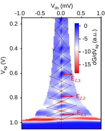
Measurement of the Zeeman energy
In this section we illustrate the procedure to measure Zeeman energy splittings. The color plot in Fig. S2 is a representative example of a dG/dVsg as a function of Vds and Vsg at Bz = 0.4 T. The magnetic field is large enough to lift spin degeneracy. The diamond-shape blue regions centered around Vds = 0 V correspond to conductance plateaus at integer multiples of e2/h. White/red lines bordering the diamonds define the edges of the plateaus.
These lines are not always clearly visible. Dashed lines have been drawn to highlight their position. These lines correspond to aligning the energy of a subband edge with the Fermi energy of either the source or the drain lead. As a result, the apexes of the diamonds, defined
by the crossings of consecutive dashed lines, are located at a source-drain bias voltage equal to the energy spacing between consecutive subband edges. The horizontal half-widths of the odd diamonds provide a direct quantitative measurement of the Zeeman energies EZ,n, as illustrated in Fig. S2. The measurement accuracy can be conservatively estimated by varying the slope of the dashed lines until it becomes apparent that they no longer follow the
dG/dVsg ridges. Because the dG/dVsg ridges happen to be generally broad and sometimes even hard to identify, we end up with rather large measurement uncertainties.
Besides providing access to the Zeeman splitting energies, the stability diagram of Fig. S2 can be used to extract the gate lever-arm parameter, α, which is the proportionality factor relating a gate voltage variation to the corresponding shift in the electrochemical potential in the 1D wire. In practice, for the n-th orbital subband α is obtained from the ratio between
EZ,n and the height (measured along the Vsg axis) of the 2n−1 diamond. We find that α decreases noticeably with n and, to a lower extent, it varies with ~B. For the case of Fig. S2 we find α ≈ 5 × 10⁻³eV /V for n = 1, α ≈ 3.3 × 10⁻³eV /V for n=2, and α ≈ 2.3 × 10⁻³eV /V
for n = 3.
In the limit of vanishing ~B, the odd diamonds shrink and disappear while the even diamonds grow. At B = 0, the 2n diamond has a horizontal half-width set by the energy spacing ∆n,n+1 between the n-th and the (n+1)-th orbital subband. We measure ∆1,2 ≈0.65
meV and ∆2,3 ≈0.5 meV.
Data from device D3
Figure S3 shows a set of data from a third device (D3) made from the same heterostruc-ture. This device has the same gate layout as D1 as shown in Fig. 1 (a) of the main text. It was measured with only one orientation of the applied magnetic field, perpendicular to the device plane (z-axis). The procedure to correct for the series resistances, and the data analy-sis was the same as for the previous devices. The results are qualitatively and quantitatively
similar to those from device D1.
References
[S1] Morrison, C.; Casteleiro, C.; Leadley, D. R.; Myronov, M. Applied Physics Letters 2016,
109, 102103
.
[S2] Myronov, M.; Morrison, C.; Halpin, J.; Rhead, S.; Foronda, J.; Leadley, D. Solid-State
Electronics 2015, 110, 35 – 39
.
[S3] Lu, T.; Lee, C.-H.; Huang, S.-H.; Tsui, D.; Liu, C. Applied Physics Letters 2011, 99, 153510
.
[S4] Huang, C.-T.; Li, J.-Y.; Chou, K. S.; Sturm, J. C. Applied Physics Letters 2014, 104, 243510
8 6 4 2 0 8 6 4 2 0 -2 -4 B (T) 40 20 0 -20 Si cap layer 2 nm Al2O3 oxide 30 nm Strained Ge QW 22 nm Ti/Au gate 30 nm Si0.2Ge0.8 spacer 72 nm Si0.2Ge0.8/Ge buffer ~2 µm Si(001) substrate (a) Vch VH Vtg Ich Vds Rserial Vtg (V) μ (10 5 cm 2/Vs) ns (10 11 cm -2) ρxx (k Ω /sq) 1.76 1.72 1.68 1.64 -4 -3 0.80 0.70 0.60 0.50 ρxy (k Ω ) (b) (c) (d) μ ns W L
Figure S1: (a) Schematic diagram of Ge/Si0.2Ge0.8heterostructure with top gate. (b) Optical
image of a gated Hall bar structure. White broken lines indicate six ohmic contacts. A top gate (yellow) overlaps each ohmic contacts and mesa structure. The mesa structure with a channel (L = 80 µm and W = 20 µm) is seen through the top gate. The channel direction is [¯110]. A serial resistance Rserial = 1 MΩ is connected to the channel. Constant bias voltage is applied and when the channel resistance is much lower than the Rserial a constant current flows. The current through the channel Ids, longitudinal voltage Vch and Hall voltage VH are measured at 300 mK as a function of gate voltage Vtg or out-of-plane magnetic field
B and converted to longitudinal sheet resistivity ρxx = Vch/Ids ∗ W/L and Hall resistivity
ρxy = VH/Ids. (c) Typical results of ρxx and ρxy vs B for Vds = 100 mV and Vtg = -4 V. Clear longitudinal resistivity oscillation (Shubnikov–de Haas effect) and Hall resistivity plateaus (quantum Hall effect) are observed (red and blue lines, respectively). At B = 3 T, the filling factor ν = 1. Around B = 5 T, ν = 2/3. (d) Hall density ns and hole mobility µ vs Vtg. ns is estimated from (classical) Hall effect in small magnetic fields and mobility µ is calculated for the relation µ = (ensρxx)−1 at B = 0, where e is the electron charge.
-1.0
-0.5
0.0
0.5
1.0
V
ds(mV)
0.2
0.4
0.6
0.8
1.0
0
-5
-10
-15
E
Z,1E
Z,2E
Z,3Figure S2: Color plot of dG/dVsg as a function of Vds and Vsg at B = 0.4 T. The spanned
Vds range varies with Vsg. The dashed lines highlight dG/dVsg ridges forming a sequence of diamond-shape regions. The odd diamonds form from the spin splitting of the 1D subbands. Their half-width gives the Zeeman energy as indicated by the horizontal arrows.
0.6
0.2
0.0
0.6
0.4
0.2
0.0
2.0
1.5
1.0
0.5
0.0
G (2e²/h)
-1.0 -0.5
0.0
0.5
1.0
V
ds(mV)
E
Z(meV)
B
z(T)
(a)
(c)
E
Z,1E
Z,3E
Z,22.0
1.0
0.0
B
z(T)
1.8
1.6
1.4
1.2
1.0
V
sg(V)
dG/dV
sg(a.u.)
-10
-5
0
(b)
-15
0.4
0.8
Figure S3: Experimental data for device D3. (a) Differential conductance G as a function of Vds at different Vsg and Bz = 0, (b) Linear transconductance dG/dVsg as a function of Vsg and Bz, and (c) Ez vs Bz. Large out-of-plane g factors are observed as in device D1 (see Table 1 in the main text).