HAL Id: hal-01022023
https://hal.inria.fr/hal-01022023
Submitted on 10 Jul 2014HAL is a multi-disciplinary open access archive for the deposit and dissemination of sci-entific research documents, whether they are pub-lished or not. The documents may come from teaching and research institutions in France or abroad, or from public or private research centers.
L’archive ouverte pluridisciplinaire HAL, est destinée au dépôt et à la diffusion de documents scientifiques de niveau recherche, publiés ou non, émanant des établissements d’enseignement et de recherche français ou étrangers, des laboratoires publics ou privés.
Self-Powered Conformable Deformation Sensor
Exploiting the Collective Piezoelectric Effect of
Self-Organised GaN Nanowires
Emmanuelle Pauliac-Vaujour, Sven Salomon, Joël Eymery, Edgar Leon Perez
To cite this version:
Emmanuelle Pauliac-Vaujour, Sven Salomon, Joël Eymery, Edgar Leon Perez. Self-Powered Con-formable Deformation Sensor Exploiting the Collective Piezoelectric Effect of Self-Organised GaN Nanowires. EWSHM - 7th European Workshop on Structural Health Monitoring, IFFSTTAR, Inria, Université de Nantes, Jul 2014, Nantes, France. �hal-01022023�
S
ELF
-
POWERED CONFORMABLE DEFORMATION SENSOR EXPLOITING
THE COLLECTIVE PIEZOELECTRIC EFFECT OF SELF
-
ORGANIZED
G
A
N
NANOWIRES
Emmanuelle Pauliac-Vaujour1
, Sven Salomon1
, Joël Eymery2
, Edgar Leon Perez1
1 CEA, LETI, 17 rue des martyrs, 38054 Grenoble Cedex 9, France. 2
CEA, INAC, 17 rue des martyrs, 38054 Grenoble Cedex 9, France.
emmanuelle.pauliac-vaujour@cea.fr
ABSTRACT
We present a novel integration-driven approach to the design of scale multi-physics sensors and systems. We implement this method to model, design, fabricate and characterize a thin, conformable low-cost impact detection sensor based on assemblies of piezoelectric GaN nanowires. When suitably assembled, the latter demonstrate a macroscale additivity of their nanoscale intrinsic properties, which enables to appeal to classical fabrication techniques and exploitable electronic readouts at the system level. We also exploit multi-level simulations to provide useful insights of adapted application-driven integration solutions for these new forms of sensors. We demonstrate the potential of such application-targeted, fully-integrated and modular systems to accommodate to the stringent requirements of structural health monitoring (SHM).
KEYWORDS : system integration, piezoelectric GaN wires, flexible sensor, finite
element modeling, impact detection.
INTRODUCTION
Considerable research effort is put towards the integration of new electronic functionalities in everyday-life objects. In the case of structural health monitoring (SHM), stringent requirements for a life-long monitoring of the degradations of large structures have emerged and broadly been discussed by the SHM community in terms of security enhancement and maintenance optimization over the past decade [1][2]. From the point of view of application fields, civil engineering and aeronautics were the first two domains to get a glimpse of the possible benefits and technological challenges of SHM in terms of long time, large scale, in-situ monitoring of ageing structures. Appeal for such solutions is now gradually spreading to other fields such as railway transport, energy infrastructures or the preserving of natural edifices.
From the R&D point of view, current SHM solutions encompass a variety of transducers among which the most represented ones are optical fiber-based sensors [4], piezoelectric sensors [5] and magnetic sensors [6]. For all categories of transducers, the main challenges associated with SHM are firstly (i) to develop sensors and actuators with suitable sensitivity, stability, robustness, dimensions and mechanical properties to be integrated at the heart of structures whose structural integrity must not be impaired and secondly, (ii) to implement this variety of distributed transducers over large scales following a well-managed network configuration, along with both local and deported processing of the information, communication means and a suitable energy consumption and management routine. These issues refer to “integration” both at the (i) sensor and (ii) system scales. The emergence of new forms of integrated functions and electronics is conditioned both by the physics of the system and the application. Nanotechnologies, in particular, demonstrate a great
potential both in terms of new functions and of new integration solutions. Indeed, the emergence of nanotechnology-based systems and nanoelectronics opens up new paths for innovative and robust integration solutions through dedicated system architectures that are “invisible” at the level of the instrumented structure while still enabling reliable, highly sensitive, multi-scale and massively distributed sensing and/or actuating functionalities prone to answer SHM stringent requirements.
In the present work, we focus on a technology of ultra-thin, flexible piezoelectric sensor which tackles the abovementioned issues through an original integration-driven approach. We have designed and fabricated a new conformable impact detection nanosensor based on assemblies of piezoelectric GaN wires. The wires are self-organized in humid phase, a low cost and high throughput process which is compatible with most organic and inorganic materials (ambient temperature and pressure). Conformability is obtained due to the loose mechanical constraints between adjacent wires encapsulated into a polymer medium. The macroscale piezoelectric effect is obtained by additivity of the elementary nanoscale effects. Consequently, deformations can be detected over a very large range of amplitudes thanks to a multi-scale texturing and a very high sensitivity (generated potential in the mV to V range). The sensor design can be modulated “at will” to obtain 1D, 2D or 3D macrostructures with an integrated piezoelectric (deformation sensing) function. The present paper does not give details of the associated electronics integration as this is still on-going research and will be the subject of further publication.
The originality of our approach lies in that the system architecture and design parameters were initially determined through multi-physics, application-driven models [7]. Based on these models, elementary nano-devices exhibiting macroscale piezo-responses were achieved. Through these devices, we validated the concept of very promising microscale-resolution sub-microscale-sensitivity strain sensors, whose particularity is to appeal to classical electronics and packaging solutions, despite the nanoscale dimensions of their active components. Complex application-dedicated system architectures of interconnected flexible arrays of self-activated piezoelectric sensors can be directly derived from the abovementioned multi-scale multi-level simulation-based procedure, echoing the need in SHM for adjustable, adaptable, low-complexity solutions.
1 MATERIALS AND METHODS
1.1 GaN wire synthesis and assembly
Ultra-long self-organized GaN wires with hexagonal sections were grown on sapphire substrates by catalyst-free metal-organic vapor phase epitaxy (MOVPE) [8][9]. The wire growth direction is along the (–c)-axis, which corresponds to the principal spontaneous piezoelectric polarization axis of the wurtzite structure. These self-organized and non-catalyzed wires have an average conical semi-angle of 0.3° with {1-100} sidewall facets. Their measured characteristic length was 120 ± 50 µm for a 0.8 µm average radius (Fig. 1a). The wire shape can span hexagonal with constant diameters to conical geometries by adjusting growth conditions such as doping concentration (from 5.1019
to 5.1020
atoms/cm3
), temperature and carrier gas pressure.
106 GaN wires/mL were dispersed in a solution of isooctane and 2-propanol (3:1 v/v ratio)
containing 50 µL of 5 mM 1-octadecylamine in hexane per 1 mL of suspension. Upon 12h incubation wires were rinsed 3 times with a clear isooctane / 2-propanol solution (3:1 v/v ratio) to remove the surfactant excess. These hydrophobic wires were then drop-spread on the water surface of a Langmuir-Blodgett (LB) trough Kibron Microtrough XS. After allowing the solvent to evaporate for 45 min, the Teflon barriers of the trough were compressed at 10 mm/min. Once a surface pressure of 35 mN/m was reached, the substrate was lifted at 1.5 mm/min to complete the LB assembly process (Fig. 1b). A densely-packed monolayer of well-aligned wires was obtained as shown in the inset of figure 1b.
EWSHM 2014 - Nantes, France
Figure 1: (a) SEM image of MOVPE GaN wires sonicated in isopropanol and deposited onto a Si substrate. The inset shows evidence of the wire conical shapes. (b) The Langmuir-Blodgett method to assemble wires.
The inset shows an SEM image of a compact monolayer of GaN wires obtained with this method. (c) Schematic of the wire-based sensor stacking and (d) photograph of a processed flexible device. 1.2 Sensor fabrication
The sensor was assembled (Fig. 1c) on a 125 µm flexible polyethylene naphthalate (PEN) film, previously coated with a Ti (20 nm) / Al (90 nm) electrode and with an insulating 1 µm thick parylene-C layer, a controlled and chemically stable dielectric (ɛr ~ 3.15) with a low leakage. Both metals and parylene-C were deposited by evaporation. Following the wire monolayer LB deposition, another 4µm thick conformal and pinhole free parylene-C layer was evaporated in vacuum at ambient temperature. Finally, the top Ti (20 nm) / Al (90 nm) electrode was deposited. The resulting sensor is equivalent to a parallel plate capacitor with a dielectric medium made of aligned wires and parylene-C. An example of a processed device is pictured in figure 1d. Both the thickness of the parylene-C and the compacity / ordering of the wire layer are critical parameters that were optimized through finite element (FEM) simulations as described in section 3.
2 ELECTRICAL MEASUREMENTS OF BENT PIEZOELECTRIC SENSORS
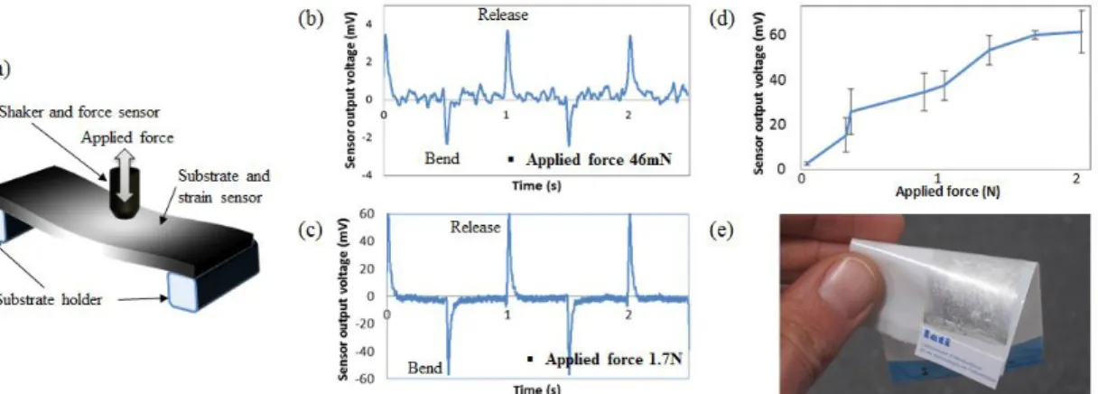
Prior to electrical measurements the flexible sensor was glued onto a 0.5 mm plastic substrate covered with a 3M scotch weld DP190 structural adhesive. This substrate was then fixed at its two ends to a substrate holder. A shaker was used to actuate the sensor by imposing a square or sinusoidal bending/release motion to the substrate (Fig. 2a). The applied force was measured by placing a calibrated force sensor at the shaker/sample interface. The correlation between the measured potentials and the wire strain was not straightforward. We monitored the substrate curvature induced by the shaker head displacement, but interface strain losses probably occur in the adhesive layer due to shear and decouple substrate strains from sensed strains [11]. Thus here, for accuracy, we deduce sensitivity with respect to the applied force and not to the induced strains or stresses. This device / structure interfacing is of crucial importance within the frame of in-situ SHM and will be discussed again in the conclusions.
The electrical modeling of the sensor can be viewed in a first approximation as a voltage source in serial connection with a capacitor. The impedance of the measurement probe is assumed to be purely resistive considering the actuation frequencies (in the Hz range) and is used as the charge load. The overall equivalent electric circuit is therefore equivalent to a high pass RC circuit.
The piezoelectric charges which are generated at the capacitor electrodes are screened by the motion of opposite charges across the resistive load: once the strain is released, the polarization vanishes and the excess charges of the capacitor flow back through the resistive load. In these measurements, the capacitance of the piezoelectric sensors (1.5 nF) and the 10 MΩ resistive load of the measurement probe lead to a system cutoff frequency of about 10 Hz. The sensor was consequently actuated with a square signal between 1 and 10 Hz to minimize signal attenuation by the measurement system. Using the above mentioned configuration, we were able to measure applied actuation forces on the substrate’s backplane in a 3 point configuration ranging from 46 mN up to 2.3 N for corresponding piezoelectric potentials of 4 to 80 mV respectively (Fig. 2b to d). Although it is possible to bend the device with curvature radii down to a few mm (Fig. 2e), for this experiment we could not impose displacements that induced forces greater than 2.3 N due to technical limitations related to the shaker. This corresponds to a radius of curvature of roughly 10 cm. In any case, such radii of curvature would not have been achievable with conventional piezoceramic materials.
Figure 2: (a) Bend/release actuation of the substrate in a 3 point configuration. Sensor piezoelectric output voltage when applying a square actuation force of (b) 46 mN and (c) 1.7 N on a 20 mm2
surface area of the 1.5 cm2
sensor active area. (d) Evolution of the maximum piezoelectric voltage drop as a function of the applied force. (e) Photograph of a self-standing bent device.
In these conditions, we were well below the elasticity limit of the substrate material and were not concerned by irreversible plastic deformation and sensor delamination from the substrate. We also took care that the shaker head was not electrostatically charged prior to actuation to avoid capacitive charge pumping. Opposite signals were measured when switching the sensor’s connection to the measurement system from a forward mode to a reverse mode or when switching from traction to compression, which is a clear signature of piezoelectric signals. However we observed some dispersion regarding the sensor sensitivities when measuring series of similarly fabricated devices. Maximal measured piezoelectric potentials ranged from tenths of mV to hundreds of mV when applying an actuating force around 2.3N. We will use finite element method (FEM) simulations below to demonstrate that this performance variability can be mainly attributed to wire orientation defects and overlapping inherent to the LB assembly process and is thus prone to further optimization.
3 FINITE ELEMENT MODELING
3.1 Theoretical considerations
The piezoelectric potential profiles in cylindrical nanowires induced by bending or uniaxial compression have been extensively studied using analytical or FEM models [12][13][14]. The
EWSHM 2014 - Nantes, France
potential distribution in the nanowire is usually derived by solving the Poisson equation assuming that there are no free carriers and that there are no surface residual charges. In our system, supposing no shear between the wire and parylene in a first approximation, we assume that uniaxial tensile/compressive deformations are dominant with respect to bending. The measurement of mechanical shear losses at the wire/dielectric interface is not straightforward and is the object of further investigation.
Figure 3: (a) Schematic of a conical wire lying on a flat surface submitted to a tensile force (b) Wire positioning within the simulated unit cell: a facet is parallel to the bottom electrode and lies in the y = 1 µm plane. (b) Simulated unit cell consisting of two aligned wires with opposite crystallographic (-c)-axes. Wires
are submitted to a tensile strain when the force F is applied at the edge of the unit cell.
Considering a tilted cone exhibiting a very small semi-angle α (Fig. 3a) with one edge parallel to the z axis, the longitudinal piezoelectric polarization vector can be projected on the y and z axes [15] and rewritten as:
y P
z PP z'sin z'cos . (3)
where z’ is collinear to the (-c)-axis. Equation (3) shows that a polarization along the y axis (i.e. normal to the electrodes) results from tilting the wire by its semi angle . At small values of α, this polarization can be approximated as proportional to . In this study, we focus on modeling the coupling between adjacent wires with opposite c-axis directions, i.e. in the unfavorable configuration where the contributions along the z axis exactly cancel each other while the smaller contributions along the y axis are additive.
In a first approximation, FEM calculations will neglect the spontaneous polarization of the wires [15]. Indeed, long GaN wires exhibit polar charges on their bottom and top ±(0001) planes, which can be considered as punctual and easily screened by foreign adsorbed molecules. Moreover, we can consider that this static electric field does not contribute significantly to the charge generation mechanism relying on dynamic carrier displacements at the capacitor electrodes. Considering the large dimensions of our GaN nanowires, we take their piezoelectric coefficients to be those of the bulk material: e33 = 0.73 C.m
-2
and e31 = e15 = -0.49 C.m -2
[16].
We study a configuration with coupled wires (maximum radius 0.8 µm, α=0.3°) lying flat in the y = 1 µm plane (Fig. 3b) with opposite (-c)-axes and separated by 8 µm (Fig. 3c). These wires are embedded in a dielectric material, which is sandwiched between two electrodes. The first electrode in the y = 0 plane is being grounded while the second is set at a floating potential. We choose a Parylene-C dielectric material and a PEN substrate, which we assume isotropic with Young moduli of 3 GPa and Poisson ratios of 0.4. Shear or glitches at the wire/dielectric interface cannot be taken into account with this simple FEM approach. This unit cell is the most representative configuration after assembling the wires via a LB process, where ±c axis are randomly organized.
3.2 Sensor performance optimization through technological parameter tuning
We first studied the influence of several technological parameters such as the parylene-C thickness (t), wire density, ordering or conical semi-angle (α) using FEM COMSOL® Multiphysics software. According to equation (3), α can tune the equivalent polarization amplitude along the thickness of the device. A parametric study shows that the piezopotential increases nearly linearly when increasing α. This result is in agreement with existing simulations [17] and confirms the importance of conicity in collecting a direct piezoelectric effect in assemblies of randomly aligned wires. This also indicates that a significant improvement of the sensor performances should be obtained by increasing this angle using optimized wire growth conditions.
The influence of the parylene-C thickness t was investigated as shown in figure 4a while keeping fixed the y = 1 µm bottom plane of the wires. Interestingly, the piezo-potential shows a maximum value for a 5µm total parylene-C thickness, independently of the applied deformation. Moreover, the piezo-potential amplitude is decreased by 50 % for t < 3.1 µm or t > 7.7 µm. The occurrence of this maximum can probably be attributed to the coupling between the wires and the electrode. Indeed, when strained along their (-c)-axis, positive and negative electric potentials are induced across the wires. If t is small, the individual effects of both potentials can be seen by the floating electrode and they tend to cancel each other out, while for large thicknesses both potentials are screened by the dielectric layer. An optimum is reached when wire coupling and dielectric screening balance each other. So this simulation shows how deposition process variations can drastically alter the sensor performances.
We then investigated the influence of the “assembly” parameters. As expected, the simulated output piezo-potential is proportional to the number of wires per unit cell. More interestingly, the LB assembly process may lead to some misaligned subdomains with angles ranging typically from 0° to 45° with respect to the strain direction. According to the simulations, the piezo-potential is maximal when the wires are aligned parallel to the strain direction as it maximizes the strain along their (±c)-axes (Fig. 4b). However it decreases by half when the angle between the wire and the strain direction reaches 30°. Wire overlapping may be another source of device performance variability and occurs during LB assembly when the surface pressure during deposition exceeds a threshold value of about 50 mN/m. Overlapping modifies the position of the wire in the dielectric layer and consequently changes the wire piezoelectric polarization along the y-axis (see equation 3). Hence, these calculations demonstrate the interest of using the LB technique to controllably assemble the wires into dense and well-aligned monolayers.
Figure 4: (a) Variation of the piezoelectric potential between ground and floating electrode as a function of the parylene-C thickness for different values of the applied force F (0.01-0.06N). (b) Normalized piezopotential as a function of the wire orientation β with respect to the strain direction. The potential was
normalized with respect to its maximal value since the unit cell width was enlarged to perform the wire rotations. The inset arrow depicts the main strain direction. F = 0.06N, t = 5 µm.
3.3 Extraction of sensor design information
Such simulations provide a valuable insight into the sensor design and integration architecture. Indeed, depending on the modes of solicitation of the sensor or network of sensors, technological
EWSHM 2014 - Nantes, France
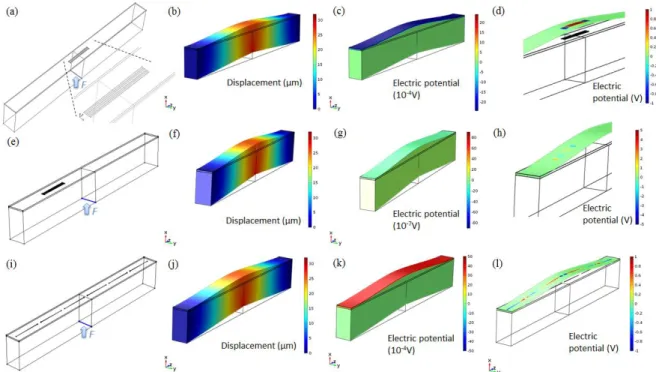
parameters and wire/electrode layouts may be tuned to yield the theoretically-best-suited sensor configuration. For example, we simulated an elementary 6-nanowire sensor on the surface of a PEN planar structure clamped at its two ends and which undergoes a deformation in the middle of its non-instrumented side (impact detection configuration). The piezo-potential profile in the wires and that collected in the top electrode were calculated as a function of the sensor design and location: a compact 2D patch in the center of the unit cell (Fig. 5a-d), off the center of the unit cell (Fig. 5e-h) and a 1D line of distributed wires (Fig. 5e-h). In all cases, wires are parallel with random (±c)-axis orientations as previously. The collected potentials on the top electrode were respectively 2.4mV, -5.10-7
mV and +4.2mV. The change of sign in the last case is a function of the wire arrangement and is being investigated further to determinate its predictability. Importantly, these simulations show that a continuous instrumentation (1D line) of the surface may be beneficial for this type of impact detection because it gets rid of the uncertainty associated with distributed sensor location (2D patch). Indeed in the case where the wires are located at an inflection point (Fig. 5h) and wires are randomly oriented, generated potentials may cancel each other out.
Figure 5: From left to right: schematic, deformation profile, potential distribution in top electrode and potential distribution in the plane of the nanowires for 3 configurations of sensor, placed on the top surface of
the PEN structure. An F = 0.06 N force is applied on the back and in the middle of the structure, which is clamped at both extremities. (a-d) Sensor in a 2D patch configuration, centered above the applied deformation, with randomly oriented parallel wires separated by 2.8 µm each. (e-h) Same as before with a patch off-centered by 215 µm. (i-l) Sensor in a line (1D) configuration with randomly oriented parallel wires separated by 20 µm each. Unit cell geometry: length 860 µm, width 65 µm, PEN thickness 125 µm, t = 5 µm.
CONCLUSIONS AND PERSPECTIVES WITH REGARDS TO SHM
We have investigated a new technology of thin, flexible deformation sensor based on a collective piezoelectric property of assemblies of GaN nanowires. We demonstrated the impact of technological parameters (material stack, wire and assembly characteristics) on the performance of the device. We implemented a multi-physics, multi-scale model which allows to accommodate the device design to the targeted application and the associated modes of solicitation. Further investigation is under way to quantify the robustness of the sensor, the losses at the structure/sensor interface depending on the way the sensor is integrated on/into the structure, and to implement different configurations of sensors (networks of patches, meshes, distributed electrodes, etc.) based
on real-condition simulations. Work on the electronics integration issues is also on-going. Importantly, the sensor-dimensioning approach presented in this article is very promising in order to adapt the characteristics of the sensor technology and system architecture to specific application constraints. It confers a high transferability and modularity to this technology, which is why we believe it has a strong potential for fully-integrated SHM.
ACKNOWLEDGMENTS
Authors acknowledge financial support from CEA’s Nanoscience Transversal Program.
REFERENCES
[1] V. Giurgiutiu, A. Zagrai, J.J. Bao, J.M. Redmond, D. Roach, K. Rackow, “Active sensors for health monitoring of aging aerospace structures”, International Journal of COMADEM 6 (1), pp. 3-21 (2003). [2] V. Giurgiutiu, A. Cuc, “Embedded non-destructive evaluation for structural health monitoring, damage
detection, and failure prevention”, The Shock and Vibration Digest 37 (2), pp. 83-105 (2005).
[3] D. Balageas, “Introduction au contrôle de santé intégré”, Revue de l’Electricité et de l’Electronique 2, pp. 31-40 (2006).
[4] M. Turpin, “Capteurs à fibres optiques. Quelles solutions pour la mesure en aéronautique ?”, Revue de
l’Electricité et de l’Electronique 2, pp. 47-53 (2006).
[5] P. Guy, T. Monnier, “Contrôle de santé des structures à l’aide de capteurs piézoélectriques”, Revue de
l’Electricité et de l’Electronique 2, pp. 41-46 (2006).
[6] M. Lemistre, D. Placko, “Les methodes électromagnétiques”, Revue de l’Electricité et de l’Electronique
2, pp. 54-60 (2006).
[7] R. Hinchet, J. Ferreira, J. Keraudy, G. Ardila, E. Pauliac-Vaujour, M. Mouis, L. Montes, “Scaling rules of piezoelectric nanowires in view of sensor and energy harvester integration”, IEEE International
Electron Devices Meeting IEDM (2012).
[8] R. Koester, J.S. Hwang, C. Durand, D. Le Si Dang, J. Eymery, “Self-assembled growth of catalyst-free GaN wires by metal-organic vapour phase epitaxy”, Nanotechnology 21, pp. 015602 (2010).
[9] J. Eymery, X. Chen, C. Durand, M. Kolb, G. Richter, “Self-organized and self-catalyst growth of semiconductor and metal wires by vapour phase epitaxy: GaN rods versus Cu whiskers”,
Comptes-Rendus de Physique 14, pp.221-227 (2013).
[10] G. Zhu, Y. Zhou, S. Wang, R. Yang, Y. Ding, X. Wang, Y. Bando, Z.L. Wang, “Synthesis of vertically aligned ultra-long ZnO nanowires on heterogeneous substrates with catalyst at the root”, Nanotechnology
23, pp. 055604 (2012).
[11] H. Cheng, J. Wu, M. Li, D.H. Kim, Y.S. Kim, Y Huang, Z. Kang, K.C. Hwang, J.A. Rogers, “An analytical model of strain isolation for stretchable and flexible electronics”, Applied Physics Letters 98, pp. 061902-3 (2011).
[12] Y. Gao, Z.L. Wang, “Electrostatic potential in a bent piezoelectric nanowire. The fundamental theory of nanogenerator and nanopiezotronics”, Nano Letters 7, pp. 2499-2505 (2007).
[13] G. Romano, G. Mantini, A.D. Carlo, A. D’Amico, C. Falconi, Z.L. Wang, “Piezoelectric potential in vertically aligned nanowires for high output nanogenerators”, Nanotechnology 22, pp. 465401 (2011). [14] R. Araneo, C. Falconi, “Lateral bending of tapered piezo-semiconductive nanostructures for
ultra-sensitive mechanical force to voltage conversion”, Nanotechnology 24, pp. 265707 (2013).
[15] Z.L. Wang, “Piezopotential in wurtzite semiconductors”, Piezotronics and Piezo-Photronics, Springer
Berlin Heidelberg, pp. 19-50 (2012).
[16] M. Minary-Jolandan, R.A. Bernal, I. Kuljanishvili, V. Parpoil, H.D. Espinosa, “Individual GaN nanowires exhibit strong piezoelectricity in 3D”, Nano Letters 12, pp.970-976 (2011).
[17] Y. Hu, Y. Zhang, C. Xu, G. Zhu, Z.L. Wang, “High-output nanogenerator by rational unipolar assembly of conical nanowires and its application for driving a small liquid crystal display”, Nano Letters 10, pp. 5025-5031 (2010).
EWSHM 2014 - Nantes, France