Commercialization of Silicon on Lattice-Engineered Substrate
for Electronic Applications
by
Yu Yan Liang
B.Eng, Materials Engineering (2007)
Nanyang Technological University, Singapore
Submitted to the Department of Materials Science and Engineering
in Partial Fulfilment of the Requirements for the Degree of
Master.of Engineering in Materials Science and Engineering
at the
Massachusetts Institute of Technology
September 2008
@2008 Massachusetts Institute of Technology.
All rights reserved.
Signature of Author:
Department of'Materials Scence and Engineering
Aug~st 8, 2008
Certified by:
•
Eug~JhfA. Fitiggrald
Merton C. Flemings-SMA Professor of Materials Science and Engineering
Thesis Supervisor
Accepted by:Samuel M. Allen
POSCO Professor of Physical Metallurgy
Chair, Departmental Committee for Graduate Students
Commercialization of Silicon on Lattice-Engineered Substrate
for Electronic Applications
by
Yu Yan Liang
Submitted to the Department of Materials Science and Engineering
on August 8, 2008 in Partial Fulfilment of
the Requirements for the Degree of
Master of Engineering in Materials Science and Engineering
Abstract
The commercial potential of SOLES (Silicon on Lattice-Engineered Substrate) is
investigated considering the competing technologies, competing market players and
market demands. Monolithic integration of Si devices with III-V electronic devices using
SOLES could be used to produce single chip wireless IC, catering the need of the most
prosperous consumer markets, the mobile phone market and the WLAN/WMAN/WWAN
wireless connectivity market. A cost model has been developed to justify the cost
effectiveness of single chip wireless IC. The commercial viability of SOLES is
commented based on these analyses.
Thesis Supervisor: Eugene A. Fitzgerald
Acknowledgement
A journey is easier when you travel together. I am lucky to have so many people
around me, accompanying me throughout this journey. I would like to take this
opportunity to thank the following for making my journey less lonely.
Foremost, I would like to thank my thesis advisor, Prof. Eugene Fitzgerald. I can
see that he is busy, but he always manages to squeeze a little time for me out of his
fully-occupied schedule. I am really impressed by his technopreneurial insights. His guidance
did help to deepen my understanding in this field. I would never forget his humour and
his charismatic speech, which make every discussion so enjoyable.
I would also like to thank Prof Yoon Soon Fatt, my PhD supervisor. He might not
realize his contributions to this master thesis. In fact, I received abundant help from
members in Prof Yoon's research group. Kah Pin, Tien Khee, Hendrix, Kim Luong,
Andrew and the group were always there for me whenever I had doubts. I owe them lots
of gratitude. And once again, thanks to Prof Yoon for introducing them to me.
I would like to thank Carl Dohrman, for introducing the SOLES technology to me
during the early stage of my thesis. And I would like to specially thank Prof Samudra. All
the professors from NTU and NUS dumped my email into their spam folder. Prof.
Samudra is the only one who replied me. His consultation was really helpful for me to
develop the cost model. Besides, I would like to thank Mr. Anuj from Marvell. He could
have ignored me, but he didn't. He helped to collect information from his colleagues,
who know a lot about the wireless industry.
Thanks to Zhoujia and Raghavan, my SMA course mates, as well as Rong Sheng,
my senior in NTU. They helped me a lot in my thesis work. They worked as my
dictionary and helped me in understanding the semiconductor jargon.
I wish to express my sincere gratitude to my SMA buddies, especially the
Ashdown study group members, Fidelia, Song Yang, Luo Jia, and Ha. Their presence
lived up my study life in MIT, warmed up the freezing winter in Cambridge. The fun and
joyous days with them makes my short stay at MIT so memorable. SMA is really a great
program. Other than financial support and precious learning experiences, it also offers
friendship. Thank you, SMA.
Last but not least, I would like to thank my daddy, mummy and my three young
and pretty sisters. You stand by me, and I stand tall. I cherish for having such a wonderful
family.
Table of Contents
Abstract ...
... 2
Acknowledgem ent ...
... 3
Table of Contents ... ... ... 5
List of Tables ...
6
List of Figures ...
7
Introduction ... 8
Technology Descriptions ...
... 10
Competing Technologies ... ... 14
Potential Applications ...
... 22
Supply Chain Analysis... ... 28
Cost Analysis ...
... 32
Business Strategy ... 36
Conclusions...
... 38
References...
... 40
Appendix 1 Relevant Patents ... ... 41
Appendix 2 Suppliers in Wireless IC Chip Supply Chain...
... 56
List of Figures
Figure 1 The projected growth of total processed compound semiconductor wafer area
up to year 2012 ...
...
8
Figure 2
Schematic drawing of SOLES. ...
... 10
Figure 3
Fabrication steps of SOLES ...
... 11
Figure 4
Schematic of monolithic integration achieved using the SOLES substrate... 12
Figure 5
Milestone for III-V devices on SiGe/Si platform...
13
Figure 6
Thermal expansion coefficient vs. lattice constant for semiconductors. ... 15
Figure 7
Comparison of four monolithic integration solutions ... 20
Figure 8
Mobile phone block diagram. ...
... 25
Figure 9
Range of powers and frequencies for wireless applications. ... 27
Figure 10 Worldwide WiFi chip market share in 2006 ...
29
Figure 11 Supply Chain of Wireless IC. ...
... 30
List of Tables
Table 1
List of patents regarding direct growth of III-V on Si... 14
Table 2
List of patents regarding direct growth of Ge on Si ...
...
16
Table 3
List of patents regarding compositional graded SiGe growth techniques. .... 17
Table 4
List of patents regarding Ge on Si through wafer bonding techniques... 18
Table
5
List of patents regarding growth of III-V on Ge ... . 18
Table 6
List of patents related to fabrication of SOLES...
.. 19
Table 7
List of patents regarding III-V on Si monolithic integration architectures.... 19
Table 8
Mobile phone chip makers ...
....
... 29
Table 9
Com parison of wafer cost ...
33
Table 10
Cost model comparing unit cost of IC chip in discrete packages and IC chip
Introduction
Silicon dominates the semiconductor market due to its economies of scale and high integration density of CMOS circuitry. Digital processing circuitry made of silicon has low power consumption. These advantages make silicon an excellent choice for high density low power consumption digital circuitry. Compound semiconductors are relatively new materials in semiconductor industry. They come into play by offering some unique properties which silicon could never outperform them, for examples, light emitting properties, high electron mobility and excellent performance for high speed high power applications. Both silicon and compound semiconductors play their significant roles that could hardly be taken over by one another. This turns out to be the driving force of heterointegration in the world of microelectronics.
Figure 1 The projected growth of total processed compound semiconductor wafer area up to year 2012 (Source: Compound Semiconductor Materials Report, Yole DNveloppement).
According to "Compound Semiconductor Materials Report" released in March 2008 by Yole Developpement, the revenue of compound semiconductor substrates was $822 million in 2007 and it will hit $1 billion by 2010. Figure 1 shows the proportion of compound semiconductor wafer area processed with reference to the total area of semiconductor wafers overall. The growth of compound semiconductor sector is projected to be faster than the silicon sector, attributed to the significant growth of wireless communication sector. Compound semiconductor substrate will have close to
8
12.00
% of Msi Compound SC / Silicon 0 .9 0 % . ... .. .... .... ... ... ... -- .1 .. ...
O.80%
0.70%
1% of the total processed wafer area in 2012 if lower-cost and wider-diameter compound
semiconductor substrates are available.
Fitzgerald Group at MIT has proposed a solution for monolithic integration of
silicon and III-V compound semiconductor materials, using the Silicon on
Lattice-Engineered Substrate (SOLES) technique. This monolithic platform allows coplanar
integration of III-V devices and Si devices and it enables the realization of
wider-diameter compound semiconductor substrates with additional Si-based CMOS
functionalities.
In this report, a technology assessment of SOLES technique is carried out,
focusing on the electronic applications. The applications of SOLES in optoelectronics
sector will be addressed in another report. The discussion begins with a description of
SOLES technique. Subsequently, various markets which have the urge to monolithically
integrate Si CMOS with III-V electronics devices are identified. Finally, the viability of
commercialization is assessed, considering competing technologies, the market of each
application and the cost.
Technology Descriptions
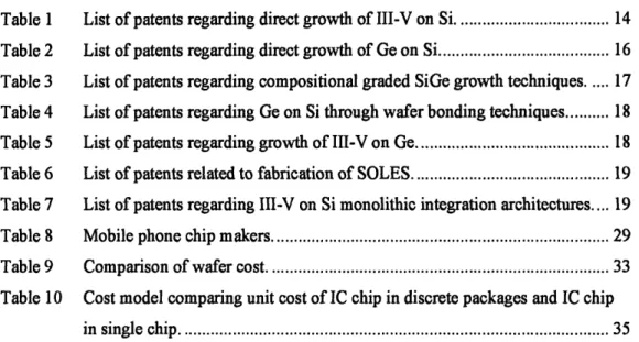
A silicon on lattice-engineered substrate (SOLES) consists of a compositionally graded Sil,-xGex buffer buried underneath a silicon-on-insulator (SOI) structure, on top of a silicon substrate. ['l A schematic drawing of SOLES exposing both the silicon active layer and the III-V active layer is shown in Figure 2. A SOLES substrate has a top layer of silicon, which allows the fabrication of Si-based devices. Through etching, the Sil-xGex graded buffers with Ge cap layer can be uncovered. The Sil-xGex graded buffers have been proven to be a viable platform for fabrication of GaAs-based devices since Ge and GaAs are closely lattice-matched. [2-101 In such a way, Si-based devices and GaAs-based
devices can be integrated on the same platform.
Figure 2 Schematic drawing of SOLES. (Not drawn to scale)
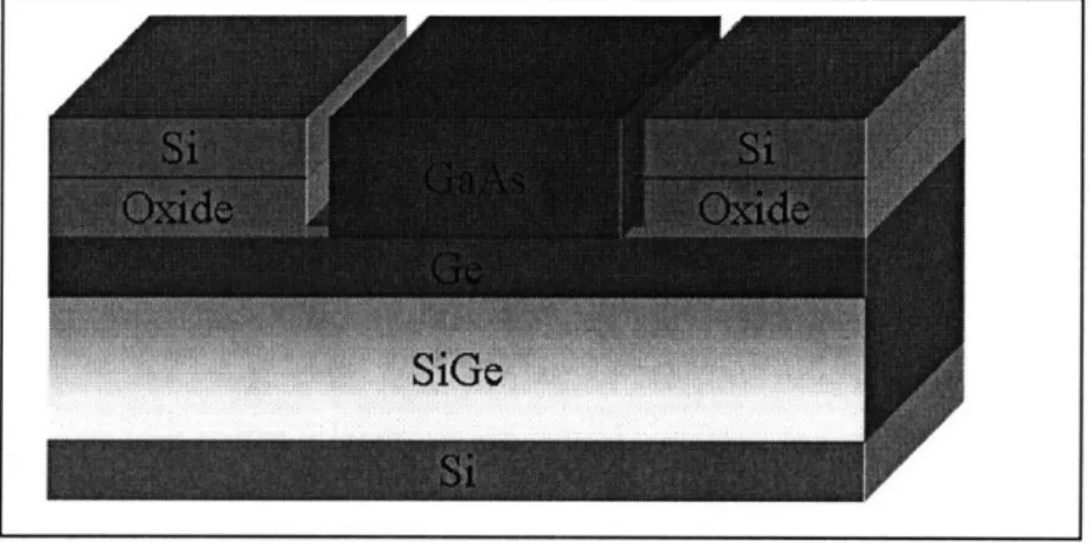
Figure 3 shows the fabrication steps of SOLES. Compositionally graded Sil-xGex buffers were grown from pure Si to a Ge-rich alloy by ultra-high-vacuum chemical vapor deposition (UHVCVD), followed by deposition of SiO2 by low pressure chemical vapor
deposition (LPCVD) and chemical mechanical polishing (CMP) of SiO2 surface. This
handle wafer is then wafer bonded to a Si donor wafer with a thermal oxide layer on top through SMARTCUT technique. Ell
SiO, planarized by CMP
LPCVD $102
Damaged
Si surface
LPCVD SiO2
LPCVD Si02
Bond
"
•interface
Figure 3 Fabrication steps of SOLES. 'I
Buried SiO
2i
|
li·r~rtMc*l·n~·u~rr~·*·i,,i·cnlr,3·.1·r
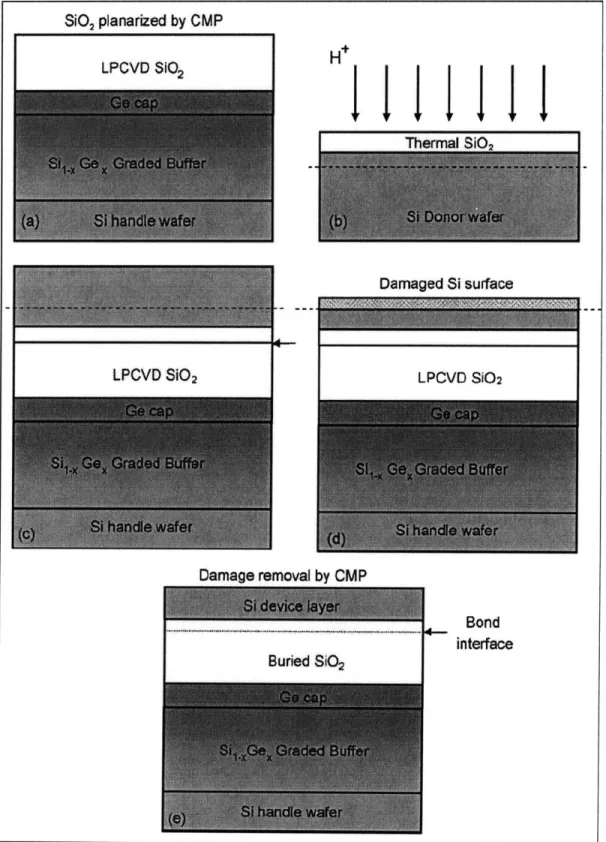
Monolithic integration of Si CMOS with AlGalnP light-emitting diode (LED) using SOLES platform has been demonstrated. ["I Figure 4 shows how the III-V-based LED can be integrated with the Si-based transistors in close proximity.
CMOs
LED
Transistor
Figure 4 Schematic of monolithic integration achieved using the SOLES substrate. II)
As noted in SOLES, III-V devices are grown on the SiGe compositional graded buffer. High quality GaAs epitaxy with low dislocation density (-106/cm2) has been
fabricated on SiGe compositional graded buffer. [12] Researchers have progressively
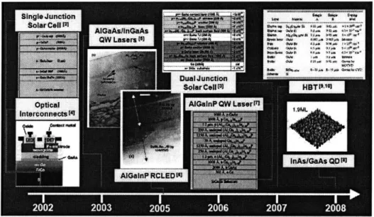
demonstrated various III-V-based devices on the SiGe/Si platform since 2000. Figure 5
shows the milestone for III-V devices on SiGe/Si platform. [2-10] Single junction and dual junction InGaP/GaAs solar cells have been fabricated on the platform and have total area efficiency (TI) of -18%. Effort has been put in to improve solar cell efficiency, as well as
other parameters that indicate the performance of solar cells, such as open circuit voltage (Voj), maximum short circuit current density (J8,) and fill factor (FF). [2,3] Many optical
devices, such as lasers, LED, and optical interconnects, have been demonstrated on the SiGe/Si platform. However, the photoluminescence response and electroluminescence response, in general, are less ideal as compared to optical devices rooting on III-V substrate. In some cases, the total thickness of device layers is too large to avoid thermal cracking. Rooms remain for these optical devices to be further improved. 14-8] As for the monolithic integration of III-V electronics devices with Si CMOS, high gain HBT based
on A1GaAs/GaAs and InGaP/GaAs hetero-system have been reported. The fabrication of HEMT and MESFET with less complicated structures is pretty optimistic, and they should be able to be demonstrated in near future. [9, 10]
Figure 5 Milestone for III-V devices on SiGe/Si platform. 12-101
In conclusion, the demonstrated integration of III-V LED with Si CMOS can be applied to III-V based electronic devices. III-V HBT and HEMT can be integrated with Si CMOS in the same way.
Competing Technologies
Study of patent literature is important to understand the competition of monolithic integration platform. Broadly speaking, the approaches for monolithic integration of III-V on Si fall into two categories, (i) direct growth of III-III-V on Si, and (ii) growth of III-III-V on Si using Ge intermediate layer.
Quite a number of patents regarding direct growth of III-V on Si have been filed as shown in Table 1.
6,563,143 13 May STMicroelectron CMOS circuit of GaAs/Ge on Si substrate 2003 ics, Inc.
5,221,637 22 Jun Interuniversitair
1993 Micro
Elektronica Centrum vzw 5,281,551 25 Jan Korea Institute
1994 of Science and Technology 5,108,947 28 Apr AGFA-Gevaert 1992 N. V. 4,900,372 13 Feb Kopin 1990 Corporation 4,840,921 20 Jun NEC 1989 Corporation 4,699,688 13 Oct GTE 1987 Laboratories Incorporated
Mesa release and deposition (MRD) method for stress relief in heteroepitaxially grown GaAs on Si
Method for delta-doping in GaAs epitaxial layer grown on Si substrate by metal organic chemical vapor deposition
Integration of GaAs on Si substrates p/s: Deliberately introduce microcracks in GaAs layer
III-V on Si heterostructure using a thermal strain layer
Process for the growth of III-V group compound semiconductor crystal on a Si substrate
Growing of
III-V
epitaxy on Si is challenging due to the lattice mismatch and
thermal mismatch as depicted in Figure 6. These revealed growth techniques fail to
produce epitaxy of low dislocation density. In the attempt to lower the dislocation
density, an unreasonably thick buffer layer is used, which deteriorates the thermal
mismatch problem. Introduction of microcracks does help to mitigate the problem of
thermal mismatch; however, it does not reduce the misfit dislocations. Thus, patents in
the first category do not pose any threat to the commercialization of SOLES.
Thermal Expansion Coefficient vs. Lattice
Constant for Semiconductors
9.000
8.000 + GaSb
7.000 * GaAs
6.000 .GGe
* InSb
5.000 + AIAs 4 InP * AISb
GaP hInAs
S4000
3.000
E
S1.000oo (Data source: www.matweb.com)
0.000
5,200 5 400 5.600 5.800 6.000 6.200 6.400 6.600 Lattice Constant (A)
Figure 6 Thermal expansion coefficient vs. lattice constant for semiconductors.
Since the direct growth of
III-V
on Si has not yielded any positive outcome, the
alternative of growing
III-V
on Si with an intermediate layer starts to attract attention.
SOLES technique belongs to the second category, growing of
III-V on Si using a Ge
intermediate layer. Ge intermediate layer is an appealing choice for two obvious reasons.
Firstly, Ge can be deposited on Si through the growth of compositional graded SiGe
buffer or wafer bonding of SOI with GOI (germanium-on-insulator) or SGOI
(silicon-germanium-on-insulator). Secondly, Ge is lattice-matched with GaAs which allows the
deposition of various
III-V
materials. To systematically study the competition, the second
category shall be further subdivided into two parts, the growth of Ge on Si and the
growth of
III-V
on Ge.
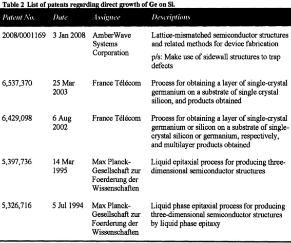
There are several patents showing how Ge can be directly grown on Si as listed in Table 2.
Table 2 List of stents re rai alrect th of Ge on Si.
3 Jan 2008 AmberWave Systems Corporation 25 Mar 2003 6,429,098 6 Aug 2002 France Telecom France Td1lcom
5,397,736 14 Mar Max Planck-1995 Gesellschaft zur
Foerderung der Wissenschaften 5,326,716 5 Jul 1994 Max
Planck-Gesellschaft zur Foerderung der Wissenschaften
Lattice-mismatched semiconductor structures and related methods for device fabrication p/s: Make use of sidewall structures to trap
defects
Process for obtaining a layer of single-crystal germanium on a substrate of single crystal silicon, and products obtained
Process for obtaining a layer of single-crystal germanium or silicon on a substrate of single-crystal silicon or germanium, respectively, and multilayer products obtained
Liquid epitaxial process for producing three-dimensional semiconductor structures
Liquid phase epitaxial process for producing three-dimensional semiconductor structures by liquid phase epitaxy
Direct growth of Ge epitaxy on Si is hampered by the 3-D islanding nature of this hetero-system. Beyond the critical thickness, Ge epitaxy evolves into 3-D islands to relieve the stress built up. As these islands coalesce, defects are created. Techniques listed in Table 2, in general, leads to Ge epitaxy of high dislocation density. The idea of using sidewall structures to trap defects is effective to reduce dislocation density, but the alignment issue during processing is challenging. Therefore, growth of Ge on Si is easier to be done by using compositional graded SiGe buffer.
2008/0001169
6,537,370
Massachusetts Institute of Technology and AmberWave Systems Corporation have fully staked their claims in the patent space of compositional graded SiGe techniques. Related patents are listed in Table 3.
Table 3 List of atents r rain com sitional raded SiGe owth techni ues.
7,368,308 6 May 2008 7,041,170 9 May 2006 6,927,147 9 Aug 2005 6,921,914 26 Jul 2005 6,876,010 5 Apr 2005 6,864,115 6,039,803 8 Mar 2005 AmberWave Systems Corporation AmberWave Systems Corporation Massachusetts Institute of Technology Massachusetts Institute of Technology Massachusetts Institute of Technology AmberWave Systems Corporation 21 Mar Massachusetts 2000 Institute of Technology
Methods of fabricating semiconductor heterostructures
Method of producing high quality relaxed SiGe layers
Coplanar integration of lattice-mismatched semiconductor with silicon via wafer bonding virtual substrates
Process for producing semiconductor article using graded epitaxial growth
Controlling threading dislocation densities in Ge on Si using graded GeSi layers and planarization
Low threading dislocation density relaxed mismatched epilayers without high temperature growth
Utilization of miscut substrates to improve relaxed graded SiGe and Ge layers on Si
Other than using a SiGe graded buffer to grow Ge on Si, Ge can be integrated with Si by wafer bonding an SOI wafer with an SGOI or GOI. Relevant patents are listed in Table 4.
''' ' '~' ' ' I
7,315,065 1 Jan 2008 International Method for fabricating SiGe-on-insulator Business (SGOI) and Ge-on-insulator (GOI) substrates Machines Corporation 26 Jun International 2007 Business Machines Corporation 20 Jul 2004 Advanced Micro Devices, Inc. 13 Jan AmberWave 2004 Systems Corporation
Method of creating defect free high Ge content (>25%) SiGe-on-insulator (SGOI) substrates using wafer bonding techniques
Semiconductor-on-insulator (SOI) wafer having a Si/SiGe/Si active layer and method of fabrication using wafer bonding
Silicon wafer with embedded optoelectronic material for monolithic OEIC
It is shown that growth of Ge on Si is feasible using a compositional graded SiGe layer or an oxide layer. For Ge to be a viable choice of intermediate layer for monolithic integration of Si and III-V, Ge-GaAs heterogeneous interface is the next issue. A few patents illustrate that GaAs can be grown on top of Ge, as listed in Table 5. These patents have very narrow claims and they are not critical for growing III-V epitaxy of good quality.
5,308,444 3 May AT&T Bell Method of making semiconductor 1994 Laboratories heterostructures of GaAs on Ge 4,835,116 30 May Kopin Annealing method for III-V deposition
1989 Corporation
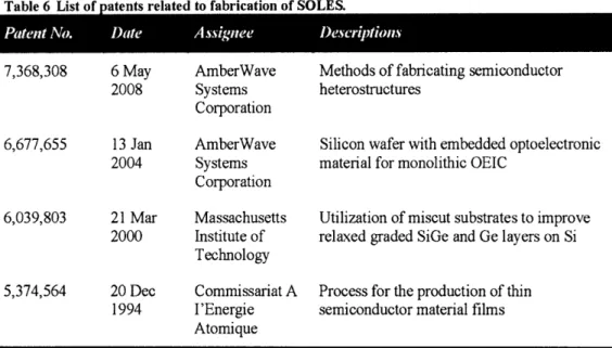
Fabrication of SOLES substrate has made use of several patented techniques, as listed in Table 6. Therefore, in the process of commercialization, SOLES manufacturers shall pay royalty to these assignees.
7,235,812
6,765,227
Table 6 List of atents related to fabrication of SOLES.
RietN. Die Asge ecD~in
7,368,308 6 May AmberWave 2008 Systems Corporation 6,677,655 13 Jan AmberWave 2004 Systems Corporation 6,039,803 5,374,564 21 Mar Massachusetts 2000 Institute of Technology 20 Dec Commissariat A 1994 I'Energie Atomique
Methods of fabricating semiconductor
heterostructures
Silicon wafer with embedded optoelectronic material for monolithic OEIC
Utilization of miscut substrates to improve relaxed graded SiGe and Ge layers on Si
Process for the production of thin semiconductor material films
Competing techniques in forming device-quality heterogeneous interface between III-V and Si have been addressed in the above discussion. Subsequently, various competing monolithic integration solutions are discussed. There are several configurations of integrating III-V on Si substrate. Table 7 shows two patented III-V on Si monolithic integration solutions. Besides, there is another monolithic integration configuration proposed by T. Akatsua et al. which has yet to be patented. [13]
7,259,084 21 Aug 2007 6,737,670 18 May
2004
National Chiao- Growth of GaAs epitaxial layers on Si Tung University substrate by using a novel GeSi buffer layer Massachusetts
Institute of Technology
Semiconductor substrate structure
For SOLES to be commercialized, it has to compete with the three abovementioned monolithic integration solutions. Figure 7 shows the comparison of
these four different techniques. The concerns of commercializing a monolithic platform are: (i) ease of processing, (ii) economies of scale, and (iii) contamination issues.
I
Oxide
I
US patent no.: 7,259,084
US patent no.: 6,737,670
nvide I
Si
T. Akatsua et al.
Figure 7 Comparison of four monolithic integration solutions (not drawn to scale).
The height difference between Si active layer and GaAs active layer gives rise to processing difficulties both in front-end and back-end. The occurrence of tiny III-V extrusions throughout the wafer is a nuisance in wafer processing. It degrades the resolution of lithography because depth-of-focus has to be maintained high enough for the uneven surface. The SOLES is the only technique among the four which can integrate both active layers of Si and GaAs with negligible height difference.
(3)
SOLES
The main motivation of monolithic integration is to reproduce the large
economies of scale of Si platform. Integration techniques that fail to preserve the large
economies of scale would lose their competencies. Taking into account of this issue, the
technique proposed by T. Akatsua et al. that involves wafer bonding of Ge-on-insulator
and Si-on-insulator is inferior, because it is limited by the small size Ge wafer. However,
the transferable metamorphic Ge epitaxy has resolved this issue. Ge epitaxy can be
transferred from Si platform to form GOI of large wafer size.
Having Ge-terminated surface could be one of the hurdles for the industry to
adopt these monolithic integration solutions. Ge-terminated surface can be easily
oxidized to GeO
2 which is very volatile, causing contamination problems. A SOLES hasa Si-terminated surface, which distinguishes itself from the other Ge-terminated
platforms.
Among these monolithic integration solutions, SOLES turns out to be best choice
in terms of ease of processing, high production volume and low contamination.
Potential Applications
Potential applications of SOLES are a subset of all III-V compound
semiconductor applications. III-V compound semiconductors are used for wireless
communication, optical fiber communication, lighting and display, solar cells, optical
storage, instrumentation, optical interconnects and so on. From the list of applications,
one has to identify those applications for which integration of III-V-based devices and
Si-based devices is important.
A few areas
(i)
(ii) (iii) (iv)
of applications are shortlisted, namely,
wireless communication,
optical fiber communication,
optical storage and
optical interconnects.
In this project, only integration of electronics devices would be discussed. Optical
fiber communication, optical storage and optical interconnects, which are the photonics
applications of SOLES, would be addressed in another project. Thus, wireless
applications become the sole focus.
III-V compound semiconductors are suitable for wireless applications because
they have:
(i)
high cut off frequency, fT (the frequency at which the short circuit current
gain becomes unity),
(ii)
high maximum frequency of oscillation, fm (the frequency at which the
unilateral power gain becomes unity),
(iii)
low minimum noise figure, NFwnn,
(iv)
wide range of output power
Poutand high output power density
PDoutat high
frequency regime.
For wireless applications, RF switches, transceivers and power amplifiers are
usually made out of compound semiconductor materials. However, these III-V
components do not work independently. They need to be supported by Si-based CMOS
circuitry for the purpose of internal signal processing.
The wireless communication industry is working hard on single chip solution. The
prospective advantage of single chip solution is not only the reduction in size, but also the
reduction in cost. Currently, the single chip solution is achieved by replacing the
III-V-based components with SiGe-III-V-based components. However, such single chip solution
solves only the short term problem. SiGe devices achieve high frequency performance
through scaling down and such small transistor can only drive small current. Excessive
scaling would end up with low power transistors which are completely useless.
Furthermore, SiGe HBTs are relatively noisy as compared to III-V HBTs. SiGe will lose
losing its market as wireless technology develops towards high power high frequency
applications. The SiGe-based RF components have approached their limits and could
hardly fulfill the stringent high frequency requirements. It is believed that III-V devices
would be the ultimate choice for these high frequency high power applications. The need
of single chip solution for III-V based RF components thus arises. The SOLES is the
answer to this single chip solution. Without a monolithic platform, IC chipsets for
wireless applications using III-V based RF components are in discrete packages. Given a
monolithic platform like SOLES, III-V based RF components can be integrated with
Si-based digital baseband and the single chip solution becomes possible.
In the context of wireless, it can be subdivided into the following applications:
* Mobile phone communication
* Wireless network
o Wireless local area network (WLAN)
o Wireless metropolitan area network (WMAN)
o Wireless wide area network (WWAN)
* Bluetooth*
* Automotive radar
* Military applications
* Space applications
From the list of wireless applications, SOLES should focus on consumer
electronic products rather than high-end applications like automotive radar, military
applications and space applications. For these high-end applications, the production
volume is small and cost of chips is not important. Since commercialization of SOLES is
still at the beginning stage, more attention should be paid to applications that require
high-volume and low-cost. However, the potential of SOLES in these high-end markets
should not be underestimated. The SOLES offers performance advantages by simply
integrating all devices in a closer proximity, which allows the system to work at higher
power and faster speed. Thus, the use of SOLES in high-end applications is possible in
future.
Commercialization of SOLES should emphasize on those consumer electronic
products with very high demand and large market. According to the report of iSuppli
Corp., the sales of wireless chip grew by 7.6% to
$29.5
billion in 2007 given that growth
rate of the overall chip market was only 3.3%. This is an indication of the prosperity of
wireless market. Commercialization of SOLES should focus on IC chips in consumer
electronic products, such as mobile phones, wireless network enabled devices,
Bluetooth® embedded products and GPS products, where cost and performance are
equally important. Among the abovementioned applications, mobile phone and wireless
network chips should be paid more attention to because they have the largest market
share and highest market growth rate. Approximately 986 million units of handsets were
sold in year 2006 and the number will continue soaring, as revealed by Plunkett Research,
Ltd. Statistics from Research and Markets Ltd has quantified the shipments of WiFi
chipsets. 140 million units of WiFi chipsets have been shipped in year 2005 and the
number is forecasted to reach 430 million in year 2009.
The use of SOLES in mobile phone and wireless network will be discussed. To justify the need of SOLES in mobile phone IC chipsets, components in a mobile phone have to be understood. A typical mobile phone has four types of components, namely active components, passive components, structure components and functional components. Passive components refer to capacitors, inductors and resistors whereas structure components are the printed circuit boards (PCBs) and casing. Acoustic component, vibrating motor, display, battery and antenna are grouped under the functional components. The hardcore of a mobile phone lies on the active components, which include digital baseband, analog baseband, memory, transceiver, power amplifier and switches. Figure 8 shows a block diagram of a typical mobile phone. Front-end modules, switches and power amplifiers are usually made of III-V whereas the digital baseband and analog baseband are usually made of Si. Transceiver can be made of either Si or III-V. The Si technology, particularly SiGe HBT, has tried hard to win over III-V HBT in the game of power amplifier in mobile phone, but it failed. There are two possible reasons behind this. Firstly, SiGe HBT is too noisy to maintain the voice quality of mobile phone while working at frequency range of 400MHz to 1800MHz. Secondly, the power delivered by high frequency SiGe HBT is too small to meet the desirable working distance. The SOLES provides a platform for single-chip integration without compromising the performance of each device.
laniiD nm loAf baseband baoband
* aeba AO, DA) (•4
*--Pow" nmastmnt O8pIlay +--IKeyboad ,.. USEd, 1,0., 4·
+---)
Mlcrophone I- Vkcehandr@4 code. €I4
, r la 4 |OIAh4 WA)do(Source: III-Vs Review. Vol 19 - No 26 2 -March 2006)
Figure 8 Mobile phone block diagram.
Subsequently, the market of wireless network is studied. The wireless system
needs III-V to handle the high frequency high power applications and Si to handle the
logic processing. The current wireless solution stretches across a wide range of powers
and frequencies, as shown in Figure 9. The increasing importance of WiFi and WiMax
(Worldwide Interoperability for Microwave Access) shows that short-distance
optical-fiber-free data transfer is gaining its importance. According to the IEEE (Institute of
Electrical and Electronics Engineers, Inc) standard, WLAN 802.11 WiFi technologies
have several subgroups, 802.1 la/b/g/n. They differ in frequency (2.4GHz or 5GHz) and
maximum data transfer rate (11Mbps or 54Mbps). In Europe, HiperLAN2 standard set by
ESTI (European Telecommunications Standards Institute), which is similar to the IEEE's
802.1 la, is in use. The connectivity remains functional if it is within the range of the
wireless access point, which is not more than 300 feet (95 meter). WiFi is now embedded
in more and more electronic products, besides wireless routers, WiFi chips are found in
mobile phones, TV sets, game consoles, printers, and home stereos. Beyond WiFi,
WiMAX (WMAN 802.16 IEEE standard or HiperWAN ESTI standard) which works at
frequency range of 2 to 11 GHz is the emerging technology. It provides connectivity in a
larger geographic area than Wi-Fi. Various cities, including Tokyo, Amsterdam, Paris,
Philadelphia, have embarked on projects to create "Metro WiFi". The market is pushing
for an optical-fiber-free connectivity that has a working range long enough to serve the
whole city. Currently, single chip WiFi solution is available for certain applications.
Front-end modules and power amplifiers of single chip WiFi are made of SiGe devices.
Unlike the mobile phone, the role of III-V is taken over, possibly because WiFi has a
shorter working range that makes the RF requirements less stringent. Nevertheless,
SiGe-enabled single chip solution may not be useful as the technology moves towards higher
frequency higher power applications. Therefore, SOLES could be more useful for
WWAN applications.
Output Power (dBm) (Source: IEEE 802 Plenary, 2007)
3.3 3.8 4.7 4.9 5,.1 6.2 5.3 5.47 5.7
Frequency (GHz)
Figure 9 Range of powers and frequencies for wireless applications.
Supply Chain Analysis
The wireless IC supply chain for consumer electronics products, for instances,
mobile phones, WiFi devices, and WiMax devices is discussed in this chapter. As
mentioned in the previous chapter, wireless IC chipsets have several important active
components, such as baseband, transceiver, power amplifier, and memory. Each of them
is supplied by different vendors.
The mobile phone IC chip makers are tabulated in Table 8. Baseband chip are the
priciest items in mobile phone IC chipsets as it carries the highest technical content.
Texas Instruments (TI), the main baseband supplier for Nokia and Sony Ericsson, has
been the leader in baseband chips for years. Recently, its leading position has been taken
over by Qualcomm as reported by iSuppli Corp in May 2008. In order to reduce the
number of IC packages in mobile phones, transceiver chip has been integrated with
baseband chip, on the Si platform. Integration of transceiver with baseband has put
Qualcomm in an advantageous position due to its monopoly power in CDMA transceiver.
Memory chip, which is the second most expensive item in mobile phone, is mainly
supplied by Spansion, Samsung and Toshiba. Among the big three, Spansion has the
largest market share as it nearly monopolizes memory chips supply of low-end mobile
phones. RFMD and Skyworks are the major power amplifier suppliers. A power
amplifier is perhaps the most important component of a mobile phone as it determines the
call quality, signal receiving ability, battery life and other essential aspects. Fabrication of
the current GaAs-based power amplifiers is very cost-effective, leading to very high
gross profit margin. Therefore, Si-based power amplifiers can hardly defeat GaAs power
amplifiers in terms of cost and performance.
Table 8 Mobile phone chip makers.
B asban Y~eorrPowrA mQ-tr Trnscive
Spansion Samsung Toshiba STMicroelectronics Intel Elpida Winbond Etron ESMT RFMD Skyworks Renesas Freescale NXP Avago Triquint Anadigics Qualcomm STMicroelectronics Infineon TI Renesas RFMD Skyworks
The competition among WiFi IC suppliers is more intense. WiFi IC chipsets embedded in different electronic products have to meet different specifications. Hence, WiFi IC suppliers have to come out with completely distinct system designs to cater to different needs. Broadcom, Intel, Atheros and Marvell are leaders of WiFi chips, who have successfully introduced single chip WiFi to the market. Their market share is shown in Figure 10. For non-single-chip WiFi solution, power amplifiers, memory and other chips are present in the system, like the case of mobile phone.
Figure 10 Worldwide WiFi chip market share in 2006. Qualcomm TI NXP Freescale Infineon Toshiba MTK ADI Skyworks NEC
(Data source: IDC, Broadcom)
Other
Ai•-* I
Conexant
theros, 16%
A WiMax system consists of two parts, a WiMax tower and a WiMax receiver.
WiMax wireless network is still in the introductory phase where the companies involved
are mainly new start-ups or young enterprises. Consider IC for a WiMax system,
baseband chipset and RF chipset are the most essential building blocks. Intel, Sequans,
Picochip, Wavesat Wireless and Fujitsu Microelectronics America (FMA) are the major
WiMax baseband chipset suppliers; whereas Sierra Monolithics, SiGe Semiconductor,
Analog Devices (ADI), RF Magic are the major WiMax RF chipset suppliers. These
chipmakers supply chips to WiMax manufacturers, such as Mitsumi, to set up the WiMax
tower or to incorporate chipset in a WiMax enabled device.
In a simplistic view, the supply chain of wireless IC can be represented by Figure
11. As noted, there are two scenarios, depend on whether the IC is built on pure Si
platform or two separated platform of Si and III-V. For wireless IC in mobile phone, the
supply chain follows Figure 1 (a). It involves two materials system, silicon and III-V.
Silicon and III-V wafers are processed into chips by different manufacturers. The
packaged chips, together with other passive components and structural components, are
assembled. For WiFi and WiMax, the choice of RF components, either III-V-based RF or
SiGe-based RF, determines the supply chain. For single chip WiFi and pure Si-based
WiFi/WiMax modules, the supply chain is as shown in Figure 1 l(b).
Figure 11 Supply Chain of Wireless IC. (a) Consmimei
SIC Waer
By introducing SOLES into the supply chain, the chip manufacturers would
fabricate Si-based devices and V-based devices on SOLES instead of Si wafers or
III-V wafers. With a monolithic SOLES platform, every individual chip contains both Si and
III-V devices. A modified supply chain is shown in Figure 12.
Figure 12 Modified Supply Chain.
SOLES substrates will affect the current wafer supply. Fabrication of SOLES
requires Si wafers, which are supplied by Shin-Etsu, Sumco, Siltronic and MEMC. The
introduction of SOLES IC chips eliminates the use of III-V wafers. III-V wafer suppliers
like Wafer Technology, RFMD, AXT, InPACT, Nikko Materials USA and Sumitomo
Electric will be affected.
Consumers Second Level Packaging SOLES Chip SOLES Wafer Other Components
Cost Analysis
In this chapter, a cost analysis will be carried out for SOLES single chip solution
and wireless IC chipset in discrete packages.
Switching from discrete packages to SOLES single chip solution can reduce the
production cost significantly by eliminating the need of packaging individual III-V and Si
chips. Packaging cost is a big part of the overall cost, ranging from 20% to 80%.
Moreover, SOLES has avoided the use of expensive III-V wafers. Instead, it makes use
of two cheap silicon wafers. Combining two or more chips into one, a reduction in total
chip size is possible by reducing the number of I/O pin counts. The use of bigger wafers
and the reduction in chip size yield more chips per wafer, leading to cost reduction. The
device fabrication cost could be lowered further by reducing the number of masks.
However, the fabrication cost of a SOLES substrate has to be considered. Cost of wafer
bonding and cost of growing SiGe graded buffer have to be accounted for. Since the
chips on SOLES substrate have high IC complexity, lower yield is expected.
To quantify the abovementioned qualitative cost advantages and disadvantages of
SOLES, a cost model has been developed. Consider an IC chipset in a mobile phone or in
a WLAN/WMAN/WWAN device, the unit costs of both cases are compared. To simplify
the discussion, it is assumed that the discrete package IC chipset consists of one Si chip
and one GaAs chip, and using a SOLES substrate, the two chips are integrated as one.
There are three important cost components, the wafer fabrication cost, packaging cost and
testing cost. The cost model approximates that each of these components is one third of
the total cost. The fabrication cost per wafer is estimated by considering the average cost
per mask. The number of masks can vary depending on the complexity of the system.
The cost per chip is obtained by dividing the cost per wafer by the number of chips in a
wafer. Therefore, the cost of an IC chip is closely related the chip size.
There are a few important factors that determine if switching to SOLES platform
is beneficial. These factors are percentage of GaAs and Si, area of chip, number of masks,
and yield.
Comparing the wafer cost per unit area, GaAs wafers are expensive whereas Si
wafers are very cheap. SOLES wafers are 5 times more expensive than Si wafers but 40%
cheaper than GaAs wafers as shown in Table 9. Consider a system with high GaAs
percentage, using SOLES wafers is likely to result in cost saving, but it may not happen
for the case of low GaAs percentage. As the working frequencies are stretched to a higher
range, SiGe HBTs are very likely to be replaced by GaAs HBTs or HEMTs, resulting in
system of high GaAs percentage. However, the trend of consumer electronic market is to
make the products multi-functional. As other functions such as camera, radio, Bluetooth
and GPS are integrated into a mobile phone, the microprocessor which is usually made of
Si becomes more complex. It would possibly increase the percentage of Si in the system.
Thus, percentage of GaAs and Si is strongly dependent on performance specifications
and extra functions integrated in wireless products.
6" GaAs wafer
$200.00
$11.32
12" SOLES wafer
$480.00
$6.79
Chip area is another important factor to be considered. The comparative cost of
SOLES IC chip is strongly related to the area reduction that could be achieved while
switching from discrete packages to single chip solution. This is a circuit design issue.
Usually, a chip area reduction of 5-30% is possible for integrating two chips into one. A
single chip solution with larger chip area reduction will result in higher cost saving.
The number of masks is one of the key cost indicators. Si CMOS technology
usually requires 30-40 masks whereas the GaAs HBT technology needs 20-30 masks.
Masking levels of a single chip SOLES IC are anticipated to be lower, around 40-55
masks. The more the reduction of masks, more cost will be saved.
Process optimization is also important in determining the cost of an IC chipset.
The throughput yield for a high complexity IC chip is usually lower. Yield degrades
when switching to SOLES single chip solution. Thus, cost is increased.
A set of variables is input into the cost model, as shown in Table 10. From the
cost model, the cost of a SOLES IC chip is not much different from the cost of a
conventional IC chipsets in discrete packages. The 0.06% difference seems to be
insignificant. However, it does not imply that SOLES could not penetrate into the market.
The single chip SOLES poses an advantage in PCB assembly. Since the number of
packages has been reduced, the cost of alignment can be brought down significantly. This
cost saving is enjoyed by customers but it is not captured in this cost model.
GaAs chip Chip area= Wafer size (4", 6", 8")= Feature size(180, 130, 90nm)= Wafer area= No. of chip/wafer= Wafer cost= No. of masks= Fabrication cost/mask= Fabrication cost= Packaging cost= Testing cost= Yield= Total cost/wafer= Unit cost= Si chip Chip area= Wafer size (8",12",18")= Feature size(65, 45, 32nm)= Wafer area= No. of chip/wafer= Wafer cost= No. of masks= Fabrication cost/mask= Fabrication cost= Packaging cost= Testing cost= Yield= Total cost/wafer= Unit cost= 35 6 180 17671.46 504 200.00 25 45.00 1125.00 1125.00 1125.00 0.85 3575.00 8.35 45 12 65 70685.83 1570 90.00 36 90.00 3240.00 3240.00 3240.00 0.95 9810.00 6.58
GaAs chip + Si chip
Total unit cost=
mm2 inch nm mm2 units $ units $S $ $ $ $S $ mm2 inch nm mm2 units $ units $ $ $ $ SOLES chip Area reduction= Chip area= Wafer size (8",12", 18")= Wafer area= No. of chip/wafer= Pre-wafer bonding cost= Wafer bonding cost= Wafer cost= No. of masks= Fabrication cost/mask= Fabrication cost= Packaging cost= Testing cost= Yield degradation= Yield= Total cost/wafer= Unit cost-= Conclusion
(Discrete packages) Cost=
(SOLES single chip) Cost =
%Cost saving= 14.92 S 0.20 64 12 70685.83 1104 150.00 150.00 180.00 54 75.00 4050.00 4050.00 4050.00 0.05 0.77 12630.00 mm2 inch mm2 units $ $ $ units $ $ $ $ $ 14.91 $ 14.92 14.91 0.06%
Business Strategy
There are two common ways to start-up a new technology-based company. One
can either sell the license to incumbent manufacturers or set up a plant to manufacture
products. The two possibilities will be discussed respectively.
Considering the first scenario, licensing of SOLES technique to the existing
manufacturers is not really feasible. Neither the Si-based device manufacturers nor the
III-V-based device manufacturers would buy the license. Their research team will look
for alternatives to get around the SOLES technique.
The second scenario is to set up a plant to produce Si-based devices and III-V
based devices on SOLES platform. This involves very high investment in equipments.
Furthermore, fabrication techniques of Si and III-V devices are intellectual property of
existing chip makers. Thus, it is not advisable to invest in a production line.
In view of the above issues with licensing the technology and setting up
production line for SOLES chips, a relatively new business concept, the virtual vertical
integration model is introduced. It is a fabless company that holds the license of
technology. Through establishing partnership with one or more companies with required
production capacities, it fills up the gap between segments of supply chain.
To fit the virtual vertical integration model into the context of SOLES, the new
start-up company shall approach Si-based device manufacturers and III-V-based device
manufacturers to seek for partnership. With their fabrication facilities, the company can
produce SOLES wafers, monolithically integrate all devices on SOLES wafers, package
the SOLES chips and sell them to customers.
SOLES chips have the potential to gain a substantial market share, by claiming
that they could reduce the assembly cost significantly. Such cost advantage is very
attractive from the perspective of a customer. The development of WiFi multi-packages
IC chipsets into the current single-chip WiFi IC is a piece of concrete evidence showing
that replacing a multi-package chipset with single chip IC solution is cost-effective and
feasible.
Conclusions
III-V electronic devices, the HBTs have been demonstrated on SiGe/Si platform.
The device fabrication techniques should be able to apply to SOLES platform without
much technical barriers. Given the hypothetical scenario that III-V HBTs or HEMTs
could be integrated with Si CMOS on SOLES platform, the commercialization potential
of SOLES substrate is studied.
There exists opportunities for SOLES in the wireless market, especially in the
mobile phone market and in the wireless network market. SOLES chips enable the
monolithic integration of III-V devices and Si devices which is revolutionary for wireless
IC chipsets.
The technical competition in providing monolithic integration solutions and the
market competition among players in the supply chain are analysed. In comparison with
other monolithic platforms, the SOLES monolithic platform appears to be the best
candidate as of now. On the other hand, players in the supply chain are interacting very
competitively. Their technology power determines their market share and rankings.
The cost effectiveness of SOLES IC chip is investigated by developing a simple
cost model. The cost model shows that SOLES may not be able to reduce cost of chips to
a large extent. However, its potential to reduce the assembly cost would be appreciated
by customers, such as mobile phone manufacturers and wireless network device
manufacturers. Therefore, the possibility for SOLES to grab a pie in the market is
optimistic.
Establishing partnerships with the current chip makers is important in the
commercialization of SOLES. As justified previously, it would be more feasible for the
new start-up to partner with existing manufacturers and start producing SOLES chips
using their production facilities.
In short, there are two immediate issues need to be resolved for SOLES to be
commercialized:
(1)
More engineering research needs to be carried out to optimize the
performance of devices on SOLES platform, and to demonstrate a good
single-chip SOLES wireless IC design.
(2)
Joint effort from partners in the early stage of commercialization is
incredibly important. Partnerships shall be established as soon as possible
so that the customers could be identified and design effort could be more
directional.
Having addressed the two issues mentioned above, the SOLES technique is ready
for near term commercialization.
References
[I] C. L. Dohrman, K. Chilukuri, D. M. Isaacson, M. L. Lee, E. A. Fitzgerald,
Fabrication of silicon on lattice-engineered substrate (SOLES) as a platform for monolithic integration of CMOS and optoelectronic devices, Materials Science
and Engineering B 135 (2006) 235-237.
[2] S.A. Ringel, J.A. Carlin, C.L. Andre, M.K. Hudait, M. Gonzalez, D.M. Wiltz, E.B. Clark, P. Jenkins, D. Scheiman, A.Allerman, E.A. Fitzgerald, C.W. Leitz,
Single-junction InGaP/GaAs Solar Cells Grown on Si Substrates with SiGe Buffer Layers, Prog. Photovolt: Res. Appl. 10 (2002) 417-426.
[31 M.R. Lueck, C.L.Andre, A.J. Pitera, M.L. Lee, E.A. Fitzgerald, S.A. Ringel, Dual
junction GalnP/GaAs solar cells grown on metamorphic SiGe/Si substrates with high open circuit voltage, IEEE Elec. Dev. Lett. 27 (2006) 3.
[4] V.K. Yang, M.E. Groenert, G. Taraschi, C.W. Leitz, A.J. Pitera, M.T> Currie, Z. Cheng, E.A. Fitzgerald, Monolithic integration oflll-V optical interconnects on Si
using SiGe virtual substrates, J. Mater. Sci. Mater. Electron. 13 (2002) 377.
[5] M.E. Groenert, C.W. Leitz, A.J. Pitera, V. Yang, H. Lee, R.J. Ram, E.A.
Fitzgerald, Monolithic integration of room-temperature cw GaAs/AIGaAs lasers
on Si substrates via relaxed graded GeSi buffer layers, J. Appl. Phys. 93, No.1
(2003) 362-7.
[61 O.Kwon, J. Boeckl, M.L. Lee, A.J. Pitera, E.A. Fitzgerald, S.A. Ringel, Growth
and properties ofAlGaInP resonant cavity light emitting diodes on Ge/SiGe/Si substrates, J. Appl. Phys. 97 (2005) 034504.
[7] O.Kwon, J. Boeckl, M.L. Lee, A.J. Pitera, E.A. Fitzgerald, S.A. Ringel,
Monolithic integration ofAlGalnP laser diodes on SiGe/Si substrates by molecular beam epitaxy, J. Appl. Phys. 100, (2006) 013103.
I K.L. Lew, S.F. Yoon, W.K. Loke, H. Tanoto, C.L. Dohrman, D.M. Isaacson and E.A. Fitzgerald, High gain AlGaAs/GaAs heterojunction bipolar transistor
fabricated on SiGe/Si substrate, J. Vac. Sci. Technol. B, Vol. 25, 3 (2007).
[91 K.L. Lew, S.F. Yoon, H. Tanoto, K.P. Chen, C.L. Dohrman, D.M. Isaacson and E.A. Fitzgerald, InGaP/GaAs heterojunction bipolar transistor grown on Si
substrate with SiGe graded buffer layer, Electronics Letters, Vol. 44, 3 (2008).
['01 H. Tanoto, S.F. Yoon, C.Y. Ngo, W.K. Loke, C. Dohrman, E.A. Fitzgerald, B. Narayanan, Structural and optical properties of stacked self-assembled
InAs/InGaAs quantum dots on graded Sil.xGe/Si substrate, Appl. Phys. Lett. 92,
(2008)213115.
11 K. Chilukuri, M. J. Mori, C. L. Dohrman, E. A. Fitzgerald, Monolithic
CMOS-compatible AlGalnP visible LED arrays on silicon on lattice-engineered substrates (SOLES), Semicond. Sci. Technol. 22 (2007) 29-34.
[12] S.M. Ting, E.A. Fitzgerald, Metal-organic chemical vapor deposition ofsingle
domain GaAs on Ge/GexSi1_./Si and Ge substrates, J. Appl. Phys. 87 (2000) 2618.
[13] T. Akatsua, C. Deguetb et al., Germanium-on-insulator (GeOI) substrates--A
novel engineered substrate for future high performance devices, Materials
Appendix 1 Relevant Patents
(Sorted by decreasing patent number)
* SOLES fabrication related patents (important claims are included)
Metnoas of tabricating semiconductor heterostructures
Dislocation pile-ups in compositionally graded semiconductor layers are reduced or eliminated, thereby leading to increased semiconductor device yield and manufacturability. This is accomplished by introducing a semiconductor layer having a plurality of threading dislocations distributed substantially uniformly across its surface as a starting layer and/or at least one intermediate layer during growth and relaxation of the compositionally graded layer. The semiconductor layer may include a seed layer disposed proximal to the surface of the semiconductor layer and having the threading dislocations uniformly distributed therein.
Important claims:
1. A method of forming a relaxed graded semiconductor layer on a substrate, the method comprising the steps of: providing a semiconductor substrate; and epitaxially growing over the semiconductor substrate a relaxed graded layer comprising a first material and a second semiconductor material, with increasing content of the second semiconductor material at a grading rate exceeding about
25% per micrometer to a final composition having a content of the second
semiconductor material ranging from greater than 0% to 100% and a threading dislocation density not exceeding about 107/cm2.
2. The method of claim I wherein the relaxed graded layer has a dislocation pile-up density not exceeding about 20/cm.
3. The method of claim 1 wherein the relaxed graded layer has a dislocation pile-up density not exceeding about 1/cm.
4. The method of claim 1 wherein the relaxed graded layer has a dislocation pile-up density not exceeding about 0.01/cm.
5. The method of claim 1 wherein the grading rate is at least 30% of the second
semiconductor material per micrometer.
6. The method of claim 1 wherein the grading rate is at least 40% of the second semiconductor material per micrometer.
7. The method of claim 1 wherein the epitaxial growth occurs at a temperature ranging from about 600' C. to about 1200' C.
slug 2 a VaXMV1r -ussuxUs
1GU0If
RHU%-TC-UVIIIIISUIRLUaT (k11)
substrates
A method for fabricating germanium-on-insulator (GOI) substrate materials, the GOI substrate materials produced by the method and various structures that can include at least the GOI substrate materials of the present invention are provided. The GOI substrate material include at least a substrate, a buried insulator layer located atop the substrate, and a Ge-containing layer, preferably pure Ge, located atop the buried insulator layer. In the GOI substrate materials of the present invention, the Ge-containing layer may also be referred to as the GOI film. The GOI film is the layer of the inventive substrate material in which devices can be formed.
This invention provides a process for growing Ge epitaxial layers on Si substrate by using ultra-high vacuum chemical vapor deposition (UHVCVD), and subsequently growing a GaAs layer on Ge film of the surface of said Ge epitaxial layers by using metal organic chemical vapor deposition (MOCVD). The process comprises steps of, firstly, pre-cleaning a silicon wafer in a standard pre-cleaning procedure, dipping it with HF solution and prebaking to remove its native oxide layer. Then, growing a high Ge-composition epitaxial layer, such as Sio.iGeo.9in a thickness of 0.8 pm on said Si substrate by using
ultra-high vacuum chemical vapor deposition under certain conditions is demonstrated.
Thus, many dislocations are generated and located near the interface and in the low of
part of Siol.Geo.
9due to the large mismatch between this layer and Si substrate.
Furthermore, a subsequent 0.8 pm Sio.osGe0.
95 layer, and/or optionally a further 0.8 pmSio.02Geo.
98layer, are grown. They form strained interfaces of said layers can bend and
terminate the propagated upward dislocation very effectively. Therefore, a film of pure
Ge is grown on the surface of said epitaxial layers. Finally, a GaAs epitaxial layer is
grown on said Ge film by using MOCVD.
isetnuu or creaung
aerect iree
nign tie content (>z5/Yo) biUe-on-insulator (SGUI)substrates using wafer bonding techniques
A method for achieving a substantially defect free SGOI substrate which includes a SiGe
layer that has a high Ge content of greater than about
25
atomic % using a low
temperature wafer bonding technique is described. The wafer bonding process described
in the present application includes an initial prebonding annealing step that is capable of
forming a bonding interface comprising elements of Si, Ge and 0, i.e., interfacial SiGeO
layer, between a SiGe layer and a low temperature oxide layer. The present invention also
provides the SGOI substrate and structure that contains the same.
Iacutuou ui p ouuuwug ulgul quality reTrlaxeu 3ie Iayers