by Tymon Barwicz
B.Eng. Engineering Physics (2000) École polytechnique de Montréal
Submitted to the Department of Materials Science and Engineering in Partial Fulfillment of the Requirements for the Degree of
Doctor of Philosophy in Materials Science and Engineering at the
Massachusetts Institute of Technology September 2005
© 2005 Massachusetts Institute of Technology All rights reserved
Signature of Author... Department of Materials Science and Engineering August 1, 2005 Certified by ... Henry I. Smith Joseph F. and Nancy P. Keithley Professor of Electrical Engineering
Thesis Supervisor
Certified by ... Harry L. Tuller Professor of Ceramics and Electronic Materials
Thesis Supervisor
Accepted by ...
Gerbrand Ceder
R.P. Simmons Professor of Materials Science and Engineering Chair, Departmental Committee on Graduate Students
by Tymon Barwicz
Submitted to the Department of Materials Science and Engineering on August 1, 2005 in Partial Fulfillment of the
Requirements for the Degree of Doctor of Philosophy in Materials Science and Engineering
ABSTRACT
High-refractive-index-contrast microphotonic devices provide strong light confinement allowing for sharp waveguide bends and small dielectric optical resonators. They allow dense optical integration and unique applications to optical filters and sensors but present exceptional complications in design and fabrication. In this work, nanofabrication techniques are developed to address the two main challenges in fabrication of high-index-contrast microphotonic devices: sidewall roughness and dimensional accuracy.
The work focuses on fabrication of optical add-drop filters based on high-index-contrast microring-resonators. The fabrication is based on direct-write scanning-electron-beam lithography. A sidewall-roughness characterization and optimization scheme is developed as is the first three-dimensional analysis of scattering losses due to sidewall roughness. Writing strategy in scanning-electron-beam lithography and absolute and relative dimensional control are addressed.
The nanofabrication techniques developed allowed fabrication of the most advanced microring add-drop-filters reported in the literature. The sidewall-roughness standard-deviation was reduced to 1.6 nm. The field polarization and the waveguide cross-sections minimizing scattering losses are presented. An absolute dimensional control accuracy of 5 nm is demonstrated. Microring resonators with average ring-waveguide widths matched to 26 pm to a desired relative width-offset are reported.
Thesis Supervisor: Henry I. Smith
Title: Joseph F. and Nancy P. Keithley Professor of Electrical Engineering Thesis Supervisor: Harry L. Tuller
Chapter 1 Introduction... 19
PART I High-Index-Contrast Filters ... 23
Chapter 2 Background ... 25
2.1 Optical add-drop filters ... 25
2.2 Microring-Resonator Filters... 28
2.2.1 How They Work ... 28
2.2.2 Spectral Response of Microring Filters ... 30
2.2.3 Racetrack Resonators and Vernier Operation... 32
Chapter 3 Fabricated Add-Drop Filters ... 35
3.1 Introduction... 35
3.2 Structures Overview... 35
3.3 One-Layer Fabrication Process... 38
3.4 Fabricated Third-Order Filters... 40
3.4.1 First Third-Order Filters ... 40
3.4.2 First Frequency-Matched Filters... 45
3.4.3 Multistage Filters ... 49
3.4.4 Polarization-Independent Filters... 54
3.4.4.1 Integrated Polarization Diversity... 54
3.4.4.2 Two-Layer Fabrication Process ... 56
3.4.4.3 Fabricated Polarization-Independent Filters... 59
3.4.5 Summary ... 62
3.5 FSR-doubled Filters... 63
3.6 Conclusion ... 67
PART II Sidewall Roughness... 69
Chapter 4 Roughness Characterization... 71
4.1 Introduction... 71
4.2 Roughness Model... 73
4.3 Measuring Roughness: Methodology ... 74
4.3.1 Acquiring Micrographs... 74
4.3.2 Obtaining f ( z ) from the micrographs... 75
4.4.1 Evolution of LER during fabrication of HIC microphotonic devices... 78
4.4.2 Study of resist ... 80
4.4.3 Study of RIE ... 81
4.5 Discussion... 82
4.6 Conclusion ... 83
Chapter 5 Roughness Optimization ... 85
5.1 Introduction... 85
5.2 Liftoff Optimization... 86
5.3 Reactive-Ion Etching Optimization ... 90
5.4 Resulting Sidewall Roughness... 91
5.5 Chemical Polishing ... 93
5.6 Conclusion ... 94
Chapter 6 Roughness-Induced Optical Loss ... 97
6.1 Introduction... 97
6.2 Roughness Model... 99
6.3 Volume Current Method... 101
6.4 Three-Dimensional Analysis ... 102
6.4.1 Problem Decomposition... 102
6.4.2 Impact of Waveguide Height, Field Polarization, Vertical Field-Shape, and Roughness Statistics... 106
6.5 High Index-Contrast... 112
6.5.1 Rationale ... 112
6.5.2 Dyadic Green’s Functions in One-Layer Media... 115
6.5.2.1 Coordinate System... 115
6.5.2.2 Dyadic Green’s Functions in Layered Media ... 116
6.5.2.3 Leading-Order Solution ... 119
6.5.3 Scattering Losses ... 121
6.6 Numerical Results... 124
6.7 Discussion... 128
6.7.1 Trends ... 128
6.7.2 Quick Scattering-Loss Estimates. ... 134
6.7.3 Extension of the Roughness Model ... 136
6.7.4 Propagation Loss in Fabricated Filters ... 137
6.8 Conclusion ... 143
PART III Dimensional Accuracy ... 145
Chapter 7 Pattern Fidelity ... 147
7.1 Introduction... 147
7.2 SEBL Writing Strategy... 147
7.3 Conclusion ... 151
Chapter 8 Process Calibration: Absolute Dimensional Control... 153
8.1 Introduction... 153
8.2 Process Calibration ... 154
8.3 Resulting Dimensional Control... 156
8.4 Conclusion ... 157
Chapter 9 Frequency Matching: Relative Dimensional Control... 159
9.1 Introduction... 159
9.2 Frequency Matching Strategy... 160
9.3 Proximity Function ... 161
9.4 Fast Proximity Effects Computation... 166
9.5 Predicted Microring Shapes... 168
9.6 Comparison of Predicted and Measured Dimensions... 172
9.7 Experimental Results ... 174 9.8 Conclusion ... 179 Chapter 10 Conclusions... 181 10.1 Summary of Accomplishments... 181 10.2 Future Work... 182 Appendix A Raith 150 ... 185
A.1 General Operation... 185
A.1.1 Introduction... 185
A.1.2 Column-Related Problems ... 186
A.1.3 Stage-Related Problems ... 187
A.1.4 Bugs ... 189
Fig. 2.1 Schematic of a modern optical network...26
Fig. 2.2 Add-drop-filter functionality. ...27
Fig. 2.3 Spectral response of an add-drop filter ...28
Fig. 2.4 Schematic and spectral response of a microring-resonator add-drop filter...29
Fig. 2.5 Schematic and spectral response of a third-order microring resonator...31
Fig. 2.6 Schematic of a racetrack-resonator add-drop filter...33
Fig. 2.7 Illustration of the Vernier effect ...34
Fig. 3.1 Designed series-coupled third-order microring filters...37
Fig. 3.2 One-layer fabrication process overview ...38
Fig. 3.3 Cross-section of a smooth SiN waveguide ...39
Fig. 3.4 Electron micrograph of the first third-order microring filters ...41
Fig. 3.5 Measured and simulated response of the first third-order microring filters ...44
Fig. 3.6 Micrograph and spectral responses of frequency-matched filters. ...46
Fig. 3.7 Cascaded third-order filters used to enhance the in-band extinction...49
Fig. 3.8 Electron micrographs of fabricated multistage filters ...50
Fig. 3.9 Spectral responses of fabricated multistage filters ...52
Fig. 3.10 Measured and calculated spectral responses at drop-ports of successive stages of a three-stage filter. ...53
Fig. 3.11 Integrated polarization-diversity scheme...54
Fig. 3.12 Integrated polarization splitter and rotator...55
Fig. 3.13 Polarization-independent fiber-to-chip coupler ...56
Fig. 3.14 Novel multilayer fabrication process used for the polarization independent add-drop-filters...57
Fig. 3.15 Electron micrographs of waveguide cross-sections obtained using the fabrication process presented in Fig. 3.14 ...58
Fig. 3.16 Schematic and optical micrograph of the polarization-independent add-drop filter. ...60
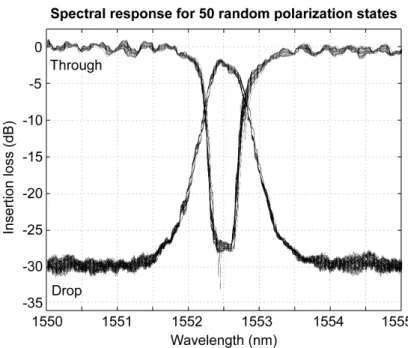
Fig. 3.17 Spectral response of a polarization independent add-drop filter for 50 random polarizations...61
Fig. 3.20 Spectral response of an FSR-doubled filter. ...66 Fig. 4.1 Schematic of a line with rough edges. Roughness is described by a
1D distribution with zero mean called f ( z ) . ...73 Fig. 4.2 Roughness spectral density estimates presenting the evolution of
line-edge roughness during fabrication of HIC microphotonic
devices...79 Fig. 5.1 Problems with liftoff of Cr...87 Fig. 5.2 Impact of resist profile on waveguide sidewall roughness ...89 Fig. 5.3 Top-view electron-micrographs of bus-waveguides from various
fabricated filters illustrating the sidewall roughness. ...92 Fig. 5.4 Side-view electron-micrograph of a ring-to-ring coupling gap
illustrating the sidewall roughness...93 Fig. 6.1 Schematic of a rough rectangular waveguide and spherical
coordinate system used ...99 Fig. 6.2 Decomposition of the radiation problem ...104 Fig. 6.3 Relation between two- and three-dimensional array-factors of a line
array. ...105 Fig. 6.4 Radiation efficiency of the x- and y-polarization for various
vertical-field-shapes and roughness statistics.. ...107 Fig. 6.5 Radiation efficiency of the z-polarization for various
shapes and roughness statistics, and schematic of the
vertical-field-profiles used...108 Fig. 6.6 Radiation profile of a point source with various polarizations and
forms of the power array-factors corresponding to various
vertical-field-shapes ...110 Fig. 6.7 Cross-section of the roughness power-array-factor for practical
roughness correlation lengths. ...112 Fig. 6.8 Actual and approximate dielectric distribution used for computation
of the radiation profile ...113 Fig. 6.9 Current sources in a one-layer medium and applicability of
free-space array factors...114 Fig. 6.10 Schematic of planar layered-media and rotated coordinated system
SiO2 (nclad=1.45) cladding...125
Fig. 6.13 Radiation efficiency of Si3N4 (ncore=2.00) waveguides embedded in a SiO2 (nclad=1.45) cladding...126
Fig. 6.14 Radiation efficiency of Si (ncore=3.50) waveguides embedded in a SiO2 (nclad=1.45) cladding...127
Fig. 6.15 Scattering losses in dB/cm normalized to the roughness variance in nm2 for SiON (ncore=1.50) waveguides embedded in a SiO2 (nclad=1.45) cladding ...129
Fig. 6.16 Scattering losses in dB/cm normalized to the roughness variance in nm2 for Si3N4 (ncore=2.00) waveguides embedded in a SiO2 (nclad=1.45) cladding ...130
Fig. 6.17 Scattering losses in dB/cm normalized to the roughness variance in nm2 for Si (ncore=3.50) waveguides embedded in a SiO2 (nclad=1.45) cladding...131
Fig. 6.18 Impact of roughness correlation length on scattering losses. ...134
Fig. 6.19 Illustration of deterministic roughness introduced by lithographic pixelization...142
Fig. 7.1 Electron micrographs demonstrating e-beam deflection errors introduced by the Raith 150...148
Fig. 7.2 Various e-beam vector-scanning strategies for microrings and observed problems in practice. ...149
Fig. 7.3 Micrograph of a lithographically perfect microring exposed in PMMA using the writing strategy presented in Fig. 7.2d...150
Fig. 8.1 Impact of e-beam proximity effects on absolute dimensional control...155
Fig. 9.1 Frequency matching strategies...160
Fig. 9.2 Empirical methods used to obtain the e-beam proximity function ...162
Fig. 9.3 Experimentally obtained e-beam proximity function ...165
Fig. 9.4 Resist clearing-dose contours in first frequency-matched filters for various exposure doses ...169
Fig. 9.5 Resist clearing-dose contours in multistage filters for various SEBL exposure doses. ...170
frequency-matched filters ...173 Fig. 9.8 Frequency mismatch observed in experiment at various
dose-compensations for first-frequency-matched filters and multistage
filters ...175 Fig. 9.9 Drift of the absolute resonant frequency of outer rings with filter
position on the optical chip...178 Fig. A.1 Illustration of the multilayer alignment strategy...192
Table 3.1 Designed third-order-filter parameters ...37
Table 3.2 Vertical waveguide parameters of first third-order filters...42
Table 3.3 Waveguide vertical parameters of first frequency-matched filters ...48
Table 3.4 Performance of polarization dependent third-order-filters...62
Table 3.5 Designed FSR-doubled filter parameters ...64
Table 4.1 Spectral density of line-edge roughness at various stages of fabrication...80
Table 5.1 Measured sidewall roughness on fabricated filters ...91
Table 6.1 Measured and expected polarization dependence of propagation loss...138
Table 8.1 Process calibration performance...156
Table 9.1 E-beam proximity function fitted parameters...167
1D: One-dimensional
2D: Two-dimensional
3D: Three-dimensional
CIFS: Coupling-induced frequency shift
FDTD: Finite-difference-time-domain
FSR: Free spectral range
HIC: High refractive-index contrast
HSQ: Hydrogen silsesquioxane
LER: Line-edge roughness
LPCVD: Low-pressure chemical-vapor deposition MPE dose: Minimum-proximity-effect dose
OADM: Optical add-drop multiplexer
PMMA: Poly-methyl-methacrylate
RIE: Reactive-ion etching
SEBL: Scanning-electron-beam lithography
I would like to start by thanking my closest collaborators: Miloš A. Popović, Michael R. Watts and Peter T. Rakich. They are responsible for the outstanding optical design and characterization work required for the fabricated filters presented in this Thesis. I believe we made a great team and hope we will have the opportunity to work together in the future.
I would like to thank the members of MIT’s NanoStructures Laboratory (NSL). In particular, I thank Prof. Henry I. Smith, my primary Thesis advisor and men of remarkable scientific inquisitiveness, from whom I have learned more than he presumes. Remarkably, he directs NSL as a big family and not as a small company providing exceptional freedom to his students. In addition, I thank J. Todd Hastings and Joseph Huang, two NSL alumni, who have spent considerable energy in introducing me to NSL’s facilities and teaching me e-beam lithography. Moreover, I thank Feng Zhang, who helped me troubleshoot the Raith 150 on a regular basis, and Minghao Qi, who was my officemate throughout my doctoral studies. Finally, I thank Jim Daley and underline his dedication in running the laboratory.
In the first half of my doctoral studies, I had the exceptional opportunity to work with Prof. Hermann A. Haus, who inspired two generations of students during his incredible life at MIT. In the second half of my doctoral studies, Profs. Erich P. Ippen and Franz X. Kaertner became my unofficial co-advisors. I would like to thank them for having always been a source of countless support.
Last but not least, I would like to thank Luciano Socci, who has been smoothing our relations with Pirelli Labs (Milan, Italy), our main sponsor, and has always been very entertaining in doing so.
Introduction
As all living beings, humans need to communicate. Short distance communication was developed first and the unaided human body was sufficient for it. Long distance communication was developed next. Messengers were the first natural choice but their intrinsic communication time-delay was inadequate for many applications. In some parts of the world, smoke signals or acoustically loud devices were employed. Then, came the telegraph and radio telecommunication. Humans went from using oscillations of air molecules to electrons in metallic cables to photons in free-space and, more recently, in optical fibers.
The new optical communication era offers significant excitement and new possibilities. It allowed the internet to become the most important communication medium in our small but commanding industrialized world. Creating integrated optical circuits on planar surfaces by microfabrication techniques (microphotonic integration) to generate complex optical functions was born to respond to the needs of these optical networks. Planar integration eliminates alignment issues, reduces coupling losses, and shrinks the size and the fabrication cost of complex elements. As did microelectronics, microphotonics have the potential to impact significantly the way we live. Surprisingly, despite considerable efforts toward microphotonic integration in the last decade, the
optical-network-component market is still dominated by components that cannot be integrated on a planar surface such as thin-film filters and devices based on free-space light-propagation combined with micro-electro-mechanical mirrors and gratings. This is in contrast with the evolution of microelectronics. After the integrated circuit was invented by Robert Noyce in 1959, it was widely applied to commercially available computers by the mid 1960s. The difference between microelectronics then and microphotonics now is the required complexity of the devices they are used to build. Complexity is the driving force for integration. Simple elements are often better and more easily made without planar integration. The cost of a transistor that is part of a complex computer-chip has dropped by a factor of 100 in the last 25 years. This is because the fabrication-cost of a modern transistor is shared with the billions of other transistors making up the computer chip. However, fabricating stand-alone transistors with the microfabrication techniques used for complex computer-chips would result in prohibitive cost and performance.
Today, as a result of the difficult economics resulting from the optical network over-capacity created by the internet rush of the 1990s, low-cost, and not performance, is the driver for optical-network elements. At this time, optical networks do not require the complex optical elements motivating microphotonic integration and the required complexity is expected to increase at a slow pace as the focus is on low-cost and not on performance. A better motivation for microphotonics is to achieve isolated-device functionality not otherwise possible. For instance, high refractive-index-contrast (HIC) between the core and the cladding of dielectric microphotonic waveguides have shown growing interest as they provide strong confinement of light allowing unique possibilities such as small resonators, sharp bends, and dense integration. Small HIC dielectric resonators are exceptionally sensitive to perturbation of their environment making them
excellent candidates for high-sensitivity detectors, widely-tunable filters, and fast optical switches. Unfortunately, HIC microphotonic devices are uniquely difficult to design and fabricate and have shown limited success in practical applications. In design of HIC devices, the small-perturbation assumption cannot usually be applied, prohibiting the application of most analytical design tools and requiring intensive three-dimensional simulations. In fabrication, HIC devices require sidewall smoothness and dimensional control well beyond of what is achieved in microelectronics, for which most microfabrication processes have been developed.
In this work, we address the challenges in fabricating HIC microphotonic devices. We focus on fabrication of HIC microring resonators for optical add-drop multiplexers. Problems which need to be addressed in the fabrication of HIC microrings need to be addressed in fabrication of all HIC resonators and almost all HIC microphotonic devices. Hence, this work applies to fabrication of HIC microphotonic devices in general. This includes integrated photonic-bandgap structures.
The present Thesis is arranged in three parts. First, the fabricated HIC microring filters are presented in Part I. The fabrication is based on direct-write scanning-electron-beam lithography (SEBL). We demonstrate the most advanced microring add-drop filters that have ever been reported in literature. Part I allows us to identify and illustrate the fabrication problems that had to be addressed. Then, the identified problems are tackled in details in Part II and Part III, which represent the scientific core of the Thesis.
In Part II, sidewall roughness is characterized and optimized, and the induced optical-loss calculated. The spectral density of sidewall roughness is measured at various stages of fabrication, identifying the fabrication steps inducing scattering losses. Then, these steps are empirically optimized. Finally, a three-dimensional analysis of scattering losses due to sidewall roughness, valid for any refractive-index-contrast and field
polarization, is presented. To our knowledge, this is the first scattering losses analysis that explicitly considers how the radiation pattern is affected by the waveguide cross-section. It allows better understanding of the propagation-loss mechanism in microphotonic waveguides and recommending waveguide cross-sections minimizing scattering losses.
In Part III, lithographic-pattern accuracy is addressed. The SEBL scanning strategy is first optimized to be better suited for the smooth curves required in HIC microphotonic devices. Then, a process calibration technique is presented to obtain strict absolute dimensional control. Finally, relative dimensional control is investigated. Resonant frequency disparities between adjacent resonators produced by slight dimensional changes are calculated and corrected.
The present text assumes that the reader has a basic knowledge of microfabrication techniques. To gain the required microfabrication background, please refer to [1]. The needed knowledge of optical networks is presented in Chapter 2.
High-Index-Contrast Filters
Chapter 2 Background ... p. 25
Chapter 3 Fabricated Add-Drop Filters ... p. 35
In Part I, an introduction to optical networks and microring filters is presented. Then, the fabricated high-index-contrast microring filters are reported. Part I allows us to identify and illustrate the fabrication problems that need to be addressed in fabrication of high-index-contrast devices. The nanofabrication techniques developed to address these problems are further described in Parts II and III of the Thesis. The developed techniques allowed fabrication of the most advanced microring add-drop filters reported in the literature.
Background
2.1 OPTICAL ADD-DROP FILTERS
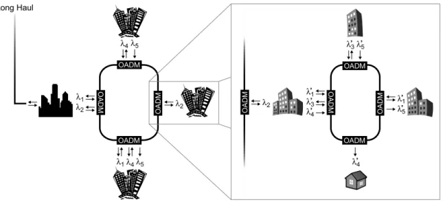
A modern optical ring-network is shown in Fig. 2.1. It is formed of interconnected rings of optical fiber. Each node of the optical network communicates with other nodes on dedicated wavelengths, also called channels. A node could be a building, a neighborhood or even a large town. The channels are all carried on the same optical fiber and densely space in a relatively narrow spectral band centered around 194 THz (free-space wavelength of 1550 nm). As of 2005, a single channel carries up to 40 Gb/s of data, which requires a minimum channel width of 40 GHz (~0.32 nm). The spectral-spacing between center-wavelengths of such consecutive channels can be as small as 100 GHz (~0.8 nm). This is referred to as dense wavelength-division multiplexing (DWDM). Obviously, there are many different DWDM schemes with diverse channel widths and channel spacings. Nonetheless, all schemes are limited to spectral bands defined by the operational spectral ranges of optical fiber amplifiers. First, the conventional band (C-band) is based on conventional Er-doped fiber amplifiers and spans a spectral window from about 1530 to 1565 nm. Then, the short band (S-band, 1460-1530 nm) is based on fiber Raman amplifiers and the long band (L-band, 1565-1625 nm)
is based on gain-shifted Er-doped fiber amplifiers [2]. The S- and L-bands have shown increasing interest in recent years but are not yet widely employed. The common goal is to fit as much bandwidth as is reasonably possible in a given spectral window with either numerous low-bandwidth tightly-spaced channels or fewer wider-bandwidth more-loosely-spaced channels.
Each node requires an optical add-drop multiplexer (OADM). An OADM is formed of a set of optical add-drop filters. As shown in Fig. 2.2, an add-drop filter must reroute (drop) the data stream carried at a given wavelength (λk) and replace it (add) by a new
data stream (λk’) carried at the wavelength that was just dropped. This must be done
without disturbing the other channels (λi≠k).
A spectral response of an add-drop filter is presented in Fig. 2.3. The response should be as square as possible. The input-to-drop loss, the loss on the adjacent channels and the ripple need to be minimized. On the other hand, the in-band extinction and the
Fig. 2.1 Schematic of a modern optical network employing interconnected rings of optical fiber. Each node of the optical network communicates with other nodes on dedicated wavelengths, which are also called channels. An optical add-drop multiplexer (OADM) is required at every node. An OADM is formed of a set of add-drop filters, which are described in Fig. 2.2.
out-of-band rejection need to be maximized. Usually, a ~3 dB drop loss is tolerated while only a ~1 dB loss on adjacent channels is found acceptable. The ripple introduces dispersion in the dropped channel and needs to be kept below ~0.1 dB. Dispersion can induce transmission errors by distorting the optical impulses forming the data stream. In general, dispersion is created by slope in the filter spectral response and should not exceed ~22 ps/nm. Power left in the through-port from the dropped data-stream (λk) will
act as noise for the added data-stream. Similarly, power rerouted to the drop-port from adjacent channels will act as noise for the dropped data-stream (if the dropped port is connected to a detector) or as noise for other adjacent channels (if the dropped data-stream is directed towards another optical fiber). Hence, the through extinction and the out-of-band rejection must both reach at least 30 dB.
For an OADM to be useful in practice, it has to fulfill two additional requirements. First, the spectral responses of the add-drop filters must be polarization independent. The polarization state in a fiber changes randomly. Any polarization dependence in the add-drop filters would means that their performance would change randomly in time. Second, the OADM should be reconfigurable. In other words, one should be able to drop any channel and output it on any of the OADM drop ports while the system is in use. This can be accomplished by using tunable add-drop filter, where the spectral response of the filter
Fig. 2.2 Add-drop-filter functionality. An add-drop filter must reroute (drop) the data stream carried at a given wavelength (λk) and replace it (add) by a new data stream (λk’)
carried at the wavelength that was just dropped. This must be done without disturbing the data streams carried on the other wavelengths (λi≠k).
Add - Drop Filter
Input Through Add Drop λ1… λk-1, λk, λk+1… λn λk’ λ1… λk-1, λk’, λk+1… λn λk
can be shifted and precisely positioned in the spectral domain over the entire spectral band used. Another approach is to use a complete set of switchable add-drop filters statically positioned on given channels. In this scheme, all add-drop filters are turned off but for the one corresponding to the channel to be dropped. Numerous other architectures are also possible. However, the heart of the challenge is creating an add-drop filter that is widely tunable or quickly switchable.
2.2 MICRORING-RESONATOR FILTERS 2.2.1 How They Work
Optical ring resonators were proposed in 1969 [3]. However, it was only in the late 1990s that fabrication advances made it plausible to consider these structures for add-drop filters. A microring resonator filter is shown in Fig. 2.4a. Let us imagine a monochromatic wave launched in the input port. The wave will evanescently couple to
Fig. 2.3 Spectral response of an add-drop filter. (a) Input-port to drop-port and add-port to through-port spectral response. (b) Input-port to through-port spectral response. An elliptic filter response is used in this illustration. [Calculation by M.A. Popovič]
the ring and start propagating in it. If the optical path length in the ring corresponds to an integer number of wavelengths, there will be resonance and a significant amount of power will be transferred to the ring. If the input and output coupling coefficient are properly chosen, nearly all optical power will be extracted from the input bus-waveguide and redirected to the drop-port. Each time a wave is evanescently coupled from one waveguide to another without significant coupler loss, it is phase shifted by 90 degrees with respect to the wave in the primary waveguide. Hence, the wave in the ring is 90 degrees phase shifted with respect to the wave in the input bus-waveguide. When the wave in the ring is resonant and couples back to the input bus-waveguide, the phase shift with the primary wave is mainly induced by the evanescent coupling, reaches 180 degrees, and results in destructive interference. Thus, after a short transient state, the optical power in the ring will have built up sufficiently to kill most of the wave in the through port. The microring filter exhibits two-fold rotational symmetry so the add function is accomplished in the same way as the drop function.
Fig. 2.4 (a) Schematic of a microring-resonator add-drop filter. (b) Spectral response of a single microring resonator. The spectral distance between resonances is called the free-spectral-range (FSR).
2.2.2 Spectral Response of Microring Filters
The spectral response of a single-microring filter is presented in Fig 2.4b. The spectral distance between two consecutive resonances is called the free-spectral-range (FSR). As only a single channel should be dropped at a time by a given add-drop filter, the FSR needs to be as wide as the spectral band used (usually 30 nm or more). The smaller the resonator is, the larger the spectral spacing between the resonances. The microring diameter needs to be on the order of 10 µm to provide an FSR on the order of 30 nm (this is dependent on the refractive index of the material used). Such small microrings require strong light confinement to manage bending loss. This is the primary reason for which high-refractive-index-contrast has to be used for microring filters.
The frequency selectivity of a single microring is most often measured through the quality factor of the resonator (Q). Q is defined as the time averaged stored energy per optical cycle divided by the power leaving the resonator. It is related to the wavelength selectivity through Q≈λ λ∆ where ∆λ is the full-width at half-maximum (FWHM) of
the resonance peak. Power leaving the resonator is due to scattering loss, material loss, and bending loss as well as to coupling to the bus waveguides. The smaller the couplings to the bus waveguides and the losses in the ring are, the longer the photon lifetime in the ring, the larger the Q, and the sharper the resonance. In short, the coupling strength defines the bandwidth of the filter as it, and not the losses in the ring, need to be the Q limiting factor (photon-lifetime limiting-factor) in add-drop filters.
An elegant way of looking at single-ring resonators is to reduce them to Fabry-Perot resonators. Accordingly, one considers the input and output waveguides as the Fabry-Perot mirrors. The transmission of the mirrors is equated to the evanescent coupling between the waveguides and the ring. In consequence, the spectral selectivity of a ring
resonator is sometimes described by its finesse (F) which is defined as F =FSR ∆λ
where ∆λ is the FWHM of the resonance peak.
A single microring forms a first-order filter, which yields a Lorentzian response. It is not square enough for DWDM applications, where a flat top and a sharp roll-off are required. These characteristics are obtained with appropriate high-order filters. A higher-order than first-higher-order microring filter can be obtained by arranging multiple microrings in a series-coupled configuration. A third-order microring filter requires three microrings and is presented in Fig. 2.5 along with the spectral responses of first-, second-, and third-order filters. By appropriate selection of the coupling ratios between the microrings, standard electronic filter responses such as Chebyshev, Butterworth, and elliptic can be obtained [4].
Fig. 2.5 (a) Schematic of a third-order microring resonator. (b) Drop-port response and (c) through-port response of first-, second-, and third-order microring filters [Calculation by M.A. Popovič]
In summary, the bus-to-ring couplings control the filter finesse (FSR/bandwidth), the ratios between bus-to-ring and the various ring-to-ring couplings control the filter shape, and the optical path lengths in the microrings (microring radius and optical propagation constant) control the resonant frequency and the FSR of the filter.
The optical propagation constant can be adjusted by changing the cross-section of the waveguides. It is most often expressed through the effective refractive-index of the waveguide defined as
0,
eff
n =β k
where β is the propagation constant and k is the free-space wavenumber. These two 0 quantities are defined through
( ) 0 0 0 ( , ) and 2 , i t z E z t E e k ω β π λ − = =
where E is a given electric-field component of the propagating wave, z is the propagation direction of the wave, λ0 is the free-space wavelength, and ω is the radial frequency. For more information on optical wave propagation in dielectric media please refer to [5].
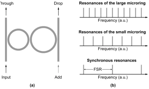
2.2.3 Racetrack Resonators and Vernier Operation
Racetrack resonators and Vernier operation have attracted significant attention in the literature. However, neither was employed in the present work as their drawbacks were found to outweigh their benefits.
Racetrack resonators are elongated rings created by introducing straight segments as shown in Fig 2.6. They are used to ease restrictions on the coupling regions. Coupling gaps in microring resonators can be narrower than 0.1 µm, which requires use of
expensive high-resolution lithography. For a given coupling coefficient, the coupling gaps are wider for racetracks than for rings as the coupling region is longer. This eases lithographic requirements. Nonetheless, the straight portions increase the path length in the resonator significantly and, in turn, reduce the FSR appreciably. To restore the FSR, a higher index-contrast must be used. A higher index contrast means stricter lithographic requirements and the racetrack’s main benefit is partially lost. In addition, the optical mode in a bend is spatially offset in the waveguide towards the outer radius. Connecting a straight waveguide to a bent waveguide results in modal mismatch and, consecutively, in optical loss. To manage this problem, smooth transitions or accurate waveguide offsets need to be introduced.
Vernier operation can significantly enlarge the FSR of coupled-resonator filters. Enlarging the FSR enables a lower index-contrast to be used to achieve the required filter specifications. A lower index-contrast relaxes fabrication tolerances and reduces scattering losses. Each microring shows a comb of resonances. Two microrings with different radii (hence different FSR) in a series-coupled configuration will form a second-order filter with an enlarged effective FSR. As illustrated in Fig 2.7, the filter will drop power only at frequencies where both microrings are resonant (synchronous resonances).
Fig. 2.6 Schematic of a racetrack-resonator add-drop filter. Straight segments are introduced to enhance coupling to the bus waveguides and allow wider coupling gaps than in microring resonators. Smooth curvature transitions or precise offsets need to be introduced to reduce loss resulting from mode mismatch between straight and bent waveguide segments.
Superimposing the combs of resonances of both microrings, the effective FSR of the filter will be the distance between the spectral positions where resonances of both microrings overlap.
The Vernier effect was successfully employed to extend the FSR of drop-only filters [6] where the through response is not critical. However, it cannot be used for add-drop filters as it can introduce intolerable dispersion in the through port. At spectral positions where the input ring is resonant but not the output ring, the filter acts as a single ring connected only to the input bus-waveguide. Such a filter is called an all-pass filter. It can introduce loss and intolerable dispersion at the input-ring resonances that do not correspond to output-ring resonances.
Fig. 2.7 (a) Schematic of a second-order microring-filter employing the Vernier effect. (b) Illustration of the Vernier effect. Power will be dropped only at frequencies where both microrings are resonant (synchronous resonances).
Fabricated Add-Drop Filters
3.1 INTRODUCTION
The present Chapter is an overview of the fabrication work done to realize the most advanced microring add-drop-filters reported in the literature. It allows demonstrating problems encountered in the fabrication of HIC filters and motivating Parts II and III of the Thesis. The reader is referred to later Chapters for detailed investigations of given problems. As mentioned in Chapter 1, microring resonators are a good example of high-index-contrast (HIC) microphotonic devices. In this Chapter we demonstrate fabrication problems that need to be addressed in HIC devices in general.
The filters were fabricated in four distinct phases that are reported in Sec. 3.4. An overview of the structures and of the fabrication process is presented in Sec. 3.2 and 3.3. Finally, a scheme allowing doubling the free-spectral-range (FSR) of microring filters is demonstrated in Sec. 3.5.
3.2 STRUCTURES OVERVIEW
Our goal was to create add-drop filters with a 40 GHz bandwidth, less than 0.1 dB ripple, at least 20 nm of FSR, and at least 30 dB of in-band extinction and out-of-band rejection
(assuming a 100 GHz channel spacing). Consequently, third-order filters were designed with a flat-top (Chebyshev) drop-port response using known synthesis techniques [4]. The coupling gaps were obtained using three-dimensional finite-difference-time-domain (3D FDTD) simulations [7]. The design strategy is reported in [8], [9] and [10]. For a detailed treatment of the filter design and numerical simulations, the reader is referred to [7] and [11].
A series-coupled third-order microring filter is shown schematically in Fig. 3.1. The waveguides are formed of a silicon-rich silicon-nitride (SiN) core, a silicon-oxide under-cladding, and an air top-cladding. The waveguides are designed monomode. Hence, they support a single TE-like (main E component horizontal) and a single TM-like (main E component vertical) mode only. The mode used in all microrings presented below is the TE-like mode. Polarization independence is addressed in Sec. 3.4.4. The waveguides are designed wide and flat
1. to reduce the field overlap at the sidewalls to lower scattering losses due to sidewall roughness and decrease the sensitivity of the effective index (and, hence, of microring resonant frequencies) to the waveguide width, and
2. to induce modal birefringence (effective-index difference between TE- and TM-like modes) to avoid waveguide-imperfections induced coupling between polarizations.
Designed filter dimensions are summarized in Table 3.1 for all fabricated third-order filters. Unless otherwise indicated, all refractive indices in the present work are reported for λ0 =1.55 µm. FSR-doubling of microring filters was demonstrated on second-order filters described in Sec. 3.5.
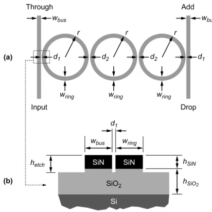
Fig. 3.1 Schematic of a series-coupled third-order microring filter. The microrings are designed identical. The actual parameters used are presented in Table 3.1. (a) Top view. (b) Cross-section of the waveguides at the bus-to-ring coupling region.
TABLE3.1
DESIGNED THIRD-ORDER-FILTER PARAMETERS
Parameter First Third-Order Filters First Frequency-Matched Filters Multistage Filters Independent Filters Polarization
hSiN 330 nm 400 nm 396 nm 420 nm hSiO2 2.5 µm 3 µm 3 µm 3 µm hetch 430 nm 500 nm 600 nm 520 nm nSiN 2.200 2.200 2.181 2.193 nSiO2 1.445 1.455 1.455 1.455 wbus 850 nm 804 nm 702 nm 600 nm wring 1050 nm 804 nm 900 nm 876 nm d1 60 nm 102 nm 120 nm 162 nm d2 285 nm 492 nm 372 nm 396 nm r 7265 nm 8004 nm 7998 nm 7998 nm
But for the first third-order filters, all lithographically defined dimensions were rounded to a 6 nm scanning-electron-beam-lithography step-size to ensure consistent discretization of patterns.
3.3 ONE-LAYER FABRICATION PROCESS
Fabrication of HIC microring resonators requires high-resolution lithography, strict dimensional control, and smooth sidewalls. Consequently, the fabrication process is based on direct-write scanning-electron-beam lithography (SEBL) and non-chemically-amplified resist.
A process diagram is shown in Fig. 3.2. First, a Si wafer is thermally oxidized to form a 2.5- to 3-µm-layer of SiO2. Then, a 330- to 400-nm-layer of SiN is deposited by
low-pressure chemical-vapor-deposition (LPCVD) in a vertical thermal reactor with a gas mixture of SiH2Cl2 and NH3 in a 10 to 1 ratio. The resulting SiN shows low stress and is
often referred to as low-stress nitride. The vertical thermal reactor provides excellent on-wafer uniformity and a repeatable on-wafer-to-on-wafer distribution of film thicknesses and
Fig. 3.2 Fabrication process overview (a) Initial multilayer formed of 3 µm of silicon oxide, 400 nm of silicon-rich silicon-nitride (SiN), 200 nm of poly-methyl-methacrylate (PMMA) and 60 nm of Aquasave [12]. (b) Scanning-electron-beam-lithography exposure, Aquasave removal, and PMMA development. (c) 45 nm Ni evaporation. (d) Liftoff. (e) Reactive-ion etching and Ni removal.
indices of refraction. The most suitable wafer for device fabrication is selected from the batch by measuring the obtained thicknesses and indices of refraction with a spectroscopic ellipsometer. Next, 200 nm of poly-methyl-methacrylate (PMMA) and 60 nm of Aquasave are spun on. PMMA is a positive e-beam resist while Aquasave [12] is a water-soluble conductive polymer used to prevent charging during SEBL. The PMMA is exposed at 30 KeV using a Raith 150 SEBL system. The Aquasave is removed, and the PMMA developed. Next, a 45- to 50-nm-layer of Ni is evaporated on the structure, and a liftoff performed by removing the non-exposed PMMA. Using the Ni as a hardmask, the waveguides are defined by conventional reactive-ion-etching (RIE) with a gas mixture of CHF3-O2. To obtain an accurate etch depth, the RIE is performed in
several steps, between which the etch depth is measured with a profilometer. Finally, the Ni is removed using a nitric-acid-based commercial wet Ni etchant and the sample prepared for optical characterization.
The fabrication process is optimized to reduce sidewall roughness as described in Fig. 3.3 Cross-section of a smooth SiN waveguide. The desired etching depth was 430
nm. A 10 nm etch depth accuracy is obtained by performing the RIE in several steps, between which the etch depth is measured with a profilometer.
Chapter 5. Moreover, strict dimensional control is achieved by process calibration as described in Chapter 8. The cross-section of a resulting fabricated waveguide is presented in Fig. 3.3. Using this process, ring-to-bus gaps as small as 50 nm were successfully fabricated with good repeatability. Note that the polarization-independent filters require a more complex two-layer fabrication process that will be presented in Sec. 3.4.4.
3.4 FABRICATED THIRD-ORDER FILTERS 3.4.1 First Third-Order Filters
The goal of the first third-order filters was to create a wide variety of structures to asses the partially optimized fabrication process and the initial designs. The filters were fabricated as described in Sec. 3.3. The designed dimensions are reported in Table 3.1. A fabricated filter along with the experimental layout is presented in Fig. 3.4. As a wide variety of filters were fabricated, the structures were only coarsely calibrated. Nevertheless, a 20 nm dimensional control was achieved. Detailed dimensional measurements are presented in Chapter 8.
The measured vertical waveguide parameters are reported in Table 3.2. The discrepancy between the designed and the employed SiN thickness is due to a problem with the optical characterization tool (single-angle narrow-spectral-band spectroscopic ellipsometer) used in the clean room to select the device wafer. More accurate measurements were obtained using a Sopra spectroscopic ellipsometer with multi-angle measurements and wide (400-2000 nm) spectral scans. Both the SiN and SiO2 refractive
indices were higher than expected. For SiN this is easily understood as the reactants are introduced in a strongly non-stoichiometric ratio to create a silicon-rich material. Hence, the material composition is sensitive to deposition parameters and the index is expected
to vary from batch to batch. For thermal oxidation of Si, however, it is usual to get variations in the film thickness but not in the refractive index. The refractive index offset was found to be repeatable and is most likely due to Si dopants that become part of the SiO2 once the Si is oxidized.
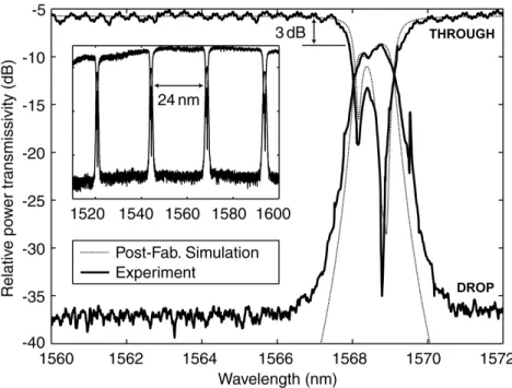
The filter response is presented in Fig. 3.5. For the first time, a low drop loss (3dB) and a wide FSR (24 nm) were demonstrated in high-order HIC filters without using the Vernier effect. The drop loss was improved by 10 dB over previously reported wide-FSR
Fig. 3.4 Third-order add-drop filter based on series-coupled microring resonators. (a) Scanning-electron micrograph. (b) Schematic of the chip layout used in the experiment. To ensure a reliable drop-loss measurement, the drop and the through waveguides traverse equivalent paths.
filters [13]. The FSR was improved by more than a factor of 2 over moderate-index-contrast filters with only a 2 dB penalty in the drop-loss [14].
Post-fabrication simulations were performed to understand the observed response of the fabricated third-order filter using the measured dimensions and refractive indices. Ring-ring and ring-bus coupling coefficients were calculated using 3D FDTD. A cylindrical mode solver yielded bend losses and ring effective and group indices. The ring resonant frequencies were chosen to fit the data. As seen in Fig. 3.5, the spectral response of the filter is matched to excellent agreement by the rigorous numerical simulations.
The FDTD simulations indicate that additional losses were present in each of the rings due primarily to coupling to a lossy higher-order transverse mode of the ring waveguide at the couplers. The waveguides support a single mode of each polarization when straight, but when bent regain the second-order TE mode as a leaky resonance with high bend loss. A higher-order mode can be tolerated if its loss is engineered to be high enough to ensure that it is not resonant and that no coupling to it from the fundamental mode is present. In our design, the bending loss of the second-order TE mode was sufficient to suppress its resonance but too low to forbid its excitation at the couplers by
TABLE3.2
VERTICAL WAVEGUIDE PARAMETERS OF FIRST THIRD-ORDER FILTERS
Parameter Designed Measured
hSiN 330 nm 314 ± 1 nm
nSiN 2.200 2.217± 0.006
hSiO2 2.50 µm 2.53 ± 0.01 µm
nSiO2 1.445 1.455 ± 0.003
hetch 430 nm 440 ± 10 nm
Layer thicknesses and indices of refraction were measured with a Sopra spectroscopic ellipsometer, while the etch depth was measured with a Dektak profilometer.
the fundamental resonance. This excitation translates to coupler losses, which are higher in the outer rings since the ring-bus coupling is stronger than the ring-ring coupling. This coupler scattering is a significant loss mechanism. Coupler scattering and bend loss fully account for the observed 3 dB drop loss. Hence, scattering loss and material loss have no impact on the performance of the present filter. The propagation loss in straight waveguides was measured using the Fabry-Perot method. In short, the waveguide is considered as a Fabry-Perot resonator with the Fabry-Perot mirrors being formed of the reflections at the waveguide input and output facets. The Q of the resonator will be limited by propagation loss of the waveguide and the transmission at the waveguides facets. A propagation loss of 3.6 dB/cm was obtained. This loss was later found to be strongly under-estimated because of the strong sensitivity of the measurement to changes in the reflectivity of the waveguide facets. More accurate propagation loss measurements were obtained in analysis of later fabrication phases. An investigation of propagation loss in SiN waveguides is presented in Sec. 6.7.4.
The SEBL field covers a 100 100 µm× area. Features larger than a single field require exposing multiple fields and moving the interferometrically-controlled SEBL stage between the field exposures. A field-stitching error with zero mean and 20 nm standard deviation is expected. In the present filters, a rotational error in the SEBL field calibration created a 30 nm mean offset of the bus waveguides every 100 µm. Numerical simulations indicate that such offsets result in a significant loss of 0.021 dB/junction or 2.1 dB/cm. This illustrates the sensitivity of HIC waveguides to any perturbation.
The spectral asymmetry, clear in the through-port response of Fig. 3.5, is indicative of unequal, symmetrically distributed resonance frequencies, with the central ring having a higher frequency than the outer rings by 22 GHz. The effect is partially explained by coupling-induced frequency shifting (CIFS) of resonators [15], a purely optical effect due
to the index perturbations caused by adjacent ring and bus waveguides. The CIFS calculated by FDTD for the present filters is 43 GHz. Frequency shifts also result from dimensional variations in the rings due to e-beam proximity effects, SEBL discretization errors and other lithographic imperfections such as SEBL digital-to-analog converter errors. The frequency mismatch is corrected in later fabrication phases and the correction mechanism is thoroughly described in Chapter 9.
Despite accurate dimensional control at fabrication, the measured 88 GHz bandwidth was more than twice the intended 40 GHz bandwidth. Matching of post-fabrication simulation results and experimental data supports the validity of the simulations, and the discrepancy is attributed to the simple couple-mode-theory model used in the design.
Fig. 3.5 Measured and simulated response of the first third-order microring filters. The spectral asymmetry is due to frequency mismatch of resonators and can be compensated. Input-to-drop loss is dominated by scattering at the 60-nm-wide ring-bus coupler gaps. The narrow peak on the right of the drop spectrum is a measurement artifact. The inset shows several resonances and the free-spectral-range. [Measurement by P.T. Rakich, simulations by M.R. Watts and M.A. Popovič]
Finally, a larger-than-intended passband ripple limited in-band (through-port) extinction to 9 dB instead of an intended 13 dB. The resonant frequency mismatch further reduced this to 7.5 dB.
3.4.2 First Frequency-Matched Filters
In the first third-order filters, the following three problems were identified: 1. inaccurate bandwidth,
2. coupler loss,
3. frequency mismatch of resonators.
In the second fabrication phase, these three problems were addressed. The bandwidth and the coupler loss were improved by using rigorous 3D FDTD simulation to redesign the waveguide cross-section and the coupler gaps [8]. The frequency mismatch was corrected by a deliberate increase of the SEBL dose on the middle microring. Such a dose increase results in a slightly wider middle-ring-waveguide and lowers the resonance frequency of the middle ring to match it to the outer rings. The frequency-matching technique is described in Chapter 9.
The filters were fabricated as described in Sec. 3.3. The process was properly calibrated to achieve strict dimensional control as described in Chapter 8. Dimensional measurements are reported in Sec. 8.3 and Sec. 9.6. The SEBL writing strategy was optimized to achieve smooth rings with a uniform ring-waveguide width. The SEBL writing strategy is addressed in Chapter 7.
Fig. 3.6 (a) Micrograph of a frequency-matched filter. (b) Measured and fit spectral response of a filter without dose-compensation. A 170 GHz mismatch is observed. (c) Filter that is frequency-matched to better than 1 GHz as a result of an intentional SEBL dose increase of 4.5% on the middle ring. [Measurement by P.T. Rakich, simulations by M.A. Popovič and M.R. Watts]
A micrograph of a frequency-matched filter is shown in Fig. 3.6a. The spectral responses obtained with and without SEBL dose compensation are shown in Fig. 3.6c and Fig. 3.6b, respectively. The uncompensated filter shows a frequency mismatch of 170 GHz with 38 GHz attributed to CIFS (from 3D FDTD simulations). This is much higher than the 22 GHz frequency mismatch in the first third-order filters. The difference is mainly due to
1. uniform SEBL discretization of patterns obtained in the present filters by choosing all dimensions to be multiples of the SEBL step size (discretization errors may have introduced a significant negative frequency shift component in the first third-order filters), and to
2. a difference in ring-waveguide width between the two designs, making the resonant frequency of the present filters twice as sensitive to waveguide-width variations as the first third-order filters.
The three microring resonators of the best compensated filter are frequency matched to better than 1 GHz (5 ppm). This allowed the in-band extinction to reach 14 dB, the highest reported in the literature. Since the resonance frequency of these microrings changes by about 40 GHz for a change of 1 nm in the average ring-waveguide width, the average waveguide-widths of the three microrings are matched to better than 26 pm to a desired width-offset needed to compensate for the CIFS. Obtaining such relative dimensional control is addressed in Chapter 9. These filters were the first frequency-matched microring filters reported in the literature.
The main downside of the present filters is the high drop-loss (5-6 dB). From the filter responses, the propagation loss is estimated to 10-15 dB/cm. This is the main source of loss in the filters as bending and coupler loss are responsible for only 1.5 dB of drop loss. At first, the higher than expected propagation loss was attributed to an imperfect Ni
liftoff. The Ni evaporation produced a thicker film (62 nm) than expected (45 nm) and a coarse microstructure, which amplified the line-edge-roughness of the Ni hardmask and translated to larger sidewall roughness and higher than expected scattering losses. To reduce scattering losses in later fabrication phases, the process was carefully re-optimized to minimize roughness. The optimization strategy and resulting roughness are reported in Chapter 5. Nonetheless, the scattering loss analysis of Chapter 6 and later experiments have shown that the propagation loss should rather be attributed to SiN material loss. This is discussed in Sec. 6.7.4.
The 1 dB bandwidth of the frequency-matched filters is 30 GHz. The designed filter bandwidth is 38 GHz. The discrepancy is attributed to rounding of the filter response due to propagation loss and to lower than expected coupling coefficients. The later are mainly due to a slight offset of the actual SiN refractive index and thickness from design values. The designed and measured vertical dimensions are shown in Table 3.3. The SiN layer of the device wafer cannot be directly characterized prior to fabrication as the adequate characterization tool (Sopra ellipsometer) is not located in a clean environment. The device wafer is selected from a deposition batch by accurately characterizing monitor wafers placed on the edges of the stack and interpolating the SiN thickness and index of refraction on the remaining wafers. Variations in the deposition rate and film composition
TABLE3.3
WAVEGUIDE VERTICAL PARAMETERS OF
FIRST FREQUENCY-MATCHED FILTERS
Parameter Designed Measured
hSiN 400 nm 406 ± 1 nm
nSiN 2.200 2.189 ± 0.003
hetch 500 nm 510 ± 10 nm
SiN thickness and index of refraction were measured with a Sopra spectroscopic ellipsometer, while the etch depth was measured with a Dektak profilometer.
does not allow for accurate control of thickness and refractive index at MIT. In later fabrication phases, the design was trimmed to the interpolated SiN index and thickness of a chosen device wafer prior to fabrication.
3.4.3 Multistage Filters
Add-drop filters have to provide an in-band extinction of at least 30 dB. Even if a third-order filter were perfectly fabricated, its in-band extinction would only reach about 20 dB. To obtain the required extinction with a single filter, a filter of higher order than third would be required. When the order of a filter is increased, the fabrication tolerances become more stringent. Another possible approach to reach the required in-band
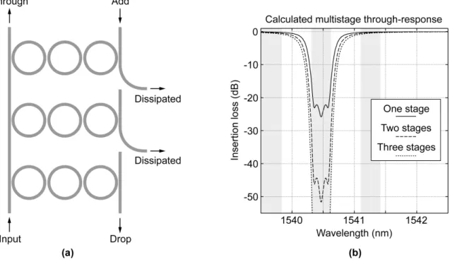
Fig. 3.7 Cascaded third-order filters used to enhance the in-band extinction. (a) Three-stage third-order filter. The power dropped at the second and third Three-stage is dissipated. (b) Calculated through-port spectral response of one-, two-, and three-stage filters. The in-band extinction of a multistage filter is the sum (in dB scale) of the in-in-band extinctions of the individual stages forming the filter. [Scheme proposed by M.A. Popovič]
extinction is to cascade third-order filters as shown on Fig. 3.7. Such a multistage filter introduces new degrees of freedom in filter design and allows decoupling the design of the drop-port response from the design of the through-port response. Consequently, the through-port response can be improved without increasing the drop-loss and making fabrication tolerances more stringent. The in-band extinction of a multistage filter is given by the sum (in dB scale) of the in-band extinctions of the individual stages forming the multistage filter.
The main fabrication challenge in cascading filters is to have all stages spectrally
Fig. 3.8 Fabricated multistage filters. (a) Electron micrograph of one, two- and three-stage filters showing the layout used in the experiment. (b) Electron micrograph of a single stage.
aligned to within a few GHz. Thus, the stages must be kept spatially close to one another to prevent resonant frequency variations due to non-uniformity in the SiN thickness, SiN index, PMMA thickness, and development rate. Moreover, the stages need to be e-beam written with minimal time delays between the stages to avoid drift of the e-beam current in between stage exposures (a dose difference would result in a frequency difference). However, it would be ill-advised to put all stages in the same SEBL field. Rather, the stages are exposed in consecutive SEBL fields and positioned in the center of each field to avoid spectrally misaligning the filters by SEBL intra-field distortions.
The filters were fabricated as described in Sec. 3.3. The fabrication process was optimized to minimize sidewall roughness as presented in Chapter 5. The filters were re-designed for the SiN index and thickness of a selected device wafer. An asymmetric coupler design reduced coupler scattering significantly when compared to the first frequency-matched filters. This provided for a better tolerance of the filter spectral response to propagation loss. The designed filter parameters are presented in Table 3.1.
A micrograph of fabricated one-, two-, and three-stage third-order filters is presented in Fig. 3.8. The spectral response of a one- and two-stage filter is presented in Fig. 3.9. The dose-compensated one-stage filter is frequency-matched to better than 2 GHz and shows an in-band extinction of 17.5 dB, the highest reported in literature (the previously highest extinction was that of the first frequency-matched filters). The average ring-waveguide widths are matched to better than 68 pm to a desired width-offset within a single stage. The filter 1 dB bandwidth is 42 GHz, only 2 GHz off the designed 40 GHz bandwidth. The drop loss was improved to 2.5 dB as a result of the asymmetric coupler design. The propagation loss remained high near 10 dB/cm despite smoother waveguide-sidewalls. Roughness measurements were performed using the method presented in Chapter 4 and are reported in Sec. 5.4. The continuation of the high propagation loss
despite improvement of sidewall roughness suggests that scattering losses are not the main source of loss. This was confirmed by the analysis of Chapter 6 and is addressed in Sec 6.7.4.
The in-band extinctions of two- and three-stage filters are limited by a -30 dB
Fig. 3.9 Spectral response of (a) a one-stage filter and (b) a two-stage filters. The in-band extinction of the two- and three-stage filters is characterization-limited to 30 dB by the laser line of the tunable laser used for characterization. The noise floor in the drop-ports is not limited by the laser line and reaches -40 dB. [Measurement by P.T. Rakich and L. Socci, design by M.A. Popovič, and required FDTD simulations by M.R. Watts]
characterization noise-floor most likely due to the laser line of the tunable laser used at characterization. This noise floor does not allow appropriate characterization of the through-port response but is sufficient to demonstrate that the in-band extinction reaches the required 30 dB. Note that the drop-port noise-floor is not laser-line limited and reaches about -40 dB.
The stages were spectrally aligned within 2 to 5 GHz. For a three-stage filter, this indicates that the average ring-waveguide widths of all 9 rings are matched to the ideal to better than 0.16 nm. The drop-port responses of the three consecutive stages of a three-stage filter are shown in Fig. 3.10. The responses are well aligned, symmetric, and follow the theoretically predicted shape. Even if a higher than 30 dB extinction is not desired, a triple-stage filter may still be found desirable. It relaxes fabrication tolerances by
Fig. 3.10 (a) Measured and (b) calculated spectral responses at drop-ports of successive stages of a three-stage filter. The measured spectral responses are consistent with the calculated ones. The stages are spectrally aligned within 2-5 GHz. The higher noise-floor in the third drop-port measured is most probably due to a problem with the end-facet at the output of the chip. [Measurement by P.T. Rakich and L. Socci, calculation by M.A. Popovič]
allowing a wide range of dose-compensation to provide the required 30 dB extinction. This is further addressed in Chapter 9.
3.4.4 Polarization-Independent Filters
3.4.4.1 Integrated Polarization Diversity
All microring filters presented above work for the TE polarization only (main E component in the plane of the substrate). However, the polarization state in an optical fiber is random and both polarizations need to be handled equally. Polarization independent HIC filters, showing identical spectral responses for TE and TM polarizations, are not achievable in practice as they require control of dimensions and indices of refraction that may not be available for years to come. To achieve polarization-independent operation in HIC filters, we turn instead towards an integrated polarization diversity scheme [7,16]. As presented in Fig. 3.11, the polarization is first split in its TE and TM components. Then, the TM is rotated to become TE and both arms go through identical copies of the same filters. Finally, the non-rotated TE is rotated to become TM and the two arms are combined near the output of the chip. In this way, a
polarization-Fig. 3.11 Integrated polarization-diversity scheme allowing for polarization-independent optical chips built from polarization-dependent components. The input polarization is split in its TE and TM components. The TM is then rotated to become TE and both arms go through identical optical elements. The non-rotated TE is rotated to become TM and the two polarizations are combined at the output. [Scheme by M.R. Watts and H.A. Haus]
independent optical chip can be formed from polarization-dependent optical elements. The rotation of the TE into TM at the end of the chip is required to avoid creating an interferometer between the two polarizations and to have perfectly balanced arms. The combiner is simply a splitter used in reversed direction.
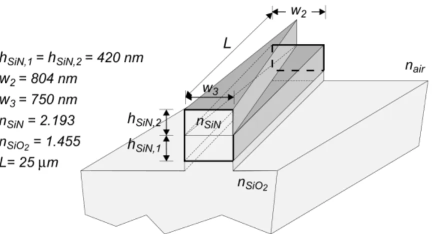
The needed integrated polarization splitters and rotators (PSR) were designed employing adiabatic mode evolution [7, 17, 18]. In other words, there is no mode coupling in the structure. Instead, a single mode is used for each polarization. The mode is slowly transformed to achieve polarization splitting and rotating. This approach makes the PSR tolerant to fabrication errors. The PSR design is shown in Fig. 3.12. To ensure appropriate characterization of the device, polarization-independent couplers were designed and are presented in Fig. 3.13.
Fig. 3.12 Integrated polarization splitter and rotator. The structure can be anywhere between 300- to 600-µm-long. A longer structure allows for more relaxed fabrication tolerances. The design parameters are reported in the upper left. [Design by M.R. Watts]
3.4.4.2 Two-Layer Fabrication Process
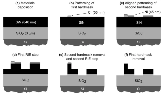
The PSR is a two-layer structure. The lower layer is shared with the microring filters. To simplify the fabrication process, we proposed an innovative multilayer processing approach depicted in Fig. 3.14 [19]. First, the full SiN thickness of the two layers is deposited. Then, the top-layer pattern is exposed and the pattern transferred into a Cr hardmask by liftoff. Next, the bottom-layer pattern is exposed and the pattern transferred into a Ni hardmask by liftoff. The bottom-layer exposure is aligned to the top-layer pattern registered in the Cr hardmask. The structure is RIE etched halfway, the Ni hardmask removed, and the structure RIE etched again. Finally, the Cr hardmask is removed and the samples are prepared for optical characterization.
The RIE is done iteratively as described in Sec. 3.3. However, a gas mixture of CHF3-O2 in a 16-to-4 sccm ratio is used (16-to-3 ratio used in the one-layer process) to
prioritize vertical sidewalls in the high-aspect-ratio structures over sidewall smoothness. Fig. 3.13 Polarization-independent fiber-to-chip coupler required for polarization-independent operation. The initial waveguide cross-section allows for equal coupling efficiency of the fundamental TE- and TM-like modes. The waveguide is initially multimode but any initial higher-order mode is radiated at the taper. [Design by M.R. Watts]
The first etch defines the height of the bottom layer while the second etch defines the height of the top layer. Hence, the first etch must take into account the required over-etch into the SiO2 and the etch rate difference between the SiN and the SiO2 during the second
etch. The second etch is done at reduced bias (300 V instead of 500 V) until the SiO2
boundary was reached to avoid erosion of waveguide corners in the bottom layer that is transferred down without a mask. When transferred down without a mask, the structure width is thinned down by up to 100 nm. Each sidewall is moved inwards horizontally by up to 1 nm for every 10 nm etched vertically. This reduces the effective resolution on the bottom layer by the amount of thinning encountered. For this reason the filter coupling
Fig. 3.14 Novel multilayer fabrication process used for the polarization independent add-drop-filters. (a) The full SiN thickness is deposited by LPCVD. (b) The pattern of the top layer is registered into a Cr hardmask using e-beam lithography and liftoff. (c) The pattern of the bottom layer (layer of the filters) is registered into a Ni hardmask using aligned e-beam lithography and liftoff. (d) The first RIE step defines the height of the bottom layer. (e) The second RIE step defines the height of the top and bottom layer. (f) The remaining Cr hardmask is removed.
region was redesigned to enlarge the coupling gap to 162 nm. Moreover, the two layers need to be carefully and independently optimized and dimensionally calibrated, as described in Chapters 5 and 8, for the wide range of dimensions needed (70 to 3000 nm).
The minimum feature size used was 70 nm. Below it, the 940-nm-tall waveguides (aspect ratio of 13.5-to-1) were mechanically unstable during wet processing. Cross-sections of resulting etched structures are presented in Fig. 3.15. The SEBL alignment procedure enables alignment accuracy with standard deviation of 20 nm or better. It is described in Appendix I.
The Ni hardmask can be removed without damaging the Cr hardmask by using a nitric-acid based commercial wet etchant (Transene TFB). The Cr hardmask is stripped at the end of the process with a perchloric-acid based commercial wet-etchant (Cyantek CR-7). The hardmask-material order is important as Cr cannot be easily removed without
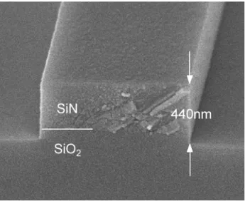
Fig. 3.15 Electron micrographs of waveguide cross-sections obtained using the fabrication process presented in Fig. 3.14. (a) Tall waveguide spanning the top and bottom layer of the structure. (b) Waveguide on the bottom layer of the structure. Sharp edges are obtained in bottom-layer waveguide by reducing the RIE power at the second RIE step, when the bottom layer is transferred down without a mask. Sidewall roughness is worse in these micrographs than in Fig. 3.2 as the RIE was optimized for vertical sidewalls and not sidewall smoothness. In addition, the roughness on the tall waveguide is worse than on the bottom-layer waveguide as ultrasonic agitation is used for Cr liftoff. This is addressed in Chapter 5.
![Fig. 3.2 Fabrication process overview (a) Initial multilayer formed of 3 µm of silicon oxide, 400 nm of silicon-rich silicon-nitride (SiN), 200 nm of poly-methyl-methacrylate (PMMA) and 60 nm of Aquasave [12]](https://thumb-eu.123doks.com/thumbv2/123doknet/13828730.443103/38.918.219.701.601.925/fabrication-process-overview-initial-multilayer-silicon-methacrylate-aquasave.webp)