HAL Id: hal-00945302
https://hal.archives-ouvertes.fr/hal-00945302
Submitted on 18 Feb 2014
HAL is a multi-disciplinary open access
archive for the deposit and dissemination of
sci-entific research documents, whether they are
pub-lished or not. The documents may come from
teaching and research institutions in France or
abroad, or from public or private research centers.
L’archive ouverte pluridisciplinaire HAL, est
destinée au dépôt et à la diffusion de documents
scientifiques de niveau recherche, publiés ou non,
émanant des établissements d’enseignement et de
recherche français ou étrangers, des laboratoires
publics ou privés.
Electro-magnetic robustness of integrated circuits: from
statement to prediction
Sonia Ben Dhia, Alexandre Boyer
To cite this version:
Sonia Ben Dhia, Alexandre Boyer. Electro-magnetic robustness of integrated circuits: from statement
to prediction. 2013 9th Intl Workshop on Electromagnetic Compatibility of Integrated Circuits (EMC
Compo 2013), Dec 2013, Nara, Japan. pp.208 - 213, �10.1109/EMCCompo.2013.6735202�.
�hal-00945302�
Electro-Magnetic Robustness of Integrated Circuits:
from statement to prediction
S. Ben Dhia, A. Boyer
LAAS-CNRSUniversité de Toulouse ; UPS, INSA, INP, ISAE ; UT1, UTM, LAAS Toulouse, France
Abstract - EMRIC project, a new research activity mixing
integrated circuits electromagnetic compatibility (EMC) and integrated circuits (ICs) reliability, provides methods and guidelines to circuits and equipment designers to ensure EMC during lifetime of their applications. In order to improve the ICs electromagnetic robustness (EMR) this project studies the effect of ICs ageing on electromagnetic emission and immunity to radio frequency interferences, clarifies the link between IC degradations and related EMC drifts and develops prediction models and propose “time insensitive” EMC protection structures.
Keywords: Integrated circuits, electromagnetic compatibility, reliability, robustness, accelerated aging, EMC modelling
I. INTRODUCTION
Introducing new high performance electronic modules in automotive, aeronautic and aerospace applications forces system manufacturers to optimize system reliability and reduce time to market delivery and manufacturing costs. This trend has triggered off an increasing demand for conclusive statements about future lifetime and function of the product already at the design stage, ranging from electromagnetic effects (EMC/RF) to thermal management issues and thermo-mechanical reliability forecasts.
Technological evolution of CMOS technologies brings a shrink of dimensions, a better integration rate and an enhancement of performances such as switching speeds. However it also leads to an increase of dissipated power and leakage current that have a direct impact on ICs parasitic emissions. Moreover reduced supply voltages and an increased number of interfaces tend to decrease the immunity to radio-frequency interference. EMC has become a major concern and a key differentiator in overall IC performance [1] [2].
During their lifetime, integrated circuits may be affected by failure mechanisms mainly activated by harsh environmental conditions (high or low temperature, humidity, vibration, electrical overstress…). The acceleration of intrinsic
degradation mechanisms in nanoscale devices threats the reliability of circuits [3]. Even if failure mechanisms do not compromise the circuit operation, IC intrinsic degradations can have a significant impact on EMC performances. The need to predict EMC of ICs after several years of operating life is driven by the trend towards extended warranty. Ensuring the electromagnetic robustness of nanoscale integrated circuits (extension of the electromagnetic compatibility for the full lifetime of the product) has become a key challenge.
EMRIC project aimed at developing a new research activity that mixes EMC and IC reliability to improve the electromagnetic robustness of integrated circuits, with a special emphasis on deep submicron technology. This research topic is still under-explored as research communities on “IC reliability” and “IC electromagnetic compatibility” have often no overlap. The effect of natural aging of ICs on their electromagnetic behavior is still misevaluated and has to be clarified. Highlighting the EMC drift issues induced by IC natural aging, understanding the links between the physical degradation mechanisms induced by ICs aging and EMC drifts, predicting the extent of aging induced EMC drifts and providing guidelines to design robust EMC protection structures are the main objectives of this project.
The first part of the paper presents the methodology set up to study the evolution of ICs electromagnetic behavior over the full lifetime of the component. The second part, dedicated to experimental results, exhibits the drifts of a test chip electromagnetic emission and immunity levels and the link between degradation mechanisms and transistors physical parameters drifts that affect EMC. In the last section, a modeling and simulation approach is proposed.
II. EMRMETHODOLOGY
The characterization of the EMR of a circuit consists in measuring its emission and/or susceptibility level before and after ageing procedures that accelerate intrinsic degradation mechanisms. The main objective of this study is to evaluate electromagnetic drifts as function of stress types, stress
conditions and stress duration. Figure 1 presents the methodology used to extract EMC level drifts induced by ageing as accurately as possible [4].
Number of
samples EMC tests Aging stress
Test set‐up optimization (Time, cost, accuracy, repeatability) Experimental set‐ up validation EMC level measurements Aging stress Data processing Maximum EMC level drifts Mean EMC level drifts EMC level dispersion drift Individual and statistical analysis Outputs EMC failure rate (risk of non compliance for the full lifetime) Readjustment of EMC margin Experiments EMC set‐up
validation Aging procedure validation
Figure 1. ICs Electromagnetic robustness experimental metodology
Test set-up optimization is a critical step of the proposed methodology. A compromise should be found between a sufficient number of samples to obtain a precise evaluation of aging impact on EMC and reasonable tests duration and experimental costs.
Accelerated life tests, required to qualify integrated circuits and guarantee their quality and robustness, consist in applying an overstress conditions (extreme temperatures, strong humidity, vibration, shocks, over voltage…) during a short time in order to accelerate the damage rate for relevant degradation mechanisms.
ICs electromagnetic behaviour is strongly linked with the electrical characteristics of semi-conductor active devices such as MOS transistor electrical parameters. Recently, some publications have shown that accelerated aging tests such as high or low temperature operating life (HTOL, LTOL), thermal cycling or electrical overstress induce a significant variation of electromagnetic behaviour [5]. In the following experimental studies, HTOL, LTOL and electrical stress have been selected to accelerate electrical degradation mechanisms. For each experiment, a batch of ten components are tested and placed during 408 h in a climatic chamber which regulates the temperature at 150°C (HTOL) or -40°C (LTOL). An external source provides a power supply 10% higher than the normal supply voltage.
As far as concerned EMC tests, IEC standards methods adapted to IC conducted emission and immunity characterization are applied on the batches. Uncertainties of these methods are acceptable to ensure consistency of EMR results.
Characterization of conducted emission of components under test consists, according to IEC 61967-4 [6], in sensing the parasitic current produced by the IC and flowing through the ground pin.
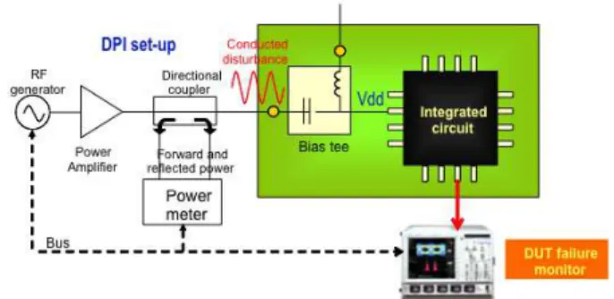
Characterization of components immunity consists, according to IEC 62132-3 [7], in superimposing RF disturbances to a low frequency signal through a decoupling network, to couple
a conducted disturbance to a pin of a circuit (figure 2). The direct power injection (DPI) is an efficient method to couple disturbances to the circuit. Susceptibility is characterized over the band 10 MHz to 1 GHz.
Figure 2. Direct Power Injection test set-up
Once EMC and ageing procedure set-ups have been completely defined, they have to be validated experimentally. A validation step is necessary to ensure that ageing procedure is the only responsible of DUT EMC drifts. The EMC validation step must ensure that the EMC measurements are enough repeatable to extract precise information concerning the EMC drifts related to ageing effects. Measurement repeatability and uncertainties set a limit for the consistence of EMC level drifts. For all experiments, the components should be still functional in nominal condition after aging. At the end of the measurement campaign, the EMC measurement results obtained before and after ageing are processed to extract statistical data concerning the EMC level drifts, such as the worst case and the mean drifts. These data are required to predict the risk that a component becomes incompliant after ageing and, if necessary, readjust the EMC margins at the design level.
Variations of emission or susceptibility levels are given in terms of mean drift ∆M over all the components:
(
)
∑
=−
=
Δ
N 1 i Bi Ai MX
X
N
1
XAi : emission or immunity level of sample ‘i’ after aging
XBi : emission or immunity level of sample ‘i’ before aging
N: number of samples
Emission and susceptibility levels cannot be accurately known as they are subject to statistical distributions due to measurement errors and variability between components. Aging can affect the variability of component characteristics so the dispersion σ of emission or susceptibility levels must be computed before and after aging:
( )
(
)
1
N
X
X
σ
N 1 i 2 B) or (A i B or A−
−
=
∑
=The measured drifts between samples are also affected by repeatability errors owing to the measurement equipment or test bench variations.
III. EXPERIMENTAL RESULTS
A. Initial measurements
In order to exhibit aging effect on IC EMC, the EMR methodology has been applied to a 65 nm low power CMOS technology test chip developed by ST-Microelectronics and dedicated to the characterization of several I/O structures [8]. Standard conducted emission is characterized by measuring the I/O current consumption on ground pin (figure 3). As far as concerned I/O immunity, RFI are injected on I/O power supply pin (figure 5). These two tests are applied on a batch of 10 components, before and after aging. Two separated batches of 5 components have been placed during 408H in a climatic chamber which regulates the temperature respectively at 150°C (HTOL) and -40°C (LTOL) (AECQ100 protocol) combined with high supply voltage (10% higher than the nominal).
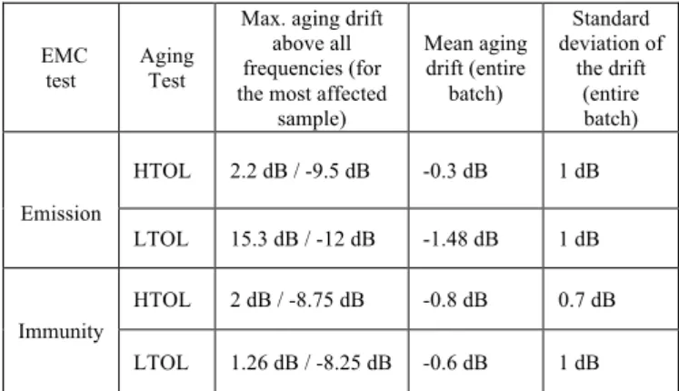
The mean difference (over 5 samples) between the emission levels before and after aging (figure 4) and immunity levels before and after aging (figure 6), for both HTOL and LTOL accelerated life tests have been computed. Experimental results are reported in Table 1.
Emission levels decrease clearly after both aging tests over almost all the frequency range. LTOL induces a greater emission level reduction (with a mean value about -1.48 dB) than high temperature stress (-0.3 dB on average).
Conversely, aging seems to have a negative impact on IO immunity when RF injections are performed on power supply pins. Both aging tests induce a noticeable reduction of the immunity level over a large frequency range. HTOL induces a greater immunity level reduction. Even if the average global fading of immunity level remains acceptable, the large reductions of immunity level observed on some samples at several frequencies (up to -8.75 dB) can seriously affect their EMC compliance.
Weak measurement uncertainties are taken into account. Process dispersion computed characterized before and after stress shows that aging stress doesn’t affect each component on the same way. EMC level dispersion is higher after aging stress than before.
These first experiments that exhibit some potential issues due to EMC levels evolution after aging, clearly indicate that there is a direct link between internal degradation mechanisms and EMC behavior.
Figure 3. HTOL aging impact on emission level (measured on one sample)
Figure 4. LTOL and HTOL aging impact on emission level (mean drift for all samples)
Figure 5. HTOL aging impact on IO immunity threshold (RFI injected on the IO power supply of one sample)
-2,5 -2 -1,5 -1 -0,5 0 0,5 1-10 MHz 10-20 MHz 20-40 MHz 40-70 MHz 70-100 MHz 100-150 MHz IO imm un
ity level mean d
rift af ter aging (d B) HTOL LTOL
Figure 6. LTOL and HTOL aging impact on immunity level (mean drift for all samples) -5 -4 -3 -2 -1 0 1 10-30 M Hz 40-60 M Hz 70-90 M Hz 100 -120 MHz 130 -150 MHz 160 -180 MHz 190 -210 MHz 220 -240 MHz 250 -270 MHz 280 -300 MHz Em iss io n mean d rift a ft er ag in g (d B) HTOL LTOL
This study has been done with the financial support of French National Research Agency (project EMRIC JC09_433714), the regional council of Midi-Pyrénées
EMC test
Aging Test
Max. aging drift above all frequencies (for the most affected
sample) Mean aging drift (entire batch) Standard deviation of the drift (entire batch) Emission HTOL 2.2 dB / -9.5 dB -0.3 dB 1 dB LTOL 15.3 dB / -12 dB -1.48 dB 1 dB Immunity HTOL 2 dB / -8.75 dB -0.8 dB 0.7 dB LTOL 1.26 dB / -8.25 dB -0.6 dB 1 dB Table 1. Summary of LTOL and HTOL aging impact on emission and
immunity levels
B. Impact of semiconductor device parameters drifts
During their lifetime, CMOS transistors are affected by intrinsic failure mechanisms such as time dependent dielectric breakdown (TDDB), negative bias temperature instability (NBTI) or hot carrier injection (HCI), mainly activated by harsh environmental conditions such as high or low temperature and electrical overstress. The failure origins and modelling are studied for years and active researches are still on-going. Among them, HCI and NBTI are the major contributors to the device performance degradation in advanced CMOS technologies. The degree of degradation of a device and, hence, its lifetime depend on the stress level and duration (Table 2). Applying a high level stress (e.g. high temperature or high voltage) for a short period accelerates the damage rate for relevant wear-out failure mechanisms. This principle is commonly used in accelerated-life tests to extrapolate semiconductor device lifetime or in screening tests.
Failure mechanism
Cause of failure Failure modes Stress conditions
Hot carrier injection
(HCI)
Trapped carrier in gate oxide due to
the impact ionization of channel carriers
near the drain region.
Threshold voltage shift and
mobility degradation. Serious issue in short channel NMOS transistor. LTOL High positive voltage VDS Medium positive voltage VGS Negative Bias Temperature Instability (NBTI) Formation of fixed-oxide charge in PMOS gate oxide. Threshold drift with partial recovery phenomenon. Serious issue in thin oxide PMOS
transistor. HTOL High negative voltage VGS Low negative voltage VDS
Table2. CMOS transistor intrinsic failure mechanisms and failure modes
A dedicated test chip has been developed in Freescale CMOS 90 nm technology to characterize the failure mechanisms and the associated MOS transistors electrical parameter drifts. The test chip contains MOS devices with various geometrical and gate options (thin and thick oxide options, with nominal operating voltages equal to 1.2 and 3.3 V respectively). The transistor terminals (gate, drain, source, bulk) are accessed with DC probes. Ids characteristics of transistors have been measured with a Keithley 2601A source meter and an acquisition board after several electrical stress periods. The tests aim at characterizing NBTI in PMOS and HCI in NMOS devices specifically. More details about the measurement set-up and results can be found in [9]. Temperature is not considered in our experiments to simplify the set-up. All the tests are performed at ambient temperature.
The experimental characterizations show that HCI and NBTI effects arise in NMOS and PMOS devices respectively when electrical stresses are applied. Threshold voltages VTH
and saturation currents Idsat are strongly affected depending on
the stress voltage and duration for both transistors. Experimental results on NMOS transistors are given in Table 3. Changes of transistors physical characteristics such as threshold voltage and mobility could affect the emission and susceptibility levels of integrated circuits by modifying electrical behavior of internal functions such as noise margins, Jitters, current consumptions, delays…
Stress conditions ΔIdsat ΔVth After 2000 s @ 3 V - 40 % + 25 % After 500 s @ 4 V - 75 % + 40 %
Table 3: Characterization of HCI impact on thin oxide NMOS transistors
To illustrate the effect of degradation mechanisms on IC EMC behavior figure 7 presents the power supply voltage fluctuations produced by the 90nm digital core activity measured by an on-chip sensor before and after accelerated aging stress (over voltage stress). A -30 % reduction of the peak-to-peak amplitude is observed. The waveform of the signal is also modified. This modification of power supply voltage bounce shape has a direct impact on the component emission spectrum [10].
Figure 7. Evolution of the core power supply voltage bounce after 120 minutes of 3.6 V electrical stress
59 mV
IV. METHODOLGYAPPLIEDTOTHEPREDICTION
OFAPLLELECTROMAGNETICROBUSSTNESS
In this section, we focus on the evolution of the susceptibility of a CMOS phase-Locked-loop (PLL) to EMI coupled on its voltage controlled oscillator (VCO) power supply after accelerated ageing. The developed methodology is applied to model and explain variations of the VCO electrical behavior and consequently the variation of the PLL susceptibility level. The device under test is a test chip developed in the 0.25µm SMARTMOS technology from Freescale semiconductor dedicated to automotive applications.
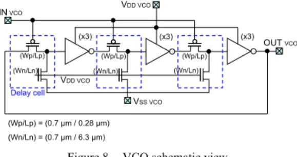
Figure 8. VCO schematic view
The PLL is made of three sub-blocs that have their own separated power supply pins: a phase detector, a VCO and a frequency divider. The VCO is a delay-controlled ring oscillator as shown in figure 8, designed to operate nominally at 112 MHz. The delay introduced by the three delay cells depends on the voltage applied on the gate of their PMOS transistors. The voltage on NMOS gates is constant.
As ICs embedded in automotive applications often suffer from high temperature, High Temperature Operating Life (HTOL) stress is applied. Ten components are tested and placed during 408 h in a climatic chamber which regulates the temperature at 150 °C. An external source provides a power supply 10% higher than the normal supply voltage. DPI tests are conducted before and after aging stress. Susceptibility is characterized over the band 10 MHz to 1 GHz and the maximum forward power is set to 45 dBm. This value, larger than usual maximum power level used in DPI tests (30dBm), has been chosen to induce failure on a large frequency range. Three susceptibility criteria are considered: a static margin of the output amplitude set to 20% of the power supply VDD, a dynamic margin set to
20% of the output signal period (8ns) and a power current limited to 40 times the nominal current.
A significant evolution of the susceptibility for conducted injection on VCO power supply has been observed on the 10 samples of the batch after aging. Immunity level reduction can reach up to 10 dB over a large frequency range on some samples. A statistical analysis shows that among 10 samples after HTOL the maximum reduction is 15.88dB; while the mean reduction for all 10 samples over all frequency is 2.6 dB (figure 9) with a standard deviation 3.64dB. These results indicate that ageing and induced intrinsic degradation mechanisms affect considerably the PLL immunity to power supply ripple.
Figure 9. Evolution of the average susceptibility level measured on a lot of 10 samples before and after accelerated aging test
HTOL mainly accelerates NBTI that can degrade transistor parameters, which could constitute the source of the immunity level variation after ageing. Degradation of transistor transconductance (gm) and mobility (l) could directly affect the power supply rejection ratio and delay time of gates composing the VCO. The prediction of immunity level change induced by aging relies on a model able to simulate the susceptibility level and a physical model that simulates the impact of aging induced degradation mechanisms. To take into account both specifications, a transistor based model is used for the VCO modeling in order to integrate the effect of device aging. The degraded transistors can be identified and their characteristics can be changed according to an aging model.
The structure of the PLL susceptibility model relies on ICIM standard proposal [11]. The model presents two parts:
• The Internal Behavior (IB) block which describes the nominal operation of the PLL and detects failures induced by coupling of EMI
• The Power Distribution Network (PDN) that describes the coupling path of the EMI to the sensitive nodes of the PLL. The PDN includes the DPI system, board tracks, package and on-chip interconnects.
Once PLL Immunity model has been validated, aging model has to be included. A quantitative prediction of the effect of aging on susceptibility relies on the identification of critical transistors and the extraction of variation laws of transistor electrical parameters vs. stress conditions and time. Using CAD simulations, different scenarios of transistor degradation can be tested. In the following analysis, we assume that threshold voltage and mobility are the only model parameters affected by aging. Experimental results have shown that the susceptibility increase is correlated with VCO slowing down so the degradation can be located on the transistors which have a major contribution on VCO oscillation frequency: the delay cell. Degradation mechanisms such as NBTI can increase the channel resistance of the delay cell PMOS transistor and the delay. NBTI applied on the PMOS transistor also decreases the carrier mobility and increase the threshold voltage. The variation of the VCO oscillation frequency is simulated for an arbitrary change on the carrier mobility and threshold voltage values. A change of 10% on a transistor parameter is usually considered as a failure. The worst-case degradation scenario is now considered: the mobility is decreased while the threshold voltage is increased by 10% from their nominal value. The PLL susceptibility level is simulated between 10MHz and VDD VCO (x3) INVCO (x3) (x3) VSS VCO VDD VCO OUT VCO Delay cell (Wp/Lp) (Wp/Lp) (Wp/Lp) (Wn/Ln) (Wn/Ln) (Wn/Ln) (Wp/Lp) = (0.7 µm / 0.28 µm) (Wn/Ln) = (0.7 µm / 6.3 µm)
1GHz. Figure 10 presents the comparison between the simulated susceptibility level of fresh and aged PLL.
Figure 10. Comparison between simulated susceptibility level of fresh and aged PLL
The simulation predicts a global reduction of several dB of the immunity level over a large frequency range (Fig. 10). This trend is similar to the immunity level decrease observed in measurement (Fig. 9). The degradation of the mobility and threshold voltage of the delay cell PMOS transistor is responsible for a large part of the reduction of the PLL robustness to conducted interferences. The proposed model reproduces qualitatively the measured evolution of the susceptibility level of the PLL to conducted disturbances. A better transistor model would certainly improve immunity level drift prediction.
V. CONCLUSION
This paper gives an overview of EMRIC project that aimed at developing a new research activity that mixes electromagnetic compatibility (EMC) and integrated circuits (ICs) reliability. The long-term EMC has to be ensured at circuit design level to guarantee a high level of safety of the final electronic applications. This paper has araised the fact that natural aging in harsh environment condition may affect EMC of electronic systems. The link between ICs internal degradation mechanisms, electrical parameters drifts and EMC evolution has been exhibited. A simulation methodology to predict the impact of circuit aging on conducted susceptibility has been presented. This method has been applied to model and explain the variation of susceptibility level of a phase-locked loop measured after an accelerated-life test. An electrical model of the PLL has been developed to predict the susceptibility level of the PLL to conducted disturbances coupled on the VCO power supply pin. A hypothesis has been proposed about the origin of the susceptibility level drift. The degradation of carrier mobility and threshold voltage of the
PMOS transistor of the VCO delay cell slow down the VCO, modify the capture range of the PLL and thus increase the susceptibility. Including the change of transistor parameters in the susceptibility model has induced a similar reduction of immunity level as the measured one. Although the presented simulation results remain qualitative, the characterization and the accurate modeling of transistor degradation mechanisms will allow a quantitative prediction of susceptibility level drifts.
REFERENCES
[1] Ben Dhia, S., Ramdani, M., Sicard, E., 2005, EMC of Ics: Techniques for low emission and susceptibility, Springer, ISBN 0-387-26600-3 [2] Ramdani, M. Sicard, E. Boyer, A. Ben Dhia, S. Whalen, J.J.
Hubing, T.H. Coenen, M. Wada, O., "The Electromagnetic Compatibility of Integrated Circuits—Past, Present, and Future", IEEE Transactions on Electromagnetic Compatibility, Volume 51, Issue 1, pp 78 - 100, February 2009
[3] M. White, J. B. Bernstein, “Microelectronics Reliability: Physics-of-Failure Based Modeling and Lifetime Evaluation”, NASA WBS 939904.01.11.10, 2008, nepp.nasa.gov.
[4] B. Li, A. Boyer, S. Ben Dhia, C. Lemoine, “Ageing effect on electromagnetic susceptibility of a phase locked loop”, Microelectronic Reliability, Vol. 50, Issues 9-11, September – November 2010, pp. 1304-1308.
[5] I. Montanari, A. Tacchini, M. Maini, “Impact of thermal stress on the characteristics of conducted emissions”, 2008 IEEE Int. Symposium on Electromagnetic Compatibility, EMC 2008, Detroit.
[6] IEC 61967-4, “Integrated Circuits, Measurement of Electromagnetic Emissions, 150 KHz - 1 GHz: Measurement of Conducted Emissions, 1 Ω/150 Ω Method”, IEC standard, 2006.
[7] IEC 62132-3, “Direct RF Power Injection to measure the immunity against conducted RF-disturbances of integrated circuits up to 1 GHz” , IEC standard, 2007.
[8] Ben Dhia, S., Boyer, A., Li, B., Ndoye, Characterization of the Electromagnetic behavior drifts of a nanoscale IC after Accelerated Life Tests”, Electronic Letters, 18th February 2010, Vol. 46, no. 4
[9] N. Berbel, R. Fernandez-Garcia, I. Gil, B. Li, A. Boyer, S. Ben Dhia, “Experimental verification of the usefulness of the nth power law MOSFET model under hot carrier wear out”, Microelectronics Reliability, vol. 51, no 9 -11, pp. 1564-1567, September 2011
[10] A. Boyer, S. Ben Dhia , “ Characterization and Modeling of Electrical Stresses on Digital Integrated Circuits Power Integrity and Conducted Emission ”, 9th International Workshop on electromagnetic Compatibility of Integrated Circuits, EMCCompo 2013, Dec. 15 – 18, 2013, Nara, Japan.
[11] A. Boyer, S. Ben Dhia, C. Lemoine, B. Vrignon, “Construction and Evaluation of the Susceptibility Model of an Integrated Phase-Locked Loop”, 8th International Workshop on electromagnetic Compatibility of Integrated Circuits, November 6 – 9, 2011, Dubrovnik, Croatia.