CMOS Inverse Doping Profile Extraction and
Substrate Current Modeling
by
Eric Pop
Submitted to the Department of Electrical Engineering and Computer Science
in Partial Fulfillment of the Requirements for the Degrees of
Master of Engineering in Electrical Engineering and Computer Science
and
Bachelor of Science in Electrical Science and Engineering
at the
MASSACHUSETTS INSTITUTE OF TECHNOLOGY
JUNE 1999
©
Eric Pop, MCMXCIX. All rights reserved.
The author hereby grants to MIT permission to reproduce and distribute publicly
paper and electronic copies of this thesis document in whole or in part.
A u th or ...
V....
...
...
Department of Electrical Engineering and Computer Science
May 14, 1999
Certified by ...
Dimitri A. Antoniadis
Professor
Thesis Supervisor
I, --z A ccepted by ... ... . A.-.. ... ... -' Arthur C. SmithChairman, Department Committee on Graduate Students
ENG
MAS$*E
JUL
CMOS Inverse Doping Profile Extraction and
Substrate Current Modeling
by Eric Pop
Submitted to the Department of Electrical Engineering and Computer Science on May 14, 1999, in Partial Fulfillment of the Requirements for the Degrees of
Master of Engineering in Electrical Engineering and Computer Science and
Bachelor of Science in Electrical Science and Engineering
Abstract
CMOS substrate current considerations play an important role in modern device design. Powerful, reliable and predictive simulation capabilities are essential to this effort. Such accurate substrate current simulations demand two requirements: knowledge of the E-field distribution, hence of the 2-D device doping profiles, and knowledge of the hot-carrier distribution both in momentum and position space. This thesis investigates the use of inverse doping profile extraction from device capacitance measurements with the help of a non-linear optimization program based on the Levenberg-Marquardt algorithm. It is shown that such a method leads to 2-D doping profiles that can be used for good device capacitance and current simulations. This thesis also implements a simple new impact ionization model based on a parameterized carrier distribution function with a high-energy tail. The new model is implemented in the device simulator FIELDAY and it is calibrated by comparisons of substrate current simulations and data. It is shown that the optimized doping profiles are essential for accurate simulations of the substrate current in MOSFETs.
Thesis Supervisor: Dimitri A. Antoniadis Title: Professor
Acknowledgments
The work presented in this thesis was conducted between June 1998 and January 1999 while I was a co-op within the VI-A program at IBM Microelectronics in Essex Junction, VT. The thesis document itself was written upon my return to MIT in the spring of 1999. As such, there are many people, at both institutions, that have contributed in one way or another and have helped me along the way.
First and foremost I would like to thank Jim Slinkman, my main IBM mentor. A lot of this thesis would not have been possible without his help, patience and guidance. Among other things, he has taught me the intricacies of TCAD device simulations and has provided me with inspiration when I was stuck. I must also thank Prof. Dimitri Antoniadis, my MIT thesis advisor, for agreeing to supervise this project. He has provided me with precise help and guidance while I was away at IBM, and has continued to do so when my thesis work began to crystallize into the final document after my return to MIT.
I must thank Steve Furkay and Jeff Johnson of IBM for many helpful discussions related to device or process simulation, and Bill Clark of IBM for discussions related to device physics. I have learned a lot from them. My IBM manager Peter Cottrell has been a model of efficiency and resourcefulness. Also from IBM, I must thank Robert Gauthier and Don Cook who have helped me obtain all the hardware and the data I needed for my work.
Back at MIT I would like to thank my VI-A advisor, Prof. Steve Senturia who has also served as my academic mentor for the past three years. I must also thank my friend Ken Esler for providing me with the extra storage space on his own Linux workstation when the amount of data I brought back from IBM exceeded my Athena quota.
Finally, I would like to thank IBM for funding my research assistantship during the fall term, and Prof. Jesus del Alamo for taking me on-board as a teaching assistant for 6.012 during the spring semester.
Contents
1 Introduction 15
1.1 E volution . . . . 15
1.2 Today's Problems . . . . 15
1.2.1 Uneven Scaling . . . . 16
1.2.2 Hot Carrier Effects . . . . 16
1.3 TCAD Simulation . . . . 18
1.4 The Scope of This Work . . . . 19
1.5 O rganization . . . . 20
2 Some Existing Doping Profiling Methods 21 2.1 Destructive Methods ... ... 21
2.2 Non-Destructive Methods . . . . 23
3 Inverse Doping Profiling from C-V Measurements 27 3.1 Junction Capacitance . . . . 27
3.1.1 Relationship to Substrate Current . . . . 28
3.1.2 The Inverse Problem . . . . 29
3.1.3 Solving for the Junction Capacitance . . . . 32
3.1.4 Experimental Measurements . . . . 34 3.1.5 Optimization Results . . . . 35 3.2 Gate Capacitance . . . . 37 3.3 Gate-to-Source Capacitance . . . . 39 3.3.1 Capacitance Components . . . . 39 7
8 CONTENTS
3.3.2 Experimental Measurements . . . . 42
3.3.3 The 2-D Problem . . . . 43
3.3.4 The FITDRF Optimizer . . . . 43
3.3.5 Gate Voltage Dependence . . . . 44
3.3.6 Source Voltage Dependence . . . . 49
3.4 Drain Current Simulations . . . . 50
3.5 Sum m ary . . . . 51
4 Substrate Current Modeling 53 4.1 M otivation . . . . 53
4.2 Impact Ionization . . . . 54
4.3 Historical Background . . . . 56
4.4 Device Simulation . . . . 57
4.4.1 The Post-Processed Approach . . . . 58
4.4.2 The Self-Consistent Approach . . . . 60
4.5 Temperature-Dependent Impact Ionization Modeling . . . . 60
4.5.1 The Sch511-Quade Model . . . . 62
4.5.2 The Modified Distribution Function . . . . 64
4.5.3 The Modified Impact Ionization Rate . . . . 65
4.5.4 FIELDAY Implementation . . . . 66
4.6 Substrate Current Simulations . . . . 67
4.7 D iscussion . . . . 69
4.8 Sum m ary . . . . 72
5 Conclusions 75 5.1 Sum m ary . . . . 75
5.2 Discussion and Suggestions for Future Work . . . . 77
A The Levenberg-Marquardt Algorithm 81 B The FITDRF Optimizer 85 B .1 P urpose . . . . 85
CONTENTS
B.2 Usage ... ... 85
B.3 The Input File ... ... 86
B.4 Other Input Files ... . 87
B.5 Program Output ... ... 88
B.6 Timing and Speed Issues . . . . 88
B.7 Other Technical Issues . . . . 89
C Sample Input Files 91 C.1 DOPING Input File . . . . 91
C.2 REGRID Input File . . . . 92
C.3 FIELDAY Input File . . . . 93
C.4 FITDRF Input File . . . . 93
Bibliography
9
List of Figures
1-1 Schematic of impact ionization processes in n-MOSFETs. The circle repre-sents the place where the impact ionization event took place and the new electron-hole pair was created. . . . . 17
3-1 The junction capacitance of a MOSFET . . . . 28 3-2 General schematic of the inverse method used to extract a structure's doping
profile when its C-V characteristics are known. . . . . 31 3-3 Comparison of junction capacitance per unit area measured across 3 different
chips (symbols) and simulation (lines) before and after the doping profile optim ization. . . . . 36 3-4 Vertical junction net active doping |Nd - Na|: initial and extracted profiles.
The left side of the junction is the n+ source and the right side is the p-type
substrate. ... ... 36
3-5 High frequency (HF) and quasi-static (QS) C-V data averaged over seven consecutive measurements in order to reduce experimental noise. The ex-tracted interface trap distribution as a function of gate voltage is shown in the insert. . . . . 38
3-6 The various components that make up the gate-to-source capacitance, Cs. Also marked on the figure are the gate-source overlap L,,, the oxide thickness
t,., and the gate thickness t9. ... .. ... 40
LIST OF FIGURES
3-7 Mesh used in FIELDAY for Cgs simulation. Compare with Figure 3-6 and note the presence of the gate side-wall spacer and the top passivation ox-ide. The mesh has been optimized for device simulation using the program
R E G R ID . . . . 44
3-8 Schematic of the inverse modeling method used to extract the 2-dimensional doping profiles based on Cg, measurements. The dotted line surrounds the three programs that make up the "forward" solver. . . . . 45 3-9 Plot of gate-to-source capacitance data across 3 chips (symbols) and several
simulations (lines) as a function of gate voltage. The solid line represents the simulation with the optimized doping profile and the dotted lines repre-sent simulations done using a lower channel doping and a lower gate length, respectively. . . . . 47 3-10 Plot of gate-to-source capacitance data across 3 chips (symbols) and several
simulations (lines), as a function of gate voltage. The simulations were run with and without the top oxide (passivation) and with and without the gate
side-w all spacer. . . . . 47 3-11 Comparison of gate-to-source capacitance per unit gate width measured across
3 different chips (symbols) and simulation (lines) before and after the doping profile optimization - as a function of source voltage. . . . . 48 3-12 Lateral junction net active doping: initial guess and extracted profile at 0.1
microns below the oxide/silicon interface. The left side of the junction is the n-type source and the right side is the p-doped substrate. . . . . 48 3-13 Measured and simulated drain currents per unit width for devices with 0.5,
0.6, 1.0 and 5.0 microns gate length. The width of the measured devices was 20 microns. The drain bias was set at 5 V whereas the source and the substrate were grounded. . . . . 51 3-14 Log scale comparison between simulated drain currents and data for the same
devices as in Figure 3-13. . . . . 52 12
LIST OF FIGURES
4-1 Schematic representation of the screened electron-electron interaction corre-sponding to impact ionization in an indirect band gap semiconductor (such as silicon). The top parabola represents the conduction band, while the bottom one is the valence band. . . . . 55 4-2 Block diagram of a device modeling scheme, such as the one in FIELDAY II. 61 4-3 Log scale comparison between the simple Maxwellian fsq(k) (solid line) used
in Sch6ll-Quade's model and the new high energy tail distribution function
fhet(k) (dotted line). The comparison is done for T = 300 K and r = 1.8. . 66
4-4 Log scale comparison between the original Sch6ll-Quade impact ionization rate G" (u) (solid line) and the modified high energy tail G"et(u) model (dotted line). The comparison is done for T = 300 K, r = 1.8 and Eth = 1.12 eV (the silicon band gap). . . . . 67 4-5 Measured (symbols) and simulated (lines) substrate currents for the four
devices under investigation - with gate lengths of 0.5, 0.6, 1.0 and 5.0 mi-crons (from top to bottom). The impact ionization parameters used were
ETHN=1.12, TAUNO=1.26E-14 and RHETN=1.32. The drain bias was
V ds = 4 V . . . . 69 4-6 Comparison of measured (symbols) and simulated (lines) substrate currents
for the same devices as in Figure 4-5. Only the high-energy tail parameter was changed to RHETN=1.0, forcing the impact ionization rates to be computed with the old (simple Maxwellian) energy distribution function. . . . . 70 4-7 Another comparison of measured (symbols) and simulated (lines) substrate
currents. The simulations above were obtained from devices with the non-optimized doping profiles used as initial "guesses" in the inverse modeling procedure described in chapter 3. RHETN=1.32 was used . . . . . 71
Chapter 1
Introduction
1.1
Evolution
As the semiconductor industry has progressed over the past thirty years, integrated circuit densities have increased tremendously. In fact, the number of transistors on a chip has been doubling every 18 to 24 months, an observation that has come to be known as "Moore's Law" after Gordon Moore, the man who first noted it. Intel's first processor, the 4004, contained 2,300 transistors whereas today's complex microprocessors incorporate close to 10 million transistors and are up to a quarter million times faster. Unfortunately, such aggressive decrease in device size and increase in circuit density have not been possible without bringing along a variety of limitations.
1.2
Today's Problems
Despite the nearly exponential decrease in integrated circuit feature size over the years, it is apparent that this trend cannot continue going on forever. Both business and real physical limitations are sooner or later likely to slow it down. As chip densities rise, the cost of production goes up almost exponentially. As circuit complexity increases it has become virtually impossible to exhaustively test a computer chip. And as the minimum feature size drops below 0.1 microns - or a couple of hundred atoms across - the atomic and quantum mechanical nature of materials start creeping up and introducing new problems. It is now
Chapter 1. Introduction
generally believed that due to a combination of the limitations described above, "Moore's Law" will significantly slow down in the next 20 years.
1.2.1 Uneven Scaling
Although the size of the transistor has been aggressively scaled down in search for ever higher processor speeds and corporate profit margins, the power supply voltage has often escaped scaling for the sake of compatibility with existing systems and maintaining circuit speed margins. For example, the power supply voltage was kept at 5 V from the mid seventies, when transistors had typical channel lengths of about 5 microns and gate oxides around 1000 A, until the late eighties when the average transistor dimensions had shrunk by about a factor of 5 (see Table 1.1). Some relief came with the introduction of the 3.3 V, and more recently the 2.5 V supplies, but today's sub-micron transistors are still experiencing electric fields that are higher than ever, leading to numerous concerns regarding their reliability and further scaling.
Year
Parameters 1976 1980 1984 1988 1992 1996
Gate Length (pm) 5 3 2 1 0.5 0.35
Gate Oxide (nm) 100 60 40 20 12 8
Supply Voltage (V) 5 5 5 5 3.3 2.5
Table 1.1: Average industry-wide device scaling trends over the last quarter century.
1.2.2 Hot Carrier Effects
It is very common to find transistors with channel lengths under 0.5 microns and gate oxides below 100 A operated under 3.3 or even 5 V power supplies in modern integrated circuits. Moreover, some technologies that are designed to operate at 3.3 V need to be modified to accommodate 5 V devices on their chips (e.g. for I/O purposes). This com-bination of high voltage and small dimensions leads to very high electric fields that can reach more than 100 kV/cm during the normal operation of a transistor. The high electric
1.2. Today's Problems
Gate
Source
Drain
e-Substrate
h+
Figure 1-1: Schematic of impact ionization processes in n-MOSFETs. The circle represents the place where the impact ionization event took place and the new electron-hole pair was created.
fields in turn accelerate the mobile charge carriers to very high velocities, leading to what are known as "hot-carrier" effects. When these highly energetic carriers travel through a semiconductor there are two main phenomena that can occur. First, a carrier may ac-quire enough energy to break a lattice bond in the semiconductor. This phenomenon, also known as impact ionization, has been recognized and studied from the earliest days of the semiconductor industry [1, 2]. In the case of an n-MOSFET, the hole of the generated electron-hole pair travels towards the substrate contact, where it is collected in the form of the substrate current
[3).
The impact ionizing electron and the generated electron are both usually collected by the device drain, as illustrated in Figure 1-1. Hot carrier phenomena are less of a concern in p-MOSFETs because the channel carriers' mobility and impact ionization rates are typically several times lower than in similar n-MOSFETs. The typical p-channel device substrate current is about three orders of magnitude lower than that of an n-channel device [4], and thus substrate current studies (including this one) generally focus on n-MOSFET issues.Secondly, the channel carriers (or even the secondary generated carriers) may be scat-tered towards the silicon/insulator interface after a collision in which their momentum 17
Chapter 1. Introduction
changes direction by just the right amount. If their energy is large enough, these "lucky" carriers [5] can create interface states, or fill interface or bulk traps - either of which can lead to the accumulation of fixed charge at the silicon/insulator interface and ultimately to the degradation of the device. Moreover, some of these carriers may have enough energy to get injected directly into the conduction band of the insulator and then drift to the gate where they are collected as gate current. Therefore, due to their origin, both the substrate and the gate current have been used to monitor the hot-carrier, device-degrading effects taking place in modern MOSFETs.
High substrate currents by themselves can be damaging as well, as they can lead to overload of the circuit substrate-bias generator and can induce snap-back breakdown and CMOS latch-up [6, 7]. Hot carriers are also responsible for the photo-current that can degrade DRAM refresh times, whose origin is found in the bremsstrahlung radiation [8] emitted when an energetic carrier is decelerated by an impurity ion.
1.3
TCAD Simulation
Given the impact that hot carrier effects have on modern device reliability, it has become very important that they be modeled accurately and consistently. In fact, with the increase in our available computational power, Technology Computer-Aided Design (TCAD) sim-ulations have become an essential part of the design of new generations of semiconductor devices [9]. Accurate, predictive simulations can save millions of dollars (and months of production time) that would have otherwise been spent testing wafers with countless pro-cess variations. New technologies and devices are much more easily tested in a "virtual fab", and essential design considerations can thus be made long before wafers need to be sent for testing in the real fab.
As devices are shrunk to sub-micrometer sizes, subtle details of the 2-dimensional (2-D) and 3-dimensional (3-D) redistribution of dopants, due to thermal diffusion during the fabri-cation process, strongly determine the device short-channel effects. It is these effects which ultimately limit device operation and performance. For the sake of accurate simulations it has thus become very important to understand what the exact doping profiles of a
1.4. The Scope of This Work
ern device are. Such full-scale simulation is a two-part problem: process simulation [10], which leads to the formation of the device and its physical properties (gate length, oxide thickness, 2-D doping profiles) and device simulation [11], the actual I-V or C-V electrical calculations. Device simulators need (and rely on) accurate process models for their good operation. Therefore accurate device doping profile information, if possible as a function of more than one space coordinate, is an important prerequisite for accurate device simulation.
Unfortunately, much is still unknown about the diffusion of impurities in silicon. Al-though complex computer models such as the process simulator SUPREM [10] exist, there are no measurements that can be performed to directly and accurately determine the 3-dimensional spread of impurities across a device's volume. Such experimental doping profile extraction methods, if available, could be used to:
" provide a check on the fabrication process " serve as input for device simulators
" increase our understanding of dopant atom redistribution in semiconductors, thus also enabling the verification of process simulator models
" help minimize the amount of expensive test hardware used in technology development.
1.4
The Scope of This Work
The first goal of this thesis is to demonstrate the use of inverse 1- and 2-dimensional doping profile extraction both as a process simulator check and as a reliable input for device simu-lator calibration. Simulation results that are particularly sensitive to the doping profile dis-tribution especially benefit from such an approach. In this thesis, doping profile extraction is treated as an inverse problem, whose outputs (e.g. electrical capacitance measurements) are known, but whose inputs (the device-specific doping profiles) are to be found.
The second goal of this thesis is to introduce a new parameterized impact ionization model and to calibrate it through substrate current simulations. The impact ionization model is based on a simple, yet physically-based high-energy-tail correction to the carrier distribution function and is shown to be easily implemented in an existing device simulator. 19
Chapter 1. Introduction
Moreover, it is demonstrated that the substrate current simulations are particularly sensitive to the device doping distribution. Therefore the previously inverse modeled doping profiles are shown to be essential for the accurate calibration of any such new transport models.
1.5
Organization
Chapter 2 of this thesis reviews some of existing doping profile extraction methods and discusses their individual strengths and weaknesses.
Chapter 3 formulates 1- and 2-dimensional doping profiling as an inverse problem whose starting points are the device C-V characteristics. The chosen C-V measurements are discussed and the implementation of the extraction technique is explained. The results are analyzed, and their reliability is assessed. The validity of the extracted MOSFET doping profiles is further supported by good agreement between both C-V and I-V simulations and data.
Chapter 4 begins by describing several approaches that have been taken to model impact ionization in semiconductors. The theory and assumptions behind a particular temperature dependent model [12] are then explored in more depth. A parameterized high energy tail is introduced in the carrier distribution function and the impact ionization rate is re-derived and implemented in an existing device simulator, FIELDAY [11]. The new impact ionization model is calibrated within the context of the previously determined device doping profiles. Chapter 5 provides an overall conclusion of this thesis. The results are analyzed and several pointers are offered for future work.
The three appendices contain, in order, a summary of the least-squares Levenberg-Marquardt algorithm, a thorough description of the inverse modeling and parameter ex-traction program written for the purposes of this thesis, and several examples of simulator input files. The work described in the following four chapters and three appendices should provide enough detail to enable anyone with similar resources to duplicate the results of this thesis.
Chapter 2
Some Existing Doping Profiling
Methods
This chapter reviews some existing doping profile extraction methods and discusses their individual strengths and weaknesses. All existing doping profile extraction methods can be classified in two broad categories: destructive, such as SIMS, RBS, spreading resistance and AFM, or non-destructive, such as 1- or 2-dimensional capacitance-voltage methods and sub-threshold current-voltage methods.
2.1
Destructive Methods
The main characteristic (and disadvantage) of destructive doping profiling methods, as their name suggests, is that the semiconductor wafer is at least partly destroyed in the process. Application of destructive methods to process monitoring is therefore undesirable. In destructive methods, usually thin layers of semiconductor material are removed from the
surface of the device (or special test structure). Next, either the contents of the removed layer is analyzed or the behavior of the remaining device is measured. Layers may be removed by sputter etching with an ion beam, by beveling or by anodic oxidation followed by a selective wet etch to remove the oxide layer.
Secondary Ion Mass Spectroscopy (SIMS) uses an ion beam (e.g. Cs+ at 10 keV) to continuously remove layers from the top of the semiconductor surface [13]. The ionized
Chapter 2. Some Existing Doping Profiling Methods
particle stream eroded from the sample is analyzed by a mass spectrometer. If the erosion speed is known, the evolution of each species as a function of time can be used to find its distribution as a function of depth into the sample. SIMS analysis usually requires large test structures and the obtained data is not very reliable near an interface. Also, this technique only measures the total chemical concentration of dopants, not the concentration of ionized dopants - although it is the latter that is mainly responsible for a device's electrical properties. SIMS is by nature a 1-dimensional doping extraction technique, and perhaps the most commonly used one, despite its requirement for expensive equipment.
Rutherford Backscattering Spectroscopy (RBS) uses a 1 -3 MeV 4He+ ion beam to pene-trate the semiconductor surface [131. The incident ions are detected after they are backscat-tered at various energies by elastic collisions with the different atomic species present in the semiconductor sample. A depth profile can be obtained by monitoring the number of backscattered ions as a function of their energy. Unlike for SIMS, no calibration with stan-dards is required to obtain accurate quantitative results, but this technique isn't as sensitive at lower doping levels.
In spreading resistance profiling (SRP) the sheet resistance ps of a sufficiently large area of a semiconductor layer is measured. To obtain a depth profile, a large number of thin, uniform layers are removed [14]. For silicon, this is usually done by anodic oxidation of the surface, followed by a wet etch of the oxide layer. Alternatively, a depth profile can also be obtained by beveling the semiconductor surface at a small angle and probing down the bevel. Spreading resistance techniques are mostly of historical importance, but they still offer some perspective in the profiling of highly doped layers since they are less expensive
than SIMS.
Atomic Force Microscopy (or AFM) is probably the newest among all destructive doping profile measurement methods. It also requires relatively expensive equipment and extensive sample preparation, but it can be used to directly explore cross-sections of actual MOS devices. The technique, also known as Scanning Capacitance Microscopy (or SCM), requires the use of an AFM machine to position a tiny conducting tip over the semiconductor surface. As the tip is scanned across the surface, the change in capacitance measured by the tip is held constant by varying the amplitude of the bias applied to the sample with
2.2. Non-Destructive Methods
a feedback control. This leads to large bias voltages in heavily doped regions and small biases in lightly doped regions. The amplitude of the bias voltage can then be related to the dopant density through a conversion algorithm based on a quasi-3-D model of the tip sample capacitor. Using this method relatively good resolutions of vertical dopant profiles have been recently reported, in good agreement with SIMS measurements [15]. Although some advances towards the achievement of quantitative 2-dimensional doping profiles have also been recently made [161, the results are highly dependent on the quality of the probe tip and of the surface preparation. The AFM/SCM technique is still in its infancy, but it may hold great potential for the future. Nevertheless, the color map profiles that can be obtained today can still be used to at least qualitatively gauge the relative distribution of dopants across the 2-dimensional cross-section of a semiconductor device.
2.2
Non-Destructive Methods
Non-destructive doping profile extraction methods generally use radiation or electrical data to obtain the necessary information. Radiative methods are not too accurate, and can only be used to obtain approximate doping profiles. Their doping sensitivity is not very high, and they are also limited by the maximum penetration depth of the radiation type used. Electrical methods on the other hand are quite popular for a variety of reasons:
" they are non-destructive, and thus useful for on-line process monitoring with standard measurement equipment
" measurements can be directly obtained from the devices whose doping profile must be determined, or from test structures manufactured in the same fabrication process " their experimental acquisition is straightforward
* they are most closely related to the final goal of the doping profile determination: the understanding of electrical device behavior.
The capacitance-voltage (C-V) method for 1-dimensional doping profiling was first men-tioned by Schottky in the 1940's. The early application of the method to Ge diode profiling was reported in the 1960's [17] and many derived methods, too numerous to cite, have since 23
Chapter 2. Some Existing Doping Profiling Methods
been described. The C-V method uses the small signal capacitance of the depletion layer as its starting point. As the reverse-bias voltage across the p-n or MOS structure is varied, the measured capacitance changes due to changes in the depletion layer width. The depletion layer width is also influenced by the spatial variation of the doping profile. In the simplest case, the doping profile can be calculated analytically if it is assumed flat on both sides of the p-n junction. A more realistic scenario however must assume that the doping profile is not flat. A computer program is then needed to determine the depth-dependent 1-D doping profile by searching for doping values whose simulated C-V characteristics match the experimental ones.
With the increase in available computational power, there have been several attempts to implement 2-dimensional inverse doping profile extraction techniques in recent years. The first comprehensive review of various such methods including their reliability and error analysis was first given by Ouwerling [18]. His investigations were however limited to spe-cially designed test structures, more relevant to CCD cells than to transistor devices. More recently, Khalil and Faricelli have demonstrated the use of similar techniques by extracting doping profiles from regular transistor-related test structures, such as fingered overlap ca-pacitors [19]. They used cubic splines to model the 2-dimensional doping profiles and they extracted the splines' parameters with the help of a nonlinear least-squares solver. Their extracted doping profiles were shown to yield good C-V agreement with data for a variety of bias voltages.
Another inverse modeling doping profile extraction method based on electrical measure-ments was recently described by Lee et al. [20, 21]. Their method extracts the 2-D doping profile of sub-micron MOS transistors by using I-V characteristics in the sub-threshold re-gion. They rely on the fact that short-channel effects such as drain-induced barrier lowering (DIBL), sub-threshold slope and punch-through are strongly (exponentially) dependent on the 2-D device doping profiles, and only linearly dependent on other factors such as mobility or gate width. Therefore a relatively accurate doping profile extraction could be performed with the help of a nonlinear least-squares solver, while the uncertainties of the employed mobility model were shown to have only a marginal impact. It is currently believed that such sub-threshold I-V methods are typically more useful when extracting the channel
2.2. Non-Destructive Methods
cluding halo) doping profiles, while the C-V methods are more reliable when describing the source/drain regions of a device. It should also be noted that both the C-V and the I-V methods provide only indirect measures of the device doping. Unlike destructive methods such as SIMS, the C-V or I-V methods measure only the electrically active dopant con-centration, without distinguishing between dopant species of the same type. For example, arsenic and phosphorus produce the same C-V and I-V "signatures" because they are both n-type dopants and they are virtually equivalent from an electrostatic point of view as far as their influence on the electrical device characteristics is concerned. This however is suf-ficient for accurate device simulation, for the exact same reason - because it is only the type and the active doping levels of a device that determine its electrical characteristics.
The next chapter describes the inverse modeling work done in this thesis. The current work is similar to [19], but it uses Gaussian functions (as opposed to cubic splines) to model the doping profiles. Two different gate-to-source capacitance measurements are used in con-junction to extract the 2-dimensional source-drain doping profiles. This work also combines the extraction of most necessary parameters from various experimental measurements and thus makes minimal use of a process simulator. In the end, the validity of the extracted doping profiles is further supported by good agreement between both C-V and I-V simula-tions and data. Like in the work of Lee [20], it is shown that the extracted doping profiles can be used to calibrate device I-V models. In this work the calibration is taken one step further and the extracted doping profiles are used to adjust a new substrate current model. 25
Chapter 3
Inverse Doping Profiling from
C-V Measurements
This chapter is dedicated to formulating 1- and 2-dimensional doping profiling as an inverse problem whose starting points are the device C-V characteristics. The chosen C-V measure-ments are discussed and the implementation of the extraction technique is explained. The results are analyzed, and their reliability is assessed. The validity of the extracted doping profiles is further supported by good agreement between I-V simulations and data.
The doping profiling work done in this thesis specifically relied on depletion capacitance measurements. Several measurements were made, such as junction capacitance (Cj), gate capacitance (C) and gate-to-source capacitance (Cgs). The junction and gate capacitance measurements were used to determine 1-D aspects of the device doping profiles, such as the vertical junction 1-D profile, the junction depth, oxide thickness and oxide charges. The gate-to-source capacitance measurements were used to provide insight into the lateral and 2-dimensional distribution of dopants in the source (and drain) region of the device.
3.1
Junction Capacitance
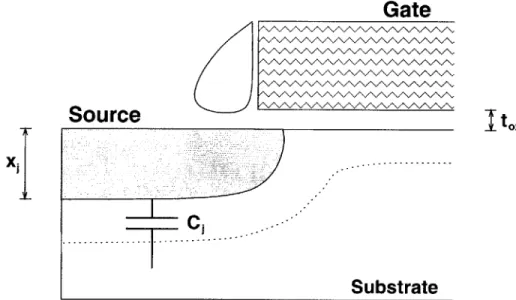
The junction capacitance between the source (or drain) of a MOSFET and its substrate is an important device parameter. It holds clues to the operation speed of the MOSFET, its junction depth, and it can also be used to learn more about the nature of the vertical
Chapter 3. Inverse Doping Profiling from C-V Measurements
Gate
Source
tox
C
Substrate
Figure 3-1: The junction capacitance (Cj) of a MOSFET. The oxide thickness (tox) and metallurgical junction depth (xz) are marked on the figure as well. The dotted line rep-resents the edge of the depletion region into the substrate. The drawing shows half of a typical MOSFET device, including the gate, source, spacer and substrate.
doping profile in this particular region (see Figure 3-1).
3.1.1 Relationship to Substrate Current
It is important to keep in mind that one of the final goals of this thesis is the calibration of a substrate current model. The MOSFET substrate current is usually represented as an exponential function of the maximum electric field (Emax) in most simple first order
models [221:
Isb = aId exp (-F ) (3.1)
where Id is the drain current and a and
#
are parameters. The maximum electric field occurs in the channel, near the drain, and can be expressed as:Vds - Vdsat
Emax = (3.2)
where 1 should be thought of as an effective ionization length and has been shown to be 28
3.1. Junction Capacitance
directly dependent on the source/drain junction depth x [23]:
1 = 0.22 t1/3,i 2. (3.3)
The equation above was empirically determined for long channel and thick oxide devices, but a similar relationship exists for short channel devices [24]. Hence, even in a simple model the substrate current is shown to be directly dependent, to first order, on the MOS-FET source (and drain) junction depth. More complex, 2-dimensional substrate current models must have good information not only about the junction depth, but also about the vertical variation of the source (and drain) doping profiles in order to correctly reproduce experimental results. The doping information provided by the inverse method presented in this chapter is therefore very valuable to the substrate current model calibration described in chapter 4.
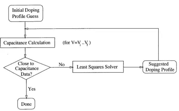
3.1.2 The Inverse Problem
Small signal capacitance measurements with the junction in reverse bias show that Cj is a function of the applied voltage: as the reverse bias across the junction grows, the depletion region widens and the carriers on either side of the junction are pushed apart. This leads to a decrease in C as the voltage (V > 0) applied to the n-type source diffusion increases It has been shown [25] that even for an arbitrary doping profile, the measured junction capacitance per unit area is always inversely proportional to the depletion region width:
C = *S2 (3.4)
Wdep
where esi is the silicon dielectric constant. For the case of a simple 1-dimensional step junction with uniform donor (Nd) and acceptor (Na) profiles, the capacitance has a simple
'The described junction capacitance measurements, as well as the rest of this thesis focus on n-channel MOSFETs. The reason for this focus is ultimately due to the fact that n-channel devices exhibit substrate currents that are about three orders of magnitude higher than those present in p-channel devices. Thus, any other devices described in this work should be implicitly considered to have an n-type channel, source, drain and gate and p-type substrate.
Chapter 3. Inverse Doping Profiling from C-V Measurements
analytical dependence on the applied bias across it [22]:
- EsiqNdNa
2(Nd + Na)(Obi + V) (3.5)
where q is the magnitude of the electron charge and
#bi
is the junction built-in potential. Unfortunately in practice the dopants on either side of the junction are rarely uniform: rather they are strongly varying functions of at least one spatial coordinate (depth). In the general case, the capacitance also depends on this spatial variation of the doping, since the depletion region will be less likely to widen into the higher doped regions. By consequence, this property of the voltage- and dopant-dependent capacitance can be used to extract the spatial distribution of the doping across the p-n junction. The doping profile generally does not exhibit any discontinuities and therefore it can usually be modeled by a parameterized analytical function, likef
(Pi, P2,.--, Pm; x) (3.6)where (Pi ,P2, .. ,Pm) are parameters and x is the spatial coordinate for the 1-dimensional junction capacitance problem. The parameters can then be extracted with the help of a computer program that will search for the set {pi
I
i = 1..m} whose doping profile yields simulated C-V curves that best match the experimental results.In essence, the technique described above is the definition of inverse modeling. The problem is treated as a "black box" whose outputs (experimental C-V curves) are known but whose inputs (the doping distributions) must be found. In practice, the computer program most often enlisted for help in the search for appropriate doping coefficients is a Levenberg-Marquardt nonlinear least-squares solver [19, 26].
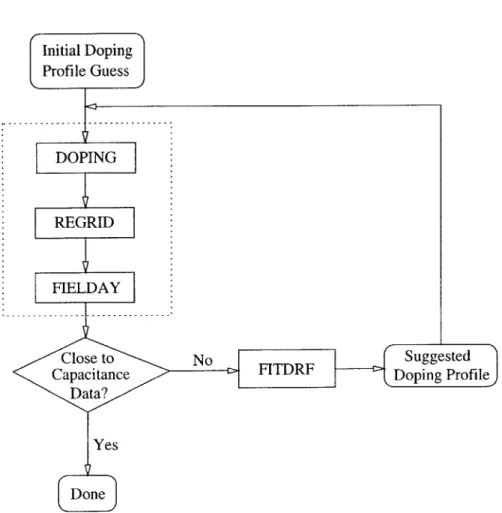
In order to solve the inverse problem an initial guess of the doping profile is first needed. The initial guess may be provided by SIMS analysis, by a process simulator run (e.g. SUPREM) or by using the known doping profiles previously determined for another (sim-ilar) technology. In this work, the latter two options were preferred, since using SIMS to provide the initial guess would undermine the non-destructive property of the C-V method! The general flow of the inverse profiling method is depicted in Figure 3-2. Once the initial guess is provided, a program (the "forward solver") is needed to simulate the first
3.1. Junction Capacitance
(for V=V ..V)
Figure 3-2: General schematic of the inverse method used to extract a structure's doping profile when its C-V characteristics are known.
expected C-V curve. The forward solver can be any program that takes in a set of doping profiles and other device parameters and outputs the computed C-V curve. In other words, it can be a full-blown device simulator (e.g. FIELDAY [11] or MEDICI [27]) or it can be a simple and fast Poisson solver specifically tailored to solve this particular problem. The inverse method treats the forward solver as a black box and does not require any knowledge about its internal workings. The only reason to choose one forward solver over another has to do with its sheer speed and convergence properties. Since the forward problem must be solved many times during the execution of the inverse extraction method, it is important to pick a fast and stable forward solver.
Once the simulated C-V curve is available, the result is compared with the experimental C-V data points. If the mean of the squared differences between the two data sets is deemed too large (by comparison with some user-specified value) the least-squares solver is invoked to find a better set of doping profile parameters. Although not shown on the schematic diagram in Figure 3-2, the least-squares solver in turn reruns the forward problem once 31
Chapter 3. Inverse Doping Profiling from C-V Measurements
more for each parameter pi, with slightly different values pi + 6pi. This way, numerical derivatives of the capacitance with respect to each parameter (&C/&pi) are calculated and the sensitivity of the problem to variations in each parameter is gauged.
When the least-squares optimizer finds a new set of parameters, the forward problem is again rerun, the new simulated C-V curve is compared with the data - and if the difference is still deemed too large the procedure briefly described above is repeated. The problem exits only when a suitable new set of parameters is converged upon. What "suitable" really means, as well as a more detailed discussion of the least-squares optimization procedure is provided in appendix A.
3.1.3 Solving for the Junction Capacitance
In the present work, a forward solver for the procedure described above was to be chosen between FIELDAY or a simpler, specially designed Poisson solver. After some experimen-tation it was decided that a simple program written specifically for the task of solving the 1-dimensional C-V problem was enough, and in fact faster than FIELDAY. After the least-squares-based optimizer was written in C, there was enough code infrastructure that building a fast 1-D Poisson solver and integrating it with the existing code did not present major problems. The entire forward problem is based on an iterative numerical solution of Poisson's equation using Newton's method on a fine enough grid:
V
20(X)-_ __ q [p(x) - n(x) + Nd(x) - Na(x)] (3.7) Esi Esi
where
#
is the potential and n and p are the electron and hole concentrations, respectively. The donor and acceptor doping profiles (Nd and Na) can be expressed with the help of parameterized analytical functions as in equation 3.6. In this work, the analytical functions used to describe the doping profiles are sums of Gaussians, e.g. for Nd:~~m-2
p
xp
(X
-Pi±1)2l(.8Nd(pi, ... , pm; x) = piep 2pi+1 (3.8) 2i+2 .
2=2+3 32
3.1. Junction Capacitance
where pi are parameters whose total number, m, must be a multiple of 3, and x is the spatial coordinate of the 1-dimensional junction. Gaussians were chosen because they are the doping profile shape predicted by the simplest theory of ion implantation in semicon-ductors
[28].
However, due to various heat treatments of a wafer after ion implantation, a single Gaussian may not be enough to describe the final ion distribution. Since three Gaussians would bring too many parameters into the problem, it was decided to choose a reasonable compromise and represent most doping profiles in this thesis as sums of two Gaussians per implant dose.The electron and hole concentrations in Poisson's equation (3.7) can be obtained from Maxwell-Boltzmann statistics written with respect to the carrier quasi-Fermi levels. Heavy doping effects are accounted for by using an effective intrinsic concentration (nieff) as first suggested by Slotboom [29]:
q(#$(x) - (3.9
n(x) = nieff exp kT (3.9)
p(x) = nieff exp -Tp (x)) (3.10)
kT
where the quasi-Fermi levels
#n
and#,
are determined by the voltages applied to the device's terminals, and nieff is Slotboom's empirically determined function of doping and temperature. Since the net charge density is given byp(x) = q [p(x) - n(x) + Nd(x) - Na(x)] (3.11)
the total charge associated with the device terminals can be calculated by integrating
Q = p(x)dx. (3.12)
Although most experimental measurement setups use small-signal (e.g. 50 mV) sinusoidal test voltages, for the purposes of this simulation the capacitance computed in the electro-static approximation
_ dQ Q(V + 6V) - Q(V) (3.13)
C (V)=dv V
Chapter 3. Inverse Doping Profiling from C-V Measurements
is valid and can be used.
3.1.4 Experimental Measurements
The devices studied in this thesis were part of a 3.3 V technology that had been modified to run at 5 V. This was necessary because the core circuitry ran at 3.3 V, but the devices which communicated with the outside world needed to run at 5 V. Since both types of devices had to be built on the same wafer, a few extra process steps were taken to "convert" some of the devices to run out of 5 V power supplies. For example, the 5 V devices were given a thicker, dual oxide layer (roughly 120 A thick) as opposed to the single oxide layer used for the 3.3 V devices (roughly 70 A). The high-voltage devices also had larger minimum channel lengths (0.55 pm versus 0.35 pm) and a different channel implant dose to insure a higher threshold voltage.
Hot carrier effects were diminished by adding an extra source/drain extension implant, in the form of an LDD (Lightly Doped Drain) displaced from the regular high-dose implant by the presence of a spacer. Nevertheless, these devices' measured substrate currents were still relatively high, despite the less steeply graded source/drain junction profiles. The combination of high substrate currents (to be measured), graded doping profiles (to be determined) and a relatively thick oxide (rendering quantum mechanical surface effects somewhat negligible) made these devices a good choice for the study in this thesis.
The junction capacitance C-V data was taken on roughly rectangular, large area and minimum perimeter STI-bound diffusion capacitors. The use of large area capacitors
(75,435 mti2
) is useful because the measured capacitances are proportionally larger and the error due to instrumental accuracy and line noise is minimized. Using large area and minimum perimeter structures also minimizes the error due to the side-wall component of the measured capacitance, and the emphasis is kept on the junction capacitance component. To minimize other parasitic capacitance effects, the setup was calibrated by taking readings with the probes lifted off the wafer and subtracting those values from the actual junction capacitance measurements. To get a sense of the general validity of the acquired data, three different chips were measured on the same wafer, and the C-V measurements were repeated several times and averaged for the diffusion capacitor on each chip.
3.1. Junction Capacitance
3.1.5
Optimization Results
The measured devices' n-type source and drain were formed with a regular high-dose implant and an LDD implant (both being phosphorus), while their substrate was made up of two boron implants (a shallow and a deep one) and the relatively constant background doping
(about 5 x 1015 cm-3).
Using two Gaussian functions for each implant dose (with three parameters for each Gaussian) quickly leads to a total of twenty-four coefficients to be optimized for the entire problem. Such a problem is clearly something best left for a computer to solve. However due to large computation time demands and the possibility of doping coefficients' divergence beyond physically reasonable limits only two or three parameters were optimized at a time, the others being held constant.
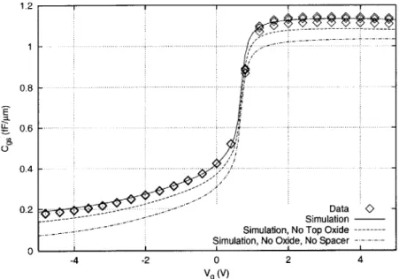
The initial guess was provided by fitting sums of Gaussians to the n- and p-type dop-ing profiles extracted from a SUPREM run. Both intuitively and after a few simulation runs it became apparent that the parameters determining the Gaussians' displacement and standard deviation (e.g. Pi+1 and Pi+2 respectively in equation 3.8) were most strongly responsible for the shape of the C-V curve. Those parameters were allowed to adjust first, other ones being held constant. Afterwards the parameters determining the peak donor and acceptor concentrations were allowed to adjust. In general however, it was found that degenerate peak concentrations (above 1019 cm-3) had little to no effect on the outcome of the C-V curve.
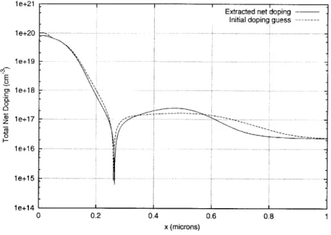
The final results of these computations are displayed in Figures 3-3 and 3-4. The ex-perimental data in Figure 3-3 came from three diffusion capacitors (across three chips) on the same wafer, and several measurements were performed and averaged on each chip. The
doping profile shown in Figure 3-4 was optimized using the average of the C-V data over the three chips. The origin of the x axis in Figure 3-4 is at the surface of the wafer and the extracted junction depth is thus approximately 0.265 pm, in very good agreement with that extracted by SIMS analysis on the same devices at a later point in time.
Despite the good agreement between the final simulated C-V curve and the data, the limitations of the extracted doping profile must be understood. As mentioned before, the extraction method loses its sensitivity for degenerate doping levels (above 1019 cm-3) be-35
Chapter 3. Inverse Doping Profiling from C-V Measurements E 0~ 0.9 0.8 0.7 0.6 - -0 .5 - - --- -0.4 0 1 2 3 4 5 Vs (V)
Figure 3-3: Comparison of junction capacitance per unit area measured across 3 different chips (symbols) and simulation (lines) before and after the doping profile optimization.
E 0 0 0 1e+21 1e+20 le+19 1e+18 1e+17 1 e+16 1e+15 le+14 ' 0 0.2 0.4 0.6 0.8 x (microns) Figure 3-4: Vertical junction net
The left side of the junction is the
active doping |Nd - NaI: initial and extracted profiles. n+ source and the right side is the p-type substrate. 36
3.2. Gate Capacitance
cause the potential variation diminishes there. Also, since this sort of C-V inverse modeling relies on the voltage dependence of the depletion width, the extracted doping profiles are limited by the applied range of voltages. The applied range of voltages is in turn limited by the turn-on of the p-n junction at one end and by junction breakdown at the other. At the maximum applied voltage of 5 V, the maximum width of the depletion region is on the order of 0.3 pm, so the doping profile deeper into the substrate (e.g. for x > 0.6 pm) is susceptible to some error. However the doping profile at such depths has little influence on the general device characteristics. Also it should be noted that very fine details of the doping profile within the depletion region are likely to be averaged out, since the potential in Poisson's equation is a very smooth function in space (being a double integral of the space charge). This may not be a tremendous issue however, since in the processing of MOSFETs the diffusion of dopants also results in smooth doping profiles [203.
3.2
Gate Capacitance
Several gate capacitance measurements were performed in order to determine such device characteristics as the oxide thickness, the polysilicon gate doping and the density of interface traps (DIT) at the Si/SiO2 interface. Like the junction capacitance, the gate capacitance was also measured on specially designed large area (65,457 pm2 ) and minimum perimeter test structures in order to minimize 2-D fringing field effects and the contribution of the side-wall capacitance. The structures used to measure the gate capacitance were rectangular STI-bound capacitors - essentially just large MOS sandwiches with a 0.2 Pm thick phosphorus doped polysilicon gate on top, the p-type silicon substrate underneath, and the dual, thicker oxide in between (corresponding to the 5 V devices). The gate capacitance structures were formed through the same process steps and on the same wafer as the junction capacitance structures previously described, and as the MOSFET devices to be later measured for their I-V characteristics.
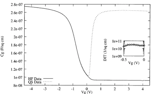
In order to extract the DIT, the method described in [30] was followed: a high frequency (100 kHz) C-V measurement was first performed, followed by a quasi-static sweep with a slow voltage ramp (50 mV/sec). The interface traps can be easily filled or emptied during 37
Chapter 3. Inverse Doping Profiling from C-V Measurements 2.8e-07 I I I 2.6e-07 2.4e-07 2.2e-07 2e-07 U E le+11 1.8e-07 -C000 +> . le+10 1.6e-07 - -le+09 1.4e-07 - -0.5 0 1.2e07 -le-07 ~ HF Data 8e-08 WDt -4 -3 -2 -1 0 1 2 3 4 Vg (V)
Figure 3-5: High frequency (HF) and quasi-static (QS) C-V data averaged over seven consecutive measurements in order to reduce experimental noise. The extracted interface trap distribution as a function of gate voltage is shown in the insert.
the quasi-static measurement, but they cannot keep up with the high frequency signal. Therefore a comparison of the two obtained C-V curves (see Figure 3-5), especially in the
depletion region, can be used to gauge the DIT and its variation with the gate voltage. The
oxide thickness can be computed by linearly extrapolating the high frequency C versus 1/V data in the strong accumulation region, yielding approximately 120 A; the oxide capacitance Co, follows immediately. Quantum mechanical surface effects are nearly negligible in devices with such a thick oxide.
The interface trap contribution to the gate capacitance can be obtained directly from the measured C-V curves, as described in [30]:
Cit (1/CQS - 1|Cox)-1 - (1|CHF - 1/Cox>1 (3.14)
q q
The results of the C-V measurements and the DIT extraction are shown in Figure 3-5. In addition, the polysilicon doping can be inferred by comparing C-V simulations with the acquired data at high gate voltages in the inversion region - where signs of polysilicon
3.3. Gate-to-Source Capacitance
depletion become apparent. Such comparisons indicated that the active polysilicon doping for the MOS structures being tested was around 6.7 x 1019 cm-3. This value was later con-firmed by a similar result obtained from 2-dimensional gate-to-source inversion capacitance measurements (see section 3.3.6).
3.3
Gate-to-Source Capacitance
The two capacitance measurements described thus far have only offered insight into the 1-dimensional (vertical) structure of the devices under study. On the other hand, the gate-to-source (or gate-to-drain) capacitance is essentially a 2-dimensional capacitance, and it can therefore offer insight into the 2-D structure of the MOSFET device.
The gate-to-source capacitance is a key parameter for device reliability and circuit speed. Moreover, its magnitude holds important clues about the lateral extent of the source dif-fusion under the gate. It has been shown [19, 31, 32] that the voltage dependence of the gate-to-source capacitance (Cgs) can be used to probe the extent of the source diffusion under the gate and to provide a good measure of the overlap length. Assuming a symmet-ric MOSFET structure, the gate-to-source and gate-to-drain capacitances are equivalent. Therefore any further discussion in this thesis referring to the structure and doping profiles of the source of a MOSFET is equally relevant about its drain: the two can be reversed by simply reversing the polarity of the applied bias. Hence any knowledge of the lateral MOSFET diffusion profiles obtained from gate-to-source C-V measurements is relevant for substrate current simulations described in chapter 4 - where the electric field, carrier temperature and impact ionization rate near the drain have a pronounced doping profile dependence.
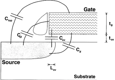
3.3.1 Capacitance Components
The various capacitance components that make up the gate-to-source capacitance (Cgs) of a MOSFET are illustrated in Figure 3-6. Cif is the inner fringing capacitance associated with the electric field emerging from the inner side of the of the source and ending at the underside of the polysilicon gate. C, is the overlap capacitance associated with the
Chapter 3. Inverse Doping Profiling from C-V Measurements top ^
t9
CSource
Lo
Substrate
Figure 3-6: The various components that make up the gate-to-source capacitance, Cgs. Also marked on the figure are the gate-source overlap Lo,, the oxide thickness to-, and the gate thickness tg.
voltage- and doping-dependent gate-to-source overlap region (L,,). Cof is the outer fringing capacitance associated with the electric field emerging from the side of the gate, going through the side-wall spacer and ending at the top of the source region. Finally, Cop is the capacitance due to the electric field lines emerging from the top of the gate, going through the first passivation layer and ending at the top of the source.
Cof and Ctop are virtually bias independent, being mainly determined by physical prop-erties of the MOSFET such as the the gate and oxide thickness (tg and to,), the gate length (Lg) and the choice of spacer and passivation layer dielectrics. Ctop is perhaps the smallest component of the total gate-to-source capacitance because of the relatively large distance the electric field lines need to travel from the top of the gate to the top of source. Ct0p was in fact ignored in most simple calculations until recently, when an analytical formula for it was proposed [33]:
Lg
Ctop = cox In (1 + t + t) (3.15)
where L9 is the polysilicon gate length and the use of Eox assumes an oxide passivation 40