Colloidal Electronics
by(Albert) Tianxiang Liu
B.S. Chemical Engineering, California institute of Technology, 2014
SUBMITTED TO THE DEPARTMENT OF CHEMICAL ENGINEERING IN PARTIAL FULFILLMENT OF THE REQUIREMENTS FOR THE DEGREE OF
DOCTOR OF PHILOSOPHY IN CHEMICAL ENGINEERING AT THE
MASSACHUSETTS INSTITUTE OF TECHNOLOGY July 2020
© 2020 Massachusetts Institute of Technology. All rights reserved.
Signature of author ... Department of Chemical Engineering July 27, 2020
Certified by ... Michael S. Strano Carbon P. Dubbs Professor of Chemical Engineering Thesis Supervisor
Accepted by ... Patrick S. Doyle Robert T. Haslam (1911) Professor of Chemical Engineering Graduate Officer
3
Colloidal Electronics
by(Albert) Tianxiang Liu
Submitted to the Department of Chemical Engineering
on July 27, 2020, in partial fulfillment of the requirements for the degree of Doctor of Philosophy in Chemical Engineering
Abstract
Arming nano-electronics with mobility extends artificial systems into traditionally inaccessible environments. Carbon nanotubes (1D), graphene (2D) and other low-dimensional materials with well-defined lattice structures can be incorporated into polymer microparticles, granting them unique electronic functions. The resulting colloidal electronic ‘cells’, comprised of microscopic circuits connecting artificial ‘organelles’ (e.g., generators, sensors, logic gates, etc.), combine the modularity of modern electronics with the characteristic mobility found in dispersive colloidal systems. Fundamental to colloidal electronics lie two challenges: (1) providing electrical energy to a microscopic system with limited footprint; and (2) developing energy efficient electronic devices and circuitries with low power consumption. In this context, my thesis introduces two concepts – Autoperforation and Asymmetric Chemical Doping – as means to fabricate and power electronic circuit elements on top of colloidal particles. These advances allow us to build the first colloidal electronic system that perform autonomous functions integrating energy harvesting, chemical detection and digital memory recording – all within a form-factor no larger than biological cells.
4
Acknowledgements
I am forever grateful to have had Michael as my graduate advisor, who have continually fostered my scientific curiosity and encouraged my research independence. The extent to which his support has shaped my academic career cannot be overstated. Michael’s positivity, creativity, and scientific leadership have played a critical role in my growth as a scientist.
I would like to thank Will Tisdale and Karthish Manthiram, for being a part of my Thesis Committee, for offering critical feedback at every step along the way, and for asking important questions to help me with my research and to steer me in the right direction. I would also like to thank Martin Bazant, Bill Deen, Jim Swan, Alan Hatton, and Klavs Jensen for their guidance and feedback on my thesis research.
During my time at MIT, I have had many memorable moments as a teacher. I am grateful for the support of Bill Deen and Martin Bazant during my time as a TA for 10.50, of Klavs Jensen and Michael during my time as a TA for 10.65, of Michael during my time as a project consultant for 10.26, and Benjamin Hansberry for the Teaching Development Fellow program.
I am extremely fortunate to have been surrounded by a group of talented colleagues within Michael’s group. I am particularly thankful to the help of Yuichiro Kunai, Anton Cottrill,
Sayalee Mahajan, Pingwei Liu, Jingfan Yang, Ge Zhang, and Allan Brooks. I would also like to thank the students whom I have had a good fortune to work with: Stephen Gibbs, Jamila Smith-Dell, Max Saccone, Linh Nguyen, Rafid Mollah, Yannick Eatmon, Paul Baynard, Ian Timothy, and Lexy LeMar.
5
My thesis work has also greatly benefitted from a number of collaborators: Marek Hampel and Tomás Palacios from MIT, Ana Pervan and Todd Murphey from Northwestern, Paul McEuen from Cornell, Josh Daymude Andrea Richa from Arizona State, Dan Goldman and Dana Randall from Georgia Tech.
I would also like to thank the following people who have helped me to navigate through career decisions: Michael, Karthish Manthiram, Connor Coley, Will Tisdale, Jim Swan, Bill Deen, Klavs Jensen, Kate Galloway, Ariel Furst, Crystal Chu, and Lennon Luo from MIT, Greg Fu, Mark Davis, John Seinfeld, Zhen-Gang Wang, and Max Saccone from Caltech, Ana Pervan and Todd Murphey from Northwestern, Josh Daymude from Arizona State, and Dana Randall from Georgia Tech.
The past six years would not have been possible without my former scientific advisors: Jack Roberts, Greg Fu, Mark Davis, Stacey Zones, Steve Sieck, Jim Lindberg, Andy Mobley, and Heriberto Hernandez-Soto. These mentors have been, are, and will always be a source of inspiration. I can only hope to provide my own students with a small fraction of what they have provided me.
I would not be where I am if it were not for my parents, Weimin Liu and Li Wang, and my partner, Stacey Fang. They have provided a tremendous amount of support in every way imaginable. For without their devotion, I would not have accomplished any of these, and without them, none of these accomplishments would have been meaningful.
6
Table of Contents
Abstract ... 3
Acknowledgements ... 4
Introduction to Colloidal Electronics ... 9
1.1 Colloidal State Machines: Autonomous Particles with On-Board Computation ... 14
1.1.1 What are Colloidal State Machines? ... 14
1.1.2 CSM Coagulation and Sedimentation ... 17
1.1.3 Materials-Enabled CSM Modules... 18
1.1.4 CSM Systems Integration ... 27
1.1.5 Control and Robotics of Autonomous CSMs ... 33
1.1.6 Application of CSMs ... 37
1.1.7 Conclusions and Outlook ... 40
1.2 Direct Electricity Generation Mediated by Molecular Interactions with Low Dimensional Carbon Materials – A Mechanistic Perspective ... 42
1.2.1 Motivations for Solvent Mediated Energy Harvesting Methods ... 42
1.2.2 Mechanistic Overview ... 45
1.2.3 Perspectives, Application Space, and Energy Metrics ... 112
1.3 References ... 124
Sustainable Power Sources Based on High Efficiency Thermopower Wave Devices ... 144
2.1 Background on Thermopower Wave Technology ... 145
2.2 High Efficiency Thermopower Wave Devices ... 146
2.3 References ... 160
Electrical Energy Generation via Reversible Chemical Doping on Carbon Nanotube Fibers ... 163
3.1 Background on Excess Thermopower... 164
3.2 From Thermopower Wave to Asymmetric Chemical Doping ... 166
3.3 Experimental Details ... 177
3.4 References ... 179
Observation of the Marcus Inverted Region of Electron Transfer from Asymmetric Chemical Doping of Pristine (n, m) Single-Walled Carbon Nanotubes ... 182
4.1 Background on Asymmetric Chemical Doping ... 183
7
4.3 Experimental Details ... 203
4.4 References ... 204
Solvent-Induced Electrocatalysis at an Asymmetric Carbon Interface ... 207
5.1 Asymmetric Chemical Doping to Drive Electrochemical Transformations ... 208
5.2 References ... 227
Autoperforation of Two-Dimensional Materials as Method to Prepare Electronic Colloids ... 229
5.1 Autoperforation of Two-Dimensional Materials for Generating Two Terminal Memristive Janus Particles ... 230
5.2 Autoperforation of Two-Dimensional Materials to Generate Colloidal State Machines Capable of Locomotion... 265
6.2.1 Patterned Pt Electrodeposition on Graphene Surfaces using Inkjet Printing ... 274
6.2.2 Pt-Coated Janus CSMs via Aligned Inkjet Printing and Autoperforation ... 280
6.2.3 Self-Driven Locomotion of Pt-Coated Janus Graphene-CSMs in H2O2 ... 281
6.2.3 Towards Navigation in a Complex Fluidic Network ... 283
6.2.4 Experimental Details ... 294
6.3 References ... 295
Collective Synchronization in Self-driven Chemo-mechanical Relaxation Oscillators ... 300
7.1 Background on Emergent Behavior and Relaxation Oscillators ... 300
7.2 The Physical Design that Results Synchronized Oscillation ... 302
7.3 An Analytical Model that Captures the Primary Mode of Oscillation ... 305
Outlook on Colloidal Electronics... 310
8.1 Across the Solid-Liquid Interface: Energy Harvesting for Distributed Colloidal Electronic Systems ... 311
8.2 Self-powered Electrocatalysis as Means of Interparticle & Particle-to-Cell Communication ... 314
8.2.1 Field-assisted Electro-reduction of CO2 to C2+ Products on Morphologically Controlled Metal Surfaces ... 315
8.2.2 MOF-Metal Hybrid Electrodes with Engineered Catalytic Pockets for Electro-Oxidative C-C Coupling ... 317
8.3 Low-power Nano-electronic Circuits and Their Incorporation into Microparticle Tracers to Enable Time-dependent Sensing and Continuous Information Recording ... 320
8.3.1 Fabrication of Vertically Aligned Memristor Arrays ... 320
8
8.3.3 Engineering Time-aware Colloidal Tracers for Time-dependent Continuous
Information Recording ... 323 8.4 Putting It All Together – Static (Equilibrium) and Dynamic (Non-equilibrium)
Assembly of Electronic Colloids into Integrated Electrical Networks ... 326 8.4.1 Top-down Integration of Colloidal Electronics into Functional Composites ... 326 8.4.2 Bottom-up Assembly of Colloidal Electronics into Artificial Efferent Neurons . 327 8.5 References ... 329
9
Chapter 1
Introduction to Colloidal Electronics
Articles that contribute to this chapter:
Liu, A. T.; Hempel, M.; Yang, J. F.; Pervan, A.; Koman, V. B.; Zhang, G.; Kozawa, D.; Murphey, T. D.; Palacios, T.; Strano, M. S. submitted
Liu, A. T.; Zhang, G.; Cottrill, A. L.; Kunai, Y.; Kaplan, A.; Liu, P.; Koman, V. B.; Strano, M. S. Advanced Energy Materials (2018), 8, 1802212
Liu, A. T.; Zhang, G.; Strano, M. S. Robotic Systems and Autonomous Platforms (2019), 389
Arming nano-electronics with mobility extends artificial systems into traditionally inaccessible environments. Carbon nanotubes (1D), graphene (2D) and other crystalline materials with well-defined lattice structures can be incorporated into polymer microparticles, granting them unique electronic functions.1 The resulting colloidal electronic ‘cells’ (ca. 100 µm in diameter), comprised of microscopic circuits connecting artificial ‘organelles’ (e.g., generators, sensors, logic gates, etc.), combine the modularity of modern electronics with the characteristic mobility found in dispersive colloidal systems. They perform autonomous functions integrating optical energy harvesting, chemical detection and digital memory recording – all within a form-factor no larger than biological cells.2
My thesis research seeks to advance device capabilities for individual colloidal electronic particles, and explore higher-order assemblies of these building-blocks into hierarchical colloidal
10
electronic matter (Figure 1-1). This research topic, positioned at the intersection between materials design, chemical catalysis, and electronic device fabrication, aims to address one central
challenge: Can we build materials the way nature builds us? Biological scaffolds are constructed with long-range order that spans many orders of magnitude, affording control checkpoints not only at the molecular (e.g., protein) level, but also on the micro- (e.g., organelle) and meso- (e.g., cellular) scales. The ability to create ‘tissue’-like colloidal electronic matter, consisting of heterogeneously integrated electronic ‘cells’, will enable access to complex functions observed previously only in biological systems (Figure 1-2).
Figure 1-1. Colloidal electronic matter assembled using individual electronic colloids. In colloidal electronics, nano-electronic devices are integrated into a colloidal microparticle,
conferring specific capabilities: energy harvesting (Chapter 2 – 4), communication (Chapter 5),
sensing and memory (Chapter 6). The assembly of colloidal electronic matter is discussed in Chapter 7.
11
Specifically, my thesis builds toward a paradigm of rational design and synthesis of colloidal
electronics by (1) developing in situ energy generation methods, (2) creating inter-particle
communication techniques suitable for autonomous systems at the cellular scale, (3) designing energy efficient colloidal electronic devices and circuits that bring macroscopic functions to the microscale, and (4) establishing protocols to assemble hierarchical colloidal scaffolds with long-range spatial order via a combination of top-down (e.g., 3D printing) and bottom-up (e.g., guided self-assembly) approaches.
By laying the foundation towards this new class of materials, my studies generate new opportunities in environmental monitoring, biomedical sensing, distributed computing and human-machine interface. In the context of human health, several task-oriented applications enabled by the colloidal electronic technology can be pursued in the future (Figure 2). For example, one can develop individual colloidal electronic devices capable of (a) localized electrochemical communication with neurons, (b) time-dependent data acquisition that maps the spatial composition of mammalian gut microbiota, and cooperative colloidal electronic systems that can (c) be processed into smart textiles for advanced diagnostics, or (d) self-assemble into artificial neurons that reestablish synaptic connections to alleviate symptoms of spinal cord injury or neuro-degenerative disorders. The future directions of colloidal electronics are expanded in further detail in the outlook sections of Chapter 8.
12
Figure 1-2. Task-oriented applications for individual (a, b) and ensemble (c, d) colloidal
electronic matter. (a) in situ electro-chemical communication to cells; (b) Location-dependent data acquisition; (c) integrated smart textile; (d) self-assembled artificial neuron.
Minimizing the invasiveness of electronic devices, both in a spatial and a temporal sense, has motivated innovations such as flexible electronics3,4 that establish intimate tissue connections, and
transient electronics5 that naturally decompose after their intended diagnostic window. Colloidal
electronics – with microscopic sizes that allow them to be dispersed in, and travel with, the
surrounding fluid to circulate and exit the body – represent the ultimate flexible and transient electronic system. The field of colloidal electronics aims to bring ubiquitous intelligence in the form of distributed systems. Fundamental to this new platform lie four challenges: (1) providing electrical energy to a microscopic system with limited footprint (ca. 1 picolitre or 10 × 10 × 10 µm3 in volume); (2) enabling inter-particle communication; (3) developing energy efficient devices and circuitries with low power requirements; and (4) forming a network of individual units that function in unison.
Electricity is the central energy currency in artificial programmable systems, akin to the role ATP plays in biological systems. The idea of creating a micrometer sized autonomous machine dates back to the 1950s,6 but was only (partially) realized over half a century later,2 in part due to the
13
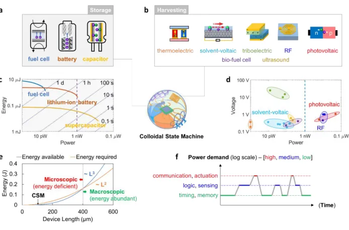
difficulties associated with active energy generation at the micrometer scale. Chemists and materials scientists have developed ‘molecular machines’ (ca. 1 nm) and ‘active matter’ (ca. 100 nm), which have been externally powered by either stochastic thermal interactions or global electromagnetic ‘tethers’, limiting the potential for these systems to achieve self-driven control. On the electronics side, the continuous shrinkage of semiconductor device footprint has given rise to ‘micro-robots’ (ca. 1 cm) and ‘smart dusts’ (ca. 1 mm). For characteristic device sizes (L) less than 100 µm, however, the mismatch between the amount of energy stored onboard (~ L3) and that required for basic device operations (~ L2) is prohibitive (Figure 1-3).7 Therefore, to provide
colloidal electronics regular access to onboard electricity, an effective active energy harvesting method is essential.7
Figure 1-3. Energy supply and demand plotted for artificial autonomous systems at various scales.
For devices with characteristic lengths under 100 µm, current energy storage and harvesting techniques are insufficient to power microsystems continuously.
To bridge this energy gap, the first part of my thesis explores different liquid-based energy harvesting methods more broadly known as the ‘solvo-voltaic’ effect,8 a phenomenon whereby
14
various local energy inputs are converted into electricity within a quantum-confined nanostructure (e.g., single-walled carbon nanotube, or SWCNT) by virtue of interactions with the surrounding solvent molecules. This technique stands out as a promising candidate to complement existing energy generation schemes like the photovoltaics, whose utility is diminished where visible light is not present. In the following two sections, I introduce one sub-type of colloidal electronics – Colloidal State Machines (CSMs), and present several ‘solvo-voltaic’ mechanisms in the literature by which electricity can be directly harvested from the ambient environment.
1.1 Colloidal State Machines: Autonomous Particles with On-Board Computation
A machine has components that work together to accomplish a task. Colloids are particles, usually less than 100 µm, that are small enough as to not settle out of solution. Colloidal State Machines (CSMs) are particles capable of functions such as sensing, computation, communication,
locomotion, and energy management all controlled by the particle itself. Their design and synthesis
is an emerging area of materials science research. Many CSM systems anticipate synthetic versions of biological cells in autonomy and may find ultimate utility in bringing these specialized functions to previously inaccessible locations. This perspective examines the emerging literature and highlights certain design principles and strategies towards the realization of CSMs. Potential applications to medicine; environmental monitoring; and geological, astrophysical and undersea exploration are highlighted.
1.1.1 What are Colloidal State Machines?
Colloidal State Machines (CSMs) are particle systems capable of autonomous functions, with
examples only recently emerging from the electronics and robotics literature.2 Autonomy in this setting is defined as the ability for machines to make decisions (or ‘compute’), without external
15
actuation and supervision. CSMs are distinct from ‘micro-robotic’ systems9, since the latter refer
to mm to cm scale systems. They are also distinct from ‘nano-robotics’, and similarly ‘active matter’, since these terms most often describe a device controlled from a distance using magnetic fields or light, with an infrastructure off the entity itself. The concept of a puppet can be used to distinguish where computation and decision making are designed to occur, with CSMs designed for these tasks to be on the particle itself. Nature has evolved micron-sized entities capable of autonomy and computation. CSMs embody this new objective, harnessing emerging developments in nanofabrication, micro- and nano-electronics, materials science and autonomous control. The motivating vision is to extend nanoelectronics into traditionally inaccessible locations using colloidal microparticles.
CSMs follow a conceptual path from past efforts to miniaturize both electronics and robotics (Figure 1-4). Although remarkable progress has been made with silicon-based microsystems (sometimes referred to as ‘Smart Dust’)10 that integrate sensing, computation, and communication,
these microsystems are static and have volumes typically larger than 1 mm3, which limit their potential application compared to CSMs. As a result, successful implementations of microscale electronic systems remain elusive in medicine except for environments where volume is less of a constraint, such as the mammalian digestive tract.11 In contrast, CSMs are envisioned as autonomous, self-contained machines that allow modular, programmable functions, all embedded on substrates that enable mobility in surrounding media, with volumes at least 1000 times smaller than today’s silicon-based approaches.
Just like any biological cell, a CSM cannot function without a suite of well-coordinated ‘organelles’. We surveyed several early examples of CSMs in literature,1,2,12-15 and identified that
16
sensors for information input, (2) a central processing unit for logic computation and data storage, (3) communication channels (e.g., between neighboring devices for information transfer), (4) modes of actuation and locomotion, and (5) an on-board energy source (harvesting and/or storage) to power these circuit operations (Figure 1-4). In this perspective, we present the state-of-the-art in these five fundamental building blocks in the context of CSMs; an account of the progress that has been made; and a forward-looking vision towards building prototype electronic devices onto a colloidal particulate platform.
Figure 1-4. Colloidal State Machines (CSM) – concept and prototypes from the literature. (a)
Schematic illustration of a CSM, prepared by Betsy Skrip. Scale bar, 50 µm. (b) Schematic illustration of an early CSM prototype being used for analyte and light detection inside a vapor chamber.2 Left: Electrical circuit diagram of the CSM. The photodiode converts light into current, which turns on the memristor if and only if the chemiresistor detects a prescribed analyte. Right: Top view optical micrograph of the CSM used. Scale bar, 50 µm. Reproduced with permission.2
Copyright 2018 Nature Publishing Group. (c) Block diagram for the CSM summarizing the combinational logic. The initial memory state OFF changes to ON only in the presence of both chemical and light signals. Reproduced with permission.2 Copyright 2018 Nature Publishing Group.
17
1.1.2 CSM Coagulation and Sedimentation
1.1.2.1 CSM Coagulation – Colloidal Stability
An important factor for a colloidal system lies in its stability, which in general depends on particle charges and coating chemistry. Lyophilic colloids, which exhibit a high force of attraction between the particles and their embedded liquid, for instance, are known to result in very stable colloidal solutions (e.g., starch and proteins). These solvent-loving molecules, when adsorbed onto the surface of the particle, may provide steric or entropic stabilization.16 The concept of relative stability is important when it comes to CSM design,
because as long as a CSM remains largely suspended throughout its duty cycle, one can treat this dispersion as ‘relatively stable’ – an acceptable condition for many applications.
With proper selection of surface chemistry and dispersion solution, CSMs can be made stable in solution on the order of minutes to hours, long enough for most envisioned applications.
1.1.2.2 CSM Sedimentation – Particle Buoyancy
For CSM systems that do not coagulate, it is also important to consider whether each CSM particle can be individually suspended without settling out. The study of the translation of these nearly-neutrally-buoyant particles with size scales commensurate to that of the surrounding turbulence are often restricted to ideal spheres, despite the scarcity of regular shapes in such processes.
The full analytical equation of motion for spherical particles in an unsteady flow (i.e., the Maxey-Riley equation) has been derived in the Stokes regime.17 Despite its simplicity, this
18
model has been very effective in understanding CSM sedimentation behavior, not only in aqueous environments, but also in air. In the context of ‘aerosolizable electronics’, for example, the Maxey-Riley equation of motion has successfully modeled the transient behavior of CSM aerosol particles lauched into the vapor phase using a nebulizer for environmental monitoring applications.2 It predicts, for example, that CSMs below 100 µm in size can exhibit settling rates on the order of minutes or higher.
1.1.3 Materials-Enabled CSM Modules
Herein, we break down complex CSM operations into five fundamental modules (i.e., computation, sensing, communication, locomotion, and energy management) and analyze those enabling technologies that are promising for CSM applications.
1.1.3.1 Logic and Computing
Computation is at the core of most electronic systems. It processes input signals from sensors, stores relevant information, and generates output signals in response. Silicon-based electronics is the cheapest, most reliable, and smallest option to build integrated circuits. Due to continued transistor scaling, today transistors have nanometer-scale dimensions with densities of 23 transistors/µm2 while consuming about 1.5 pW/MHz each.18 Several microsystems approaching the size of a CSM have been demonstrated using silicon chips for computation (Table 1-1), which target biomedical applications,19
environmental sensing12 and object verification20 and range in power from 0.4 nW to 10 µW.
19
Low-dimensional materials like carbon nanotubes and 2D materials have been explored extensively in recent years given their favorable electrostatics and high carrier mobility.21 Transistors based on 2D materials and carbon nanotubes with promising device characteristics have been fabricated, enabling the development of more complex circuits.22 However, electronics based on these materials are still in their infancy and cannot compete with silicon in terms of cost, reliability, and system complexity at present. In the near future, silicon should be the primary choice to bring computing capabilities to CSMs.
Herein, we break down complex CSM operations into five fundamental modules (i.e., computation, sensing, communication, locomotion, and energy management) and analyze those enabling technologies that are promising for CSM applications.
Table 1-1. Example of microsystems that use silicon chips for computation.
Microsystem Details Computation Communication
Year Application Power Size
[µm] Node
Comple xity
Mod
ality Medium Mode Distance
1997 Sensor
networks23 400 nW
~300x30
0x300 n/a n/a Light Air Passive 2 m
2004 RFID tags20 1.5 µW 400x400
x60
180
nm medium RF Air Passive 1.2 mm
2013 Neural
sensor24 10.5 µW
250x500 x ?
65
nm medium RF Air Passive 1 mm
2014 Pressure
sensor25 5.3 nW
1200x82 5x ?
180
nm high RF Water+Air Active 10 cm
2015 Neural
sensor26,27 0.9 µW
800x800
x800 n/a n/a US Water Passive 50 mm
2016 Chemical
sensing12 0.4 nW
200x100 x10
180
nm low n/a n/a n/a n/a
2017 Cell
monitor14 n/a 25x25x ? n/a n/a RF Water Passive 25 µm
2017 Glucose
sensor28 63 nW
200x200 x100
65
nm medium RF Tissue Passive 1.3 mm
2018 Neural
stimulation29 27 µW
200x200 x100
130
nm medium n/a n/a n/a n/a
2018 Neural
sensor13 1 µW
57x250x 330
180
20
1.1.3.2 Sensing
Sensing plays a central role in most microsystems, allowing them to be aware of their location, environment, and neighbors, and subsequently triggering signaling and downstream responses. In the context of CSMs, a need for modular integration renders electric sensors the most relevant. While silicon-based sensors are the easiest to integrate with logic, silicon transistors are not ideal for many sensing applications. As a result, it is important to integrate new materials. However, there are many new materials and mechanisms that can be used to make microscale electrical sensors for CSM-type systems, resulting in a fairly broad field that has been subject to extensive analyses.30
1.1.3.3 Communication
Communication between microsystems using electromagnetic, ultrasonic, optical and chemical means are summarized in Figure 1-5. Radio frequency (RF) communication is the standard choice for many technologies, yet antennas become increasingly inefficient when scaled down. Most reported RF systems at the sub-mm scale thus communicate data passively by backscattering the incoming signal, especially for medical applications.31 Similarly, the lowest power consumption in ultrasound (US) systems – best-suited for aqueous media such as water and biological tissues – is achieved when information is transmitted back passively. This approach has been used to build a neural recording device32 capable of transmitting data to a receiver 9 mm away. Light can also be used to communicate between CSMs, either by active light emission using light emitting diodes
2018 Temp.
sensor19 16 nW
360x400 x280
55
21
(LED) or through indirect means such as modulating fluorescence or reflection of light.33
In contrast to RF, optical systems scale well into the 1 to 100 µm range, although such communication is only feasible in transparent media such as water or air, and only locally.
A less conventional and little explored method of communication is through the emission and diffusion of molecules which serve as information carriers. Chemical communication is prevalent in nature, though it is slow and has a low bandwidth in contrast to the previously discussed modalities.34 For applications with relaxed timing and sparse information content, however, this may be a viable option. One way to implement CSMs with chemical communication is to equip them with molecule reservoirs that only open when certain conditions are met.35
There are several communication modalities available for CSMs under 100 µm, subject to environmental constraints. The decision on which technology should be implemented also depends on the communication mode, such as centralized base-to-unit communication or decentralized unit-to-unit communication. In general, the latter is more challenging due to limited on-board transmission power. However, in the context of CSMs, combining these two modes into what is known as ‘asymmetric communication’ presents further opportunities.
22
Figure 1-5. Overview of four communication modalities. (a) Light sources such as light emitting
diodes can be used for optical communication. (b) Electromagnetic (EM) communication can be achieved by using small coils that either actively emit EM waves or backscatter the sender’s signal. The small footprint of the CSM typically prevents the integration of far field antennas, which will limit EM to the near-field. (c) Ultrasound can be employed for communication. The simplest way is to use piezo crystals that interact with the waves and are able to backscatter the signal from the sender selectively. (d) Molecular diffusion may be used to transmit information by controlling the amount and type of specific molecules.
1.1.3.3 Actuation and Locomotion
The ability to autonomously actuate differentiates CSMs from conventional SoCs. Scaling physical systems down to microscopic dimensions causes surface-born interactions, such as surface tension, drag, and adhesion, to dominate over volumetric bulk effects, such as mass and inertia.36 One direct consequence is the optimal actuation strategies with which CSMs operate. In these length regimes, actuation mechanisms like chemical adhesion and surface forces become appealing choices, which scale more favorably than most
23
mechanical grippers.36 In order to possess true autonomy, the operation of CSMs must be
enabled by locally-stimulated actuators on board. Promising candidates include polymer- and gel-based actuators37 and thin film bimorphs38, the latter being especially preferable given their short response times.
Micro-swimmers generally fall into two categories: mechanical or chemical. The major challenge of microscale locomotion based on mechanical actuation arises from the kinetic
reversibility: for tiny particles (a10 m ) swimming in water, Re is typically much less than 1. This dictates that any micro-swimmer actuating in a cyclical fashion will have no net motion in a Newtonian fluid,39 a formidable hurdle to overcome for many mechanical
micro-swimmers.
In contrast, a chemical micro-swimmer does not require moving parts to move through a medium.40 One of the earliest examples of such autonomous motion was the Pt-Au bimetallic rod,41 from which various self-propulsion mechanisms have been explored. These include, but are not limited to: bubble propulsion,42 self-electrophoresis,41
self-diffusiophoresis,43 self-thermophoresis,44 and self-acoustophoresis45. Even so, a generalizable design rule for guided locomotion to enable programmable CSM chemotaxis and phototaxis beyond proof-of-concept environments has yet to be discovered.
1.1.3.3 Energy Harvesting and Storage
Electric energy is critical to power functions like information processing, actuation, and communication. It is not surprising therefore that energy supply represents one of the greatest challenges for CSMs. Figure 1-6e plots the energy demand for a standard computation and the energy available as a function of device characteristic length a . A
24
picoliter (1000 µm3) energy module comprised of the best commercial lithium-ion battery
would only be able to power a 100 nW load for roughly 25 seconds (2500 nW·s). There is thus a clear energy gap to bridge, creating opportunities for advanced materials.
Figure 1-6. Energy harvesting and storage techniques relevant for Colloidal State Machines. (a, b) Potentially feasible electrical power sources on the scale of CSMs, categorized by mechanism,
as storage (a) or harvesting (b) devices. (c) Ragone plot of energy storage devices at a limited volume of 1 pL. The parallel dashed lines represent the time of discharge. For example, if we discharge a Li-ion battery at 1 nW power, we follow the purple vertical line up and encounter the curve for battery between 1 h and 100 s, which means the battery will be fully discharged in several hundred seconds. The plot is based on a conservative estimation of the energy and power densities, with data from Pikul et. al.,46 which also shows that with an optimized configuration and structure
25
of electrodes, the maximum accessible power density may be boosted by 10 times.46 (d)
Voltage-power characteristics of energy harvesting devices. The Voltage-power output is estimated for a structure with 600 µm2 surface area, which is the maximum attainable for a 10 × 10 × 10 µm3 CSM. Solar cell is supposed to have 10% efficiency and put under 1 sun illumination (about 1 kW/m2). (e) Estimated energy required for standard computation18 (20 transistors per µm2 with each transistor consuming 5 nW at 3.4 GHz for computation time of 10 s) and electrochemically stored energy (2.5 nJ·µm3) plotted as a function of device length. (f) Example duty cycle of a CSM, utilizing different energy sources at different power demands.
Some micro-batteries with interdigital electrodes and 3-D current collectors may possess power density 1 order of magnitude higher than the commercial lithium-ion batteries, with sacrificed energy density.46 Nonetheless, with a system volume of 1 pL, batteries supply less than 0.1 µW, which is sufficient for standby circuits but not enough for communication. Alternatively, supercapacitors can offer energy and power densities of up to 0.4 nJ·µm-3 and 10 pW·µm-3 respectively,47 while regular dielectric capacitors offer much lower areal energy densities of 25-400 fJ·µm-2 but reach much higher power densities of up to 400 nW·µm-2 due to the quick discharge48 – ideal for short bursts of communication or other brief, high power tasks (Table 2). The Ragone plot (Figure
1-6c) visualizes this trade-off between power and energy density.
Table 1-2. Energy storage technologies relevant in the context of CSM.
Technology Energy Density Power Density Vmax Ref Comments
Lithium-Ion Battery 2.5 nJ/μm3 0.8 pW/μm3 3-4 V 49 Assuming full discharge in 1h
Thin-film Battery 2-14 nJ/μm3 0.5-4 pW/μm3 1-4 V 50 Assuming full discharge in 1h
Super capacitor 0.1-0.4 nJ/µm3 1-10 pW/µm3 1-3 V 47
26
To achieve partial or complete autonomy, prior CSM demonstrations have often relied on external energy harvesting. Chemical fuels have the highest energy density (e.g., 31.3 nJ·µm-3 in ethanol as opposed to 2.5 nJ·µm-3 in lithium ion batteries) and therefore represent a promising method to power micro-scale electronics. One example is thermopower waves.52 This technique requires no moving parts, and is capable of
producing a pulse of high voltage (> 5 V) and power (0.11 nW µm−3). Biotic and abiotic fuel cells have also been explored for direct conversion of chemical energy, providing a typical power density of 1 pW·µm-3 and a supply voltage of 0.5 V. RF energy harvesters can deliver a high-power density of 10-400 pW·µm-2 at a few millimeters distance and total transmit powers in the range of 50-2000 mW. However, these numbers are only rough guides since smaller coils (< 100 µm) typically operate in the near-field regime and down-scaling likely results in lower efficiencies (Table 1-3). The photovoltaic effect has been used extensively in autonomous microsystems for ambient and in-vivo applications.13 Given a pico-liter colloidal device, about 60 nW of power could be generated, assuming a 10% efficient solar cell and direct sun light (~1 nW·µm-2). For indoor applications, light sources are about 200 times less powerful53 and would result in a usable power of 0.3 nW for the same device.
Table 1-3. Energy harvesting technologies relevant in the context of CSM.
Technology Medium and Distance Transmit Power Receiving Power Voltage Footprint of coil/piezo/LED Ref RF coil 1.2 mm air 300 mW 10 pW/µm2 0.5 V 400 x 400 μm 20 RF coil 1 mm air 50 mW 80 pW/µm2 1.07 V 250 x 500 μm 24
RF coil 3 mm air + 4 mm muscle 2000 mW 400 pW/µm2 1.3 V 200 x 200 μm 29
27
Ultrasound 50 mm water 7.2 mW/cm2 0.35 pW/µm3 0.46 V 800 x 800 x 800 um 27
Ultrasound 3 mm muscle 100 mW/cm2 0.28 pW/µm3 0.6-1.1 V 1 x 1 x 1.4 mm 54
Solar Cell air 100 mW/cm2 1.1 pW/µm2 0.5 V 0.07 mm2 25
Solar Cell 4.75 mm pig skin 325 mW/cm2 160 pW/µm2 0.45 V 2 x 2 mm 55
Solar Cell 1.3 mm pig skin 190 mW/cm2 3.5 pW/µm2 -0.3 V 135 x 135 um 28
Solar Cell Air (microscope) 50 mW/cm2 200 pW/µm2 1.0 V 50 x 100 um 13
Solar Cell 15.6 cm air 4.5 mW/cm2 0.4 pW/µm2 0.65 V 180 x 230 um 19
Finally, there are emerging technologies that may be used to power colloidal systems in the future. A promising candidate is solvent interaction harvesting (or ‘solvovoltaics’8), which is particularly relevant to CSMs because it taps into their surrounding solvent environment. Alternatively, (mechanical) triboelectric generators could deliver power density in the range of 0.1 pW·µm-3 and high voltages on the order of 10 V.56
As shown in Figure 1-6c and d, given the above strengths and weaknesses of each energy source, a CSM will likely integrate multiple energy storage and harvesting modules to accommodate different electric functions and situations. Assigning appropriate electricity generators to a specific purpose is the key to navigating the CSM across a potentially anisotropic energy landscape (Figure 1-6f).
1.1.4 CSM Systems Integration
The goal of CSM integration is to build complex, autonomous systems from individual building blocks, analogous to combining individual “organelles” (e.g., “nucleus” as CPUs, “mitochondria” as energy harvesters, “flagella” as actuators, etc.) into higher-order “cells”.
1.1.4.1 Top-down Technologies
Lithography is a staple technique for high-density monolithic circuits. It can pattern up to 300 mm wafers but requires flat substrates and a cleanroom environment. Optical
28
immersion lithography with self-aligned quadruple patterning achieves resolutions of 10 nm in industrial production.57 Electron beam lithography, commonly used in academic settings, can even realize features down to 5 nm without the need for a photomask, however at lower throughput.57 As a result, photo- and electron beam lithography will play an integral part in the fabrication of CSM building blocks, especially those requiring patterns on the nanometer scale at large scale. One recent example is Koman et. al’s 2D material CSMs, which were mass fabricated using photolithography (Figure 1-7b).2 Specifically, each individual machine, capable of combinational logic (Figure 1-7c), contains three 2D components: a MoS2/WSe2 photodiode as the power source, a MoS2 chemiresistor as the
29
Figure 1-7. Selected examples for device integration relevant for colloidal electronic applications. (a) Schematic illustration for the assembling process of ink-jet printed polystyrene beads into
aggregated dome-shaped arrays. Inset: Scanning electron micrograph (SEM) of one such printed polystyrene micro-dome. Scalebar, 5 µm. Reproduced with permission.58 Copyright 2014 Wiley VCH. (b) High throughput in-air microfluidic ink-jet printing of micro-suspensions of multiple compositions. Left: Schematic illustration of the technique that generates core-shell structures with inner (blue) and outer (red) layers. Middle: Spherical particle suspensions viewed via optical microscopy. Right: Multi-material (alginate-dextran-tyramine in H2O) core-shell particles. All
scalebars, 50 µm. Reproduced with permission.59 Copyright 2018 American Association for the Advancement of Science. (c) Ink-jet printing of CSM particles consist of graphene encapsulated memristor arrays. Left: Optical image (inset: micrograph) of the printed microparticles. Middle: Top view of electrical testing a single graphene-encapsulated phosphorene-polystyrene composite microparticle (after solution lift-off and recapture) in a probe station. Bottom-right inset: schematic illustration of the cross-sectional view of the micro-particle – phosphorene nanoflakes (blue) inside a polystyrene matrix (yellow) forms arrays of memristor elements between the two encapsulating layers of graphene (black). Top-right: A 15-bit microparticle memristor array written via electronic probes. Vertical conductivity map (red – ON, clear – OFF) with the shape “M” overlaid on top of the microparticle tested. All scale bars, 50 µm. Reproduced with permission.1 Copyright 2018 Nature Publishing Group. (d) Left: Schematic illustration of transfer printing. Top-left: Laminating a stamp against a donor substrate (blue) and then quickly peeling it away, pulling the microstructures from the donor substrate onto the stamp. Bottom-left: Contacting the stamp to the receiving substrate (red) and then slowly peeling it away transfers the microstructures from the stamp to the receiver (red). Reproduced with permission.60 Copyright
30
2006 Nature Publishing Group. Right: False-colored SEM images of an array of devices, shown in sequence, after undercut etching (top-right), after removal of a single device from the donor wafer (middle-right), and after transfer printing of this device onto a receiving substrate
(bottom-right). Scalebar, 50 µm. Reproduced with permission.61 Copyright 2017 National Academy of Sciences. (e) Optical micrographs showing fracture and crack propagation of the graphene layers around a single polymer disk. Scalebar, 100 µm. Reproduced with permission.1 Copyright 2018
Nature Publishing Group. (f) Time-elapsed optical micrographs of an autoperforated graphene-encapsulated polymer disk rotating and translating in solution in a laminar flow field. Scalebar, 100 µm. Reproduced with permission.1 Copyright 2018 Nature Publishing Group. (g) Time-elapsed optical micrographs during evaporation of the toluene, showing the emulsion encapsulation process. Particles freely diffuse about the surface of the droplet until, as more toluene evaporates, they touch one another, forming a spherical packing. Deformation of the interface then leads to a rapid rearrangement to a cluster. Scalebar, 2 µm. Reproduced with permission.62 Copyright 2003 American Association for the Advancement of Science. (h) Bright-field (bottom panels) and schematic images (top panels) showing colloidal “molecules” self-assembled from “patchy” particles pre-programed with complementary green and red DNA patches. Supra-colloidal “molecules” AB2, AB3 and AB4 are formed by mixing red monovalent with green divalent, trivalent and tetravalent particles. If complementary divalent particles are mixed, linear alternating “polymer” chains spontaneously assemble. Scalebar, 2 µm. Reproduced with permission.63 Copyright 2012 Nature Publishing Group.
With recent advances in precision printing, additive manufacturing rises as a viable and relatively inexpensive alternative to traditional manufacturing methods. Unlike lithography, additive printing builds complex scaffolds through deposition, layer upon
31
layer. State-of-the-art printing processes achieve a minimum feature size of about 1 µm with alignment accuracies of several micrometers and printing speeds of about 1 m/s (Figure 1-7a, b).64 For features that do not require nanometer precision, printing is inexpensive and compatible with a large variety of materials (e.g., nano- and microparticles of various shapes, thermoplastics, ceramics, polymer composites, low-dimensional materials, etc.). In practice, various ‘inks’ have been used to establish active or passive circuit elements, such as transistors, capacitors, resistors, memristors, etc. (Figure 1-7c),1 suggesting printing as a complementary tool for CSM fabrication.59
Another approach for top-down device assembly involves the combination of separate as-made modules, broadly categorized here as heterogeneous integration. This encompasses a wide spectrum of techniques, all the way from traditional integrated circuit methods like wire bonding, flip chip reflow soldering, through-chip via, and wafer bonding to recent materials transfer innovations such as fluidic self-assembly,65 dry transfer printing (Figure
1-7d),60 and wafer-scale layer-by-layer assembly.66 Specifically, the combination of dry-transfer printing and device fabrication on sacrificial layers such as silicon on insulator may prove indispensable to CSMs. On one hand, it allows picking the best material for each building block, e.g., silicon for computation, III-V semiconductors for LEDs. On the other hand, this approach decouples fabrication constraints such as high temperature processing or chemical compatibility or each building block (Figure 1-7d).
1.1.4.2 Bottom-up Technologies
It is well-understood that material fracture can be controlled using a prescribed strain field, and the governing Griffith criterion has been demonstrated to operate down to the
32
nanometer limit within 2D lattices such as graphene.67 Recently, Liu et al. successfully
implemented the strategy of strain induced guided “automatic perforation” (or “autoperforation”) on 2D material sheets (monolayer graphene, MoS2 and hBN),
demonstrating the feasibility of using controlled defect self-assembly as a reliable and scalable nanofabrication method applicable to the production of electronic colloids.1 This “autoperforation” strategy forms the basis for various types of autonomous micro-electronic devices capable of analyte detection and memory storage (Figure 1-7c).1 Given that most of our current electronic material systems and fabrication methods are optimized for circuits in 2D, self-folding strategies, such as the ones inspired from origami and kirigami, have opened the door to creating complex 3D structures using planar fabrication techniques.38 Recent work has demonstrated successful folding of polymers,68 shape-memory alloys,69 and 2D materials38 at various length scales. Origami robots capable of autonomous actuation,38 supervised locomotion70 and reprogrammable self-assembly71
have also been fabricated en masse. With its inherent scale-free character, origami as a framework for metamaterial design has found utility across many geometric scales (mm, µm, nm).
Self-assembly is a process in which a system of pre-existing components spontaneously organizes into an ordered structure through no external supervision. Well-defined structures can be synthesized via processes such as emulsion encapsulation (Figure 1-7g)62 and DNA hybridization (Figure 1-7h).63 Alternatively, colloids can be precisely organized and linked by a “lock and key” mechanism,72 patchy surface hydrophobicity,73 or wetting
forces (“colloidal fusion”).74 On the other hand, dynamic, or out-of-equilibrium, assembly
33
colloids is constantly growing, programmed-clustering of individual parts into CSMs with full electronic autonomy is still at its naissance.
1.1.5 Control and Robotics of Autonomous CSMs
1.1.5.1 Control of CSMs
Control is traditionally implemented through reconfigurable computing to calculate optimal or near-optimal decisions based on an objective. 76 However, as a system shrinks, reconfigurable computing takes a greater percentage of physical volume and energy budget, eventually becoming impractical. As a result, control of CSMs will be constrained to use limited computational resources, relying on the material properties of CSMs to implicitly perform operations normally reserved for computing.
Consequently, the control authority of CSMs (in the form of simple circuits,2 logical operators, and individual elements of nonvolatile memory1), will be internally represented in terms of discrete states – despite CSMs operating in and interacting with continuous environments. Systems with a combination of continuous and discrete components are
hybrid systems.77 Figure 1-8a shows a control architecture – a result of a hybrid, optimization-based approach78 – capable of moving a CSM to a specified location. The CSM autonomously achieves its goal in continuous space, using only discrete actuation, discrete sensing, and a few logical operators.78
34
Figure 1-8. (a) Model-based control. Left. A planar environment with six different chemical
sources. A CSM is able to locomote by choosing one of seven different control modes: being attracted toward a chemical potential at one of the six different sources (u1, u2, u3, u4, u5, u6), or
staying still (u0). The goal of the device is to go toward point P. Middle. A continuous control
policy that indicates which control mode (shown with different colors) to use at each location in the 2D environment. The discrete control output is a function of continuous input variables u(x,y).
35
be differentiated using chemical comparators. The discrete control output is a function of discrete input regions u(r). Reproduced with permission.78 (b) The ensemble of CSMs (shown in pink) needs to find an energy source (the blue object), but in doing so diffuses. As a consequence, the CSMs need to then exploit environmental characteristics (the yellow pocket in the environment) to reassemble themselves into a non-diffuse ensemble. (c) Simulated data of individual particles (top) can be simplified to the ensemble's motion (left) which gets abstracted as three modes of transport (middle) that can then be encoded in a finite state machine (right) on board each CSM. The small number of behaviors that describe the complex dynamics lead to minimal computation elements the CSMs will need to employ to execute control. (d) An illustration of a sequence of rollouts that could enable CSMs to learn in a massively parallel fashion. Starting from an initial set of randomized rollouts, through intercell communication the policy can be updated, eventually leading to a policy that successfully encapsulates a mass.
If individual CSMs can be controlled, ensembles of CSMs should be able to achieve greater objectives. The control of systems of simple agents has been explored in many areas, such as “shortcut bridging” in army ants, where a stochastic, distributed algorithm enabled
particles to self-assemble into bridges optimized for length and cost.79 Similar global behaviors have been demonstrated in algorithms for compression or expansion, and separation or integration of heterogeneous agents.80 Nevertheless, there are fundamental
limitations on what a group of autonomous, memoryless mobile robots can achieve.81,82
1.1.5.2 Emergent Behavior and Learning in CSMs
To make control decisions, a CSM directly modeling physical states is impractical. Instead, we assume the model is an emergent phenomenon, implying that an
36
ensemble of CSMs must detect, and exploit, emergent behavior to accomplish its goals. In
Figure 1-8b, CSMs search for a blue object but diffuse as they do so. They must detect
and exploit the yellow energy potential to avoid dispersion.
To discover emergence, the ensemble might assume a very limited model, which involves only a small number of unknown behaviors. In Figure 1-8c, a simulated ensemble of individually stochastic CSMs on average move in only a few ways. There are three distinct dynamic behaviors (translating left, up, and right) that the ensemble can choose based on sensory inputs. Once these emergent behaviors are identified,83 they can be used in
different combinations to execute tasks.
Despite computational limitations of individual CSMs, an ensemble is highly parallelizable – many individuals can be used in parallel reinforcement learning.84 This enables the
ensemble to update policies over multiple attempts, in response to varying task success. As illustrated in Figure 1-8d, devices of different colors (representing distinct rollouts) attempt to encapsulate an object. Later rollouts of CSMs update their policies in response to rewards reaped by earlier attempts, enabling ensembles to learn.
Even with limited computation, the examples above illustrate how CSMs can exhibit emergent intelligence. As a result, rather than autonomy being a consequence of exquisite sensing, actuation, and computation, autonomy will be the result of flexible interactions between the colloidal particle and its environment.
37
1.1.6 Application of CSMs
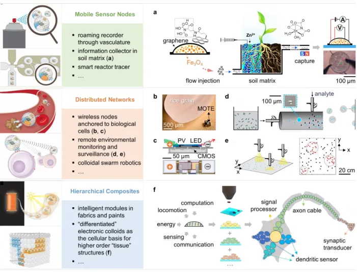
Autonomous Colloidal State Machines collect, manipulate, store, and exchange information without external supervision.2,85 When the highly-dispersed nature inherent to a colloidal system interfaces with the autonomy and programmability that stem from electronics, new capabilities emerge. We broadly classify these applications in three functional areas.
On the one hand CSMs can be used for signal processing and transduction from enclosed spaces – like the mammalian vasculature, microfluidic channels, and chemical/biosynthetic reactors2 – as
well as recording from remote locations like oil and gas conduits, rock crevices, waterbodies,1 soil
matrix,1 or the atmosphere. Operating at cellular dimensions13,19 enables a different paradigm of human-matter interaction, allowing people to intimately interact with microscopic systems like never before (Figure 1-9e).
38
Figure 1-9. Demonstrated and potential applications for Colloidal State Machines. (a) Schematic
illustration of the deployment of surface-functionalized colloidal electronic microparticles as chemical probes to detect and record the presence of various species, such as Zn2+ ions in the soil matrix. These colloidal devices can be retrieved via magnetic capture for electrical and optical readout. Inset: Optical micrograph of the colloidal electronic particle during the electrical readout. Scale bar, 100 µm. Reproduced with permission.1 Copyright 2018 Nature Publishing Group. (b) A laser-powered 0.04 mm3 16 nW wireless sensor MOTE with integrated central processing and optical communication units placed by a grain of rice. This system is capable of accurate cellular temperature measurement in vitro. Scale bar, 500 µm. Reproduced with permission.19 Copyright 2018 IEEE. (c) A 250 μm × 57 μm 1 μW MOTE capable of capable of capturing and encoding
39
neural signals before transmitting the encoded signals. This system is powered by and communicates through an optical interface. Scale bar, 50 µm. Reproduced with permission.13 Copyright 2018 IEEE. (d) Experimental schematic showing remote detection and memory storage using CSMs aerosolized from their original colloidal suspension. The left nebulizer injects CSMs (teal squares) across the enclosed tube injected with an analyte (dark blue droplets) using the top nebulizer. CSMs are collected on the collector on the right, exposed to light, and their memory states are queried afterwards. Scale bar, 100 µm. Reproduced with permission.2 Copyright 2018 Nature Publishing Group. (e) Left: Schematic illustration of large area sensing using CSMs. Analytes (yellow) are sprayed at three locations over an area with previously dispersed CSMs (teal squares). Right: Digitized positions of distributed CSMs. Dashed circles are eye guides, highlighting three areas exposed to the analyte. Turn ON responses (red) can be seen for those CSMs exposed to the analyte, as oppose to those that have not (OFF state, black). Scale bar, 20 cm. Reproduced with permission.2 Copyright 2018 Nature Publishing Group. (f) Schematics
illustrating the concept of assembling various derivatives of CSMs, each specializing in a different function, into higher-order tissue-like structures. The five basic modules (“organelles”) – logic and computation, communication, sensing, actuation and locomotion, energy harvesting and storage – are integrated into individual CSMs (“cell”). These individuals, by virtue of design, can be derived into a panel of synthetic variants, each fabricated at scale, and further assembled into secondary structures (yellow, blue, green, orange, etc.). Tertiary structures can be formed from ensembles of differentiated CSMs in order to accomplish more complex tasks at a larger scale, for instance, a synthetic neural signal transduction system. Illustrations prepared by B. Skrip.
Comprised of individual building blocks acting as independently controllable electronic devices, CSMs also transform the way we think about functional materials. Its particulate form-factor
40
allows it to be integrated into coatings, fibers and many other traditional material architectures. Its size allows it to achieve functional diversity by exploiting system diversity (i.e., a group of different discrete units) instead of packing more and more performance onto a single unit. In this way, the ensemble of CSMs becomes the system (Figure 1-9a-d).
Lastly, manufacturing electronic colloids at scale further promises hierarchical structures out of individual particles – analogous to the way biology builds tissues out of individual cells, functional domains that consist of various combinations of differentiated CSMs could be established. Some examples could be networks of artificial neurons (i.e., amplified electrical signal transduction) or synthetic myocardium (i.e., with pulsatile mechanical actuation) (Figure 1-9f). Given these properties, CSMs are well-poised to solve longstanding problems in medicine, information, and other disciplines.
1.1.7 Conclusions and Outlook
The field of Colloidal State Machines (CSM) is still in its early stages. The idea of CSM builds upon the already existing concepts of systems-on-a-chip (SoC)10 and microrobots. However, SoCs are non-mobile microsystems in the cubic millimeter range, whereas microrobots are often ‘supervised agents’ that require external control. CSMs are the next logical step in this development and raise the bar in terms of specifications. At a nanoliter or less in size, they are at least 1000 times smaller than SoC or microrobots and are designed to not settle out in fluidic environments, enabling a variety of new applications.
The 1966 science fiction film Fantastic Voyage popularized a lasting image of a miniaturized submarine small enough to navigate deep inside the human vasculature. Five decades later, constructing colloid-sized micro-machines is no longer mere fantasy.1,2,12-15 This emerging field is
41
highly interdisciplinary and building CSMs cannot be trivially accomplished by simply ‘scaling down or up’ contemporary technologies designed for larger or smaller systems. There are length-scale specific physical phenomena that make this infeasible, and require rethinking fabrication approaches and operational designs. To do so, it helps to generalize the concept of CSM as a microsystem that combines a subset, if not all, of the following building blocks: (1) computation, (2) sensing, (3) communication, (4) locomotion/actuation, and (5) energy harvesting.
Integrating all of these functions in a nanoliter (106 µm3) volume is a challenging task. While monolithic integration of all components is desirable, no single materials class will suffice to realize all functions. A hetero-system featuring a diverse set of materials that best fits each function is ultimately desirable for assembling autonomous CSMs. In this perspective, we highlighted a few pioneering efforts that have used CSMs as distributed information probes in several otherwise inaccessible locations. Many opportunities lie ahead for disruptive innovations in medical, environmental monitoring and surveillance, as well as other creative uses of such technologies.
42
1.2 Direct Electricity Generation Mediated by Molecular Interactions with Low
Dimensional Carbon Materials – A Mechanistic Perspective
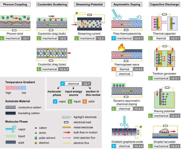
Next generation off-the-grid electronic systems call for alternative modes of energy harvesting. The past two decades has witnessed the evolution of a wide spectrum of low dimensional carbon materials with extraordinary physical and chemical properties, ideal for micro-scale electrical energy storage and generation. Tremendous progress has been made in harnessing the energy associated with the interactions between these nano-structured carbon substrates and the surrounding molecular phases, subsequently converting them into useful electricity. This review summarizes the important theoretical and experimental milestones the field has reached to date, and further classifies these energy harvesting processes based on underlying physics, into five mechanistically distinct classes – phonon coupling, Coulombic scattering, electrokinetic streaming, asymmetric doping, and capacitive discharging. With a special mechanistic focus, we hope to resolve the fundamental attributes shared by this diverse array of molecular scale energy harvesting schemes, offer perspectives on key challenges, and ultimately establish design principles that guide further device optimization.
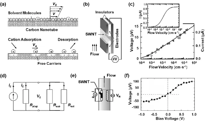
1.2.1 Motivations for Solvent Mediated Energy Harvesting Methods
There is a pressing need for alternatives to conventional energy generation techniques, due to the upper bounds on generator sizes set by the device footprint of the next generation micro- and nano-electronic systems. Recent developments in micro-fabrication techniques86-89 and understandings about low dimensional materials90-117 have culminated into some of the most exciting demonstrations of microscopic electronic platforms capable of advanced logic computations, while not being tethered to any substrates and external power supplies.2,118 These systems represent
43
a giant leap forward in combining state-of-the-art technologies in modern electrical engineering with our understandings in the chemical and biological sciences, by interfacing digital systems with traditionally prohibitive environments. With numerous engineering possibilities in areas like circulating medical diagnostic devices and remote sensors in previously inaccessible locations, the Achilles’ heel for such an electronic system at an extremely small length-scale has by and large been the energy constraint. While there has been tremendous progress towards improving the energy and power densities for traditional energy storage devices such as micro-batteries119-122 and supercapacitors123-127, their disadvantageous volumetric scaling poses fundamental constraints on
important energy metrics that limit the application space of these electricity-demanding on-board electronics.
It is for this reason that energy harvesting strategies tapping into the surrounding environments that embody and intimately interface with these microscopic platforms hold great promise for the next generation untethered micro-electronic devices. Indeed, a series of harvesting strategies, including photovoltaics,128-140 piezo-electrics,141-145 tribo-electrics,146-149 thermo-electrics,150-154 electro-magnetic transducers,155-157 fluidic electric generators,158-167 as well as bio-fuel cells168-177 have been devised in the attempt to tackle this challenge. It is worth noting, that once plugged into the environment, the energy density of such microscopic systems would no longer be limited by the device volume, for the environment can generally be treated as an infinite reservoir. Nevertheless, all the above listed harvesting strategies require a specific type of energy input, such as light, heat, mechanical movements, electro-magnetic fluctuations, or energy stored in chemical bonds; and built-in along-side this specificity are challenges associated with the intermittency of available input sources, as well as the versatility of e technology for universal implementation in various, potentially dynamic environments. Therefore, it would be ideal to develop energy