Publisher’s version / Version de l'éditeur:
Optics Express, 25, 12, pp. A530-A538, 2017-06-12
READ THESE TERMS AND CONDITIONS CAREFULLY BEFORE USING THIS WEBSITE. https://nrc-publications.canada.ca/eng/copyright
Vous avez des questions? Nous pouvons vous aider. Pour communiquer directement avec un auteur, consultez la
première page de la revue dans laquelle son article a été publié afin de trouver ses coordonnées. Si vous n’arrivez pas à les repérer, communiquez avec nous à PublicationsArchive-ArchivesPublications@nrc-cnrc.gc.ca.
Questions? Contact the NRC Publications Archive team at
PublicationsArchive-ArchivesPublications@nrc-cnrc.gc.ca. If you wish to email the authors directly, please see the first page of the publication for their contact information.
This publication could be one of several versions: author’s original, accepted manuscript or the publisher’s version. / La version de cette publication peut être l’une des suivantes : la version prépublication de l’auteur, la version acceptée du manuscrit ou la version de l’éditeur.
For the publisher’s version, please access the DOI link below./ Pour consulter la version de l’éditeur, utilisez le lien DOI ci-dessous.
https://doi.org/10.1364/OE.25.00A530
Access and use of this website and the material on it are subject to the Terms and Conditions set forth at
Procedure to decouple reflectance and down-shifting effects in
luminescent down-shifting enhanced photovoltaics
Gabr, Ahmed M.; Walker, Alexandre W.; Wilkins, Matthew M.; Kleiman,
Rafael; Hinzer, Karin
https://publications-cnrc.canada.ca/fra/droits
L’accès à ce site Web et l’utilisation de son contenu sont assujettis aux conditions présentées dans le site LISEZ CES CONDITIONS ATTENTIVEMENT AVANT D’UTILISER CE SITE WEB.
NRC Publications Record / Notice d'Archives des publications de CNRC:
https://nrc-publications.canada.ca/eng/view/object/?id=b61b8697-879c-41ed-a72d-d183ad0b44f6 https://publications-cnrc.canada.ca/fra/voir/objet/?id=b61b8697-879c-41ed-a72d-d183ad0b44f6Procedure to decouple reflectance and
down-shifting effects in luminescent down-down-shifting
enhanced photovoltaics
A
HMEDM. G
ABR,
1,*A
LEXANDREW. W
ALKER,
2M
ATTHEWM. W
ILKINS,
1R
AFAELK
LEIMAN,
3ANDK
ARINH
INZER1 1SUNLAB, University of Ottawa, 25 Templeton St., K1N 6N5, Ottawa, ON, Canada
2
National Research Council of Canada, 1200 Montreal Road, K1A 0R6, Ottawa, ON, Canada
3
Department of Engineering Physics, McMaster University, 1280 Main Street West, L8S 4L7, Hamilton, ON, Canada
*
agabr031@uottawa.ca
Abstract: The down-shifting (DS) process is a purely optical approach used to improve the short-wavelength response of a solar cell by shifting high-energy photons to the visible range, which can be more efficiently absorbed by the solar cell. In addition to the DS effect, coupling a DS layer to the top surface of a solar cell results in a change in surface reflectance. The two effects are intermixed and therefore, usually reported as a single effect. Here we propose a procedure to decouple the two effects. Analytical equations are derived to decouple the two effects, that consider the experimentally measured quantum efficiency of the solar cell with and without the DS layer, in addition to transfer matrix simulations of the parasitic absorption in the device structure. In this work, an overall degradation of 0.46 mA/cm2 is observed when adding a DS layer composed of silicon nanocrystals embedded in a quartz matrix to a silicon solar cell of 11% baseline efficiency. To fully understand the contribution from each effect, the surface reflectance and DS effects are decoupled and quantified using the described procedure. We observe an enhancement of 0.27 mA/cm2 in short-circuit current density due to the DS effect, while the surface reflectance effect leads to a degradation of 0.73 mA/cm2 in short-circuit current density.
© 2017 Optical Society of America
OCIS codes: (310.1210) Antireflection coatings; (160.2540) Fluorescent and luminescent materials; (040.5350) Photovoltaic; (040.6040) Silicon.
References and links
1. A. Luque and S. Hegedus, Handbook of Photovoltaic Science and Engineering (John Wiley & Sons, Ltd, (2010). 2. H.-C. Chen, C.-C. Lin, H.-W. Han, Y.-L. Tsai, C.-H. Chang, H.-W. Wang, M.-A. Tsai, H.-C. Kuo, and P. Yu,
“Enhanced efficiency for c-Si solar cell with nanopillar array via quantum dots layers,” Opt. Express 19(S5 Suppl 5), A1141–A1147 (2011).
3. A. Le Donne, M. Acciarri, D. Narducci, S. Marchionna, and S. Binetti, “Encapsulating Eu3+ complex doped
layers to improve Si-based solar cell efficiency,” Prog. Photovolt. Res. Appl. 17(8), 519–525 (2009). 4. Z. J. Cheng, L. K. Pan, F. F. Su, M. L. Cao, and Z. Sun, “Eu3+ doped silica film as luminescent down-shifting
layer for crystalline Si solar cells,” Surf. Rev. Lett. 16(5), 669–673 (2009).
5. H.-V. Han, C.-C. Lin, Y.-L. Tsai, H.-C. Chen, K.-J. Chen, Y.-L. Yeh, W.-Y. Lin, H.-C. Kuo, and P. Yu, “A highly efficient hybrid GaAs solar cell based on colloidal-quantum-dot-sensitization,” Sci. Rep. 4(1), 5734 (2014).
6. B. Sadeghimakki, Z. Gao, and S. Sivoththaman, “Proof of down-conversion by CdSe/ZnS quantum dots on silicon solar cells,” in Proceedings of IEEE 40th Photovoltaic Specialist Conference (PVSC, 2014), 2262–2266. 7. D. Ross, E. Klampaftis, J. Fritsche, M. Bauer, and B. S. Richards, “Increased short-circuit current density of
production line CdTe mini-module through luminescent down-shifting,” Sol. Energy Mater. Sol. Cells 103, 11– 16 (2012).
8. E. Klampaftis, D. Ross, S. Seyrling, A. N. Tiwari, and B. S. Richards, “Increase in short-wavelength response of encapsulated CIGS devices by doping the encapsulation layer with luminescent material,” Sol. Energy Mater. Sol. Cells 101, 62–67 (2012).
9. C. Cheng and J. Yang, “Hydrothermal synthesis of Eu3+ -Doped Y(OH)
3 nanotubes as downconversion materials
for efficiency enhancement of screen-printed monocrystalline silicon solar cells,” IEEE Electron Device Lett. 33(5), 697–699 (2012).
#288094 https://doi.org/10.1364/OE.25.00A530
10. E. Klampaftis, D. Ross, K. R. McIntosh, and B. S. Richards, “Enhancing the performance of solar cells via luminescent down-shifting of the incident spectrum: A review,” Sol. Energy Mater. Sol. Cells 93(8), 1182–1194 (2009).
11. A. M. Gabr, A. Walker, A. Trojnar, T. J. Hall, R. N. Kleiman, and K. Hinzer, “Numerical Modeling of Silicon Nanocrystal Down - Shifting Layers for Enhanced CIGS Solar Cell Performance,” in Proceedings of IEEE 39th
Photovoltaic Specialist Conference (PVSC, 2013), pp. 1003–1007.
12. F. Sgrignuoli, G. Paternoster, A. Marconi, P. Ingenhoven, A. Anopchenko, G. Pucker, and L. Pavesi, “Modeling of silicon nanocrystals based down-shifter for enhanced silicon solar cell performance,” J. Appl. Phys. 111(3), 34303 (2012).
13. D. Alonso-Álvarez, D. Ross, E. Klampaftis, K. R. McIntosh, S. Jia, P. Storiz, T. Stolz, and B. S. Richards, “Luminescent down-shifting experiment and modelling with multiple photovoltaic technologies,” Prog. Photovolt. Res. Appl. 23(4), 479–497 (2015).
14. W. Ding, R. Jia, D. Wu, C. Chen, H. Li, X. Liu, and T. Ye, “Numerical simulation and modeling of spectral conversion by silicon nanocrystals with multiple exciton generation,” J. Appl. Phys. 109(5), 1–7 (2011). 15. R. Rothemund, “Optical modelling of the external quantum efficiency of solar cells with luminescent
down-shifting layers,” Sol. Energy Mater. Sol. Cells 120, 616–621 (2014).
16. Z. Yuan, G. Pucker, A. Marconi, F. Sgrignuoli, A. Anopchenko, Y. Jestin, L. Ferrario, P. Bellutti, and L. Pavesi, “Silicon nanocrystals as a photoluminescence down shifter for solar cells,” Sol. Energy Mater. Sol. Cells 95(4), 1224–1227 (2011).
17. M. L. Mastronardi, F. Maier-Flaig, D. Faulkner, E. J. Henderson, C. Kübel, U. Lemmer, and G. A. Ozin, “Size-dependent absolute quantum yields for size-separated colloidally-stable silicon nanocrystals,” Nano Lett. 12(1), 337–342 (2012).
18. J. Sacks, R. Savidge, and A. Gabr, “Quantum efficiency measurements of down-shifting using silicon nanocrystals for photovoltaic applications,” in Proceedings of IEEE 38th Photovoltaic Specialist Conference (PVSC, 2012), pp. 92–96.
19. J. Sacks, Spectral Engineering via Silicon Nanocrystals Grown by ECR-PECVD for Photovoltaic Applications (McMaster University, 2012).
20. G. F. Burkhard, E. T. Hoke, and M. D. McGehee, “Accounting for interference, scattering, and electrode absorption to make accurate internal quantum efficiency measurements in organic and other thin solar cells,” Adv. Mater. 22(30), 3293–3297 (2010).
21. M. Law, M. C. Beard, S. Choi, J. M. Luther, M. C. Hanna, and A. J. Nozik, “Determining the internal quantum efficiency of PbSe nanocrystal solar cells with the aid of an optical model,” Nano Lett. 8(11), 3904–3910 (2008). 22. D. N. Micha, A. W. Walker, G. Siefer, F. Dimroth, and A. W. Bett, “Influence of a Very Efficient Back
Reflectors on the Quantum Efficiency of Solar Cells,” in Proceedings of EU-PVSEC (2016), pp. 20–24. 23. S. J. Orfanidis, “Electromagnetic Waves and Antennas,” http://www.ece.rutgers.edu/~orfanidi/ewa/. [Accessed:
08-Jan-2017].
24. D. Timmerman, J. Valenta, K. Dohnalová, W. D. A. M. de Boer, and T. Gregorkiewicz, “Step-like enhancement of luminescence quantum yield of silicon nanocrystals,” Nat. Nanotechnol. 6(11), 710–713 (2011).
25. A. M. Gabr, Modelling and Characterization of Down-Conversion and Down-Shifting Processes for
Photovoltaic Applications (University of Ottawa, 2016).
1. Introduction
Down-conversion and down-shifting optical layers mounted on the top surface of solar cells can enhance the wavelength response of single-junction solar cells. Poor short-wavelength response is either due to high surface recombination losses as in silicon solar cells, or due to parasitic absorption in window layers as in GaAs, CdTe and CIGS solar cells [1]. Down-shifting (DS) layers convert high-energy photons into lower energy photons targeted for more efficient carrier collection in the solar cell. In recent years, there have been several experimental reports of coupling DS layers to the top surface of silicon [2–4], GaAs [5, 6], CdTe [7] and CIGS [8] solar cells.
In addition to the DS effect, DS layers strongly influence the reflectivity of the front surface. When designing DS layers, one therefore considers the optical properties of the DS material such that it also acts as an anti-reflection coating (ARC). In a recent report, upon adding a DS layer to a silicon cell, the efficiency increased from 15.2% to 17.2% under AM1.5G illumination [9], an improvement of 2% absolute. However, the measured external quantum efficiency (EQE) shows an increase in the 550 – 700 nm range, which does not correspond to the absorption spectrum of the DS layer. This suggests that the improvement was dominated by reduced surface reflection of incident photons into the cell, rather than from the DS effect. In general, it is important to decouple the surface reflectance and the DS effects; otherwise the results could be misinterpreted. To quantify the contribution from each
effect, one should couple the solar cell to a non-emitting DS layer to solely account for its surface reflectance effect. Coupling the solar cell to the DS layer will then result in the total contribution, and since these two effects are linearly coupled, then the DS effect is the difference between the two experiments. This has been experimentally achieved using an undoped host material compared to a doped host material to activate the DS effect [8, 10]. However, the addition of a dopant to absorb preferentially in the short wavelength and emit at a longer wavelength will change the complex refractive index since the real and imaginary parts are related through the Kramers-Krong relations. When the dopant concentration is very small so that the change in refractive index is negligible, changes to the surface reflectance become negligible, thus allowing for a study solely on the DS effect. This procedure is proposed to rely on a modelling perspective using a DS layer with a zero photoluminescence quantum yield to account solely for reflectance effect [11, 12]. However, in other cases where the refractive index changes significantly or when a DS layer is added to the top surface, as the case in this work, there should be clear procedure to decouple the effects.
There have been a number of analytical models derived to decouple the reflectance and DS effects [5], [12–16]. However, there are some limitations in these models such as not accounting for multiple reflections and interference in thin-film layers and ignoring the effects of parasitic absorption [5, 14, 15]. These limitations can lead to an inaccurate evaluation of the DS conversion efficiency or the resulting internal quantum efficiency (IQE) of the solar cell with the DS layer, which is important in decoupling the surface reflectance and DS effects, as will be shown later.
In this work, an innovative procedure is proposed to decouple surface reflectance effect and DS effects considering the cumulative knowledge base in the research community addressing the issue. The procedure is based on measured quantum efficiency and optical modelling of parasitic absorption based on a transfer matrix method. We demonstrate the procedure by coupling a DS layer consisting of silicon nanocrystals embedded in a silicon dioxide matrix to a silicon solar cell. Silicon nanocrystals are known to absorb strongly below 500 nm with a tunable emission profile in the range of 700 nm – 900 nm based on their size [17]. While the analysis is focused on the DS process, it also applies to the more general down-conversion process where multiple low-energy photons may be re-emitted for every high-energy photon absorbed.
The paper is outlined as follows. Experimental methods in preparing the silicon solar cell and the down-shifting layer are presented in section 2, including a description of the experimental measurement setup and the measured external quantum efficiencies of the solar cell with and without the DS layer. In section 3, analytical expressions for decoupling the surface reflectance and DS effects are presented, followed by optical modelling of parasitic and active region absorption in the device. These finally lead to the individual contributions of surface reflection and DS effects to the short-circuit current density under AM1.5G spectrum. Lastly in section 4, the DS conversion efficiency of the layer is estimated based on the measured photoluminescence of the DS layer, outlining the effect of increasing the DS efficiency on the EQE of the silicon solar cell, and hence on the performance of the solar cell.
2. Experimental
2.1 Sample preparation
Silicon solar cells were fabricated at the Carleton University’s microfabrication facility. A 300 m thick p-type <100> silicon wafer was used as a substrate. The emitter was doped by phosphor diffusion using an eight-stack Bruce Model BDF-8 furnace bank. The front grid contact was made of Ti/Ag using standard photolithography techniques, while the back contact is a plane evaporated aluminum layer. Titanium Silicate was deposited by spinning on the top surface and used as an ARC. The optimum ARC thickness is 110 nm so that zero reflection is achieved at 650 nm. The ARC thickness is measured to be 115 nm using a variable angle spectroscopic ellipsometer.
Silicon nanocrystals (Si-nC) embedded in silicon dioxide matrix were grown by plasma-enhanced chemical vapor deposition (PECVD) system [18], and annealed at 1135 °C. Fused silica Spectrosil 2000 UV coverslips (CFS-2525) from UQD Optics are used as a substrate with thickness of 500 m. The Si-nC layer thickness is measured to be 484 nm thick using a variable angle spectroscopic ellipsometer. The photoluminescence (PL) of the silicon nanocrystals sample was measured, and a wide Gaussian distribution PL centered at 840 nm is observed when excited with a laser at 325 nm at room temperature [19]. The Si-nC are estimated to have an average diameter of 4 nm with average densities of 1.5 x 1011 cm−2 [19].
2.2 External quantum efficiency and reflectance measurement
The external quantum efficiency and specular reflectance were measured using a Newport IQE-200 system. The system uses a Xenon lamp as its light source. The monochromatic modulated beam is obtained using a system consisting of an Oriel 1/8 m monochromator, a chopper with a digital lock-in amplifier set at 87 Hz, order-sorting filters, and collimating lenses. The system allows measurement of EQE along with independent measurements of specular reflectance over wavelengths of 300 to 1800 nm. The detectors are calibrated using NIST traceable calibration standards.
The double layer Si-nC/SiO2 is placed on the top surface of the silicon solar cell with the
Si-nC layer directly adjacent to the solar cell, as depicted in Fig. 1(a). Since there might be airgaps due to surface roughness, a refractive index matching liquid from Cargille was used between the Si-nC and the silicon solar cell to eliminate the reflection losses associated with the Si-nC/air interface.
The EQE and reflectance were measured for the reference cell and the solar cell with the DS layer, as shown in Fig. 1(b) and (c) respectively. The poor UV response of the solar cell is due in part to parasitic absorption in the ARC layer and the high surface recombination at the silicon/ARC interface. The EQE increases gradually as the reflectance decreases with maximum EQE in the 700 nm - 800 nm range.
Figure 1(b) shows an enhancement in the EQE from 480 – 680 nm and below 400 nm due to the DS layer. A decrease in EQE is also observed in the range 400 – 480 nm, which is believed to be due to the low PLQY of the Si-nC considering the reflectivity has decreased due to the addition of the DS layer. Although the Si-nC absorb in this range (as discussed in section 3.2), the PLQY is quite low and thus only a very small fraction of the re-emitted photons reach the cell; this is discussed more in detail in section 4. However, there is degradation in the EQE at longer wavelengths (> 680 nm) mainly due to the suboptimal reflectivity after adding the DS layer (see Fig. 1(c)). When comparing surface reflectance, there is nearly 10% degradation at longer wavelengths (~1000 nm) but a strong enhancement at shorter wavelengths.
The short-circuit current density, Jsc, is computed from the measured EQE using the
relation:
( ) ( ) sc
J =q
φ λ ⋅EQE λ λd (1) where Φ( ) is the incident photon flux, and EQE( ) is the external quantum efficiency of thesolar cell. The solar cell without the DS layer (reference cell) has Jsc,ref of 26.1 mA/cm2, while
the Jsc,tot for the solar cell with DS layer is 25.6 mA/cm2 under the AM1.5G standard
spectrum (1000 W/m2). Thus an overall degradation in the short-circuit current density, ΔJsc,tot, of 0.46 mA/cm2 is observed. At this point, surface reflectance and DS effects are
intermixed and the enhancement/degradation from each effect needs to be quantified. This can be achieved by analyzing the EQE of the device combined with optical modeling.
Fig. 1. a) A schematic of silicon solar cell with a double down-shifting layer on the top surface. Measured b) EQE and c) reflectance of the solar cell with no DS layer (dashed blue line) and the solar cell with DS layer (solid red line).
3. Decoupling down-shifting and surface reflectance effects
3.1 Theory
The measured EQE of the solar cell with DS layer, denoted as EQEtot, can be linearly divided
into two components, accounting for surface reflectance and DS effects as: ( ) ( ) ( )
tot passive DS
EQE λ =EQE λ + ΔEQE λ (2) where ΔEQEDS is the change in the EQE due to the re-emission of photons from the DS layer,
accounting for the DS effect, and EQEpassive is the EQE of the solar cell with the DS layer
applied to the front surface accounting for the surface reflectance effect only. In other words, the DS layer is assumed passive with no re-emission of photons and thus acts solely as an ARC. EQEpassive can be expressed as:
( ) (1 ( ) ( )) ( )
passive tot p ref
EQE λ = −R λ −A λ ⋅IQE λ (3) where Rtot is the reflectance in the presence of DS layer, Ap is the parasitic absorption, and
IQEref refers to the IQE of the reference solar cell. Here, it is important to note that the IQE is
defined as the ratio of the number of carriers contributing to the electrical current under short-circuit to the number of photons absorbed by the active layer [20–22]. Therefore, IQE is calculated from the measured EQE as follows:
( ) ( ) ( ) pn EQE IQE A λ λ λ = (4)
where Apn( ) is the absorption strictly in the active layer of the solar cell as a function of
wavelength . This is the same equation as in Eq. (3) where Apn = 1−Rtot−AP. It is critically
important to take into account parasitic absorption when calculating IQE for structures that contain absorbing window layers, thick substrates, absorbing ARC, or in this case, DS layers.
3.2 Optical modelling
Determining the absorption in the active layer can be challenging in cases where there are other parasitically absorbing layers in the device, and usually requires optical modelling to relate experimentally measured total absorption to the absorption in each layer. The
absorption in each layer cannot be independently measured due to interference effects. Therefore, the transfer matrix method is used to calculate the relative absorption in each layer as well as interference of reflected and transmitted waves at each interface in the device [23]. This method requires knowledge of the wavelength dependent complex index of refraction of each material. The optical parameters for the ARC layer, Si-nC, and quartz substrate are measured using a variable-angle spectroscopic ellipsometer [19].
The simulated parasitic absorption is shown in Fig. 2(a) along with the measured reflectance and total absorption. The total absorption is derived from the measured reflectance assuming negligible transmission at the back of the device, i.e. A = 1−R.
Rather than using the optical model to predict the active region’s absorption, which is the main contribution to total absorption, the modeled parasitic absorption is subtracted from the experimentally measured total absorption. By subtracting the parasitic absorption from the experimentally measured data, the error due to mismatch between the optical model and the measurements is reduced.
The optical modelling for the solar cell with the DS layer is shown in Fig. 2(b). Here, the parasitic absorption includes the titanium silicate ARC absorption as well as the Si-nC layer absorption. As can be seen in Fig. 2(b), most of the short-wavelength absorption is in the Si-nC layer, with a significantly smaller absorption in the ARC. It can also be observed that it extends to longer wavelengths (>600 nm) due to the relatively thick (~500 nm) nature of the Si-nC layer, including a wide distribution of nanocrystals sizes [19]. The parasitic absorption results will be used to compute the IQE of the solar cell with and without the DS layer, as will be seen in the next section.
Fig. 2. Measured total reflectance, total absorption ( = 1-Rtot), simulated parasitic absorption and calculated absorption in the active layer as a function of wavelength of the a) reference silicon solar cell with titanium silicate as an ARC and b) a silicon solar cell with titanium silicate as an ARC coupled to Si-nC based DS layer.
3.3 Surface reflectance and DS effects
Once the parasitic absorption is accurately modeled, the EQE resulting from the reflectance effect can be decoupled using Eq. (3), and the change in the EQE due to the DS effect is thus calculated using Eq. (2). First, the contribution from the surface reflectance effect, ΔJsc,passive,
is quantified by calculating the short-circuit current density based on comparing the EQEs of the reference and passive cell as:
, ( ) ( ( ) ( )) .
sc passive passive ref
J q φ λ EQE λ EQE λ dλ
Δ =
⋅ − (5)We can then identify the DS effect by subtracting the reflectance contribution (ΔJsc,passive)
from the total contribution (ΔJsc,tot), which is the difference between the short-circuit current
density of the cell with the DS layer (Jsc.tot) and the short-circuit current density of the
reference cell (Jsc,ref). Therefore, ΔJsc,DS is calculated as:
, , ,
sc DS sc tot sc passive
J J J
Δ = Δ − Δ (6)
The calculated contribution solely due to the surface reflectance effect (ΔJsc,passive) is −0.73
mA/cm2, while the contribution due to DS effect (ΔJsc,DS) is observed to be 0.27 mA/cm2,
yielding the total degradation (ΔJsc,tot) of 0.46 mA/cm2. Decoupling the two effects gives us a
better understanding of each contribution and how the layer can be optimized. In this case, the reflectance effect dominates the degradation in the solar cell performance due to the suboptimal DS layer thickness.
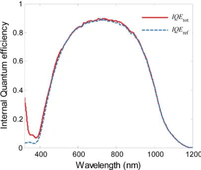
The IQE for the solar cell with the DS layer is calculated using Eq. (4) and compared to the reference IQE, as shown in Fig. 3. The IQE represents the efficiency of the active layer (i.e. the Si pn junction) in collecting photogenerated carriers, where reflection losses are excluded. Therefore, the two IQEs should be the same since the pn junction is the same. However, the difference between the two reported IQEs demonstrates the influence of the DS layer, which shifts photons from the short-wavelength region to the visible region, which is evident for < 400 nm. However, the small difference between the two curves in the 600-900 nm wavelength range is due to the non-zero absorption in the Si-nC layer, as can be seen in Fig. 2(b).
Fig. 3. Calculated IQE of the solar cell with and without the DS layer. 4. DS conversion efficiency
Once reflectance and DS effects are decoupled, the DS layer’s efficiency can be determined. The DS conversion efficiency is defined as the ratio of the number of photons that reach the underlying solar cell to the absorbed photons by the DS layer. This is not to be confused with the photoluminescence quantum yield, which is defined as the ratio of the number of emitted to the number of absorbed photons. The DS conversion efficiency consists of the
photoluminescence quantum yield of the DS layer as well as the fraction of the re-emitted photons that reach the underlying solar cell.
The conversion efficiency of the DS layer can be estimated from the measured EQE of the solar cell with the DS layer. The Si-nC emit a fraction of the absorbed photons at longer wavelengths and most of these emitted photons reach the underlying solar cell whereas a small fraction is lost through the front surface or reflected out of the cell from the DS/ARC/solar cell interfaces. The EQE describing the DS effect can be expressed as:
( ) ( ) ( ) ( )
DS DS DS ref
EQE λ A λ η PLλ′ IQE λ′dλ′
Δ = ⋅
⋅ (7)where ADS(λ) is the absorption in the DS layer, ηDS is the DS efficiency, PL(λ') is the
normalized photoluminescence of the DS layer. Substituting Eq. (7) in Eq. (2) and solving for the DS efficiency we arrive at:
( ) ( ) ( ) . ( ) ( ) ( ) tot passive DS DS ref EQE EQE A PL IQE d λ λ η λ λ λ λ λ − = ′ ⋅ ′ ′
(8)Using Eq. (8) above, the conversion efficiency is estimated to be 3% at 325 nm, which is the same excitation wavelength used in the PL experiment. This can be compared with the PLQY measurement of the same sample with an integrating sphere, spectrometer and a 405 nm solid state laser operating at approximately 16 mW, where the PLQY is measured to be 1% [19]. The difference in results could be to the different excitation wavelength, where it has been shown previously that the PLQY decreases with increasing excitation wavelength by up to a factor of three [24]. However, the difference could also be due to other cumulative errors found in this calculation such as the reflectance, EQE and PL measurements as well as the absorption simulation. Thus, the DS efficiency estimated in this section should only be used as a guiding value for the magnitude of the PLQY for a Si-nC based DS layer, and is not meant to represent an accurate measurement.
The effect of having a higher DS efficiency can be examined by increasing the efficiency in Eq. (7) while assuming the same layer thickness. Thus only the second term in Eq. (2) changes while the first term, EQEpassive, stays constant. For DS layers, the maximum
photoluminescence quantum yield is 100%. The escape cone loss for a DS layer with refractive index of 1.9, as the Si-nC in our case is 7% [25]. The upper limit for the DS efficiency thus is 93%. Figure 4(a) shows the calculated EQEs of the solar cell with DS layer with different DS efficiencies (10%, 50% and 90%). Designing DS layers with higher efficiencies enhances the short-wavelength response of the EQE and thus the short-circuit current density of the solar cell.
The short-circuit current density is computed using Eq. (1) from the simulated EQE in Fig. 4(a) to examine the effect of increasing the DS efficiency on the solar cell performance. The total change in short-circuit current density, ΔJsc.tot, is found by comparing the
short-circuit current density of the cell with a DS layer (Jsc.tot) with the short-circuit current density
of the reference cell (Jsc.ref). The total change in short circuit current density, ΔJsc.tot, is then
decoupled using the procedure proposed in section 3 to quantify the reflectance and the DS effects. The reflectance effect is assumed constant and it has an overall negative effect because of the un-optimized DS layer thickness (ΔJsc.passive = −0.73 mA/m2). Finally, the
short-circuit current density due to the DS effect (ΔJsc.DS) is calculated using Eq. (6).
The total change in the short-circuit current density and its components due to the coupling of the DS layer are shown in Fig. 4(b). The high surface reflectance results in a negative value of ΔJsc.tot, which then linearly increases as the DS efficiency increases. A DS
efficiency of 34% is required to balance the negative surface reflectance effect. For a 90% efficient DS layer, the overall enhancement is estimated to be 0.95 mA/cm2, with a 0.73 mA/cm2 loss due to reflectance effect and a 1.68 mA/cm2 gain due to the DS effect. Therefore
a 6.5% improvement to the short-circuit current density due to the DS effect yields only a 3.6% increase in total Jsc.
Fig. 4. a) Simulated external quantum efficiencies of the silicon solar cell coupled to DS layer as a function of DS efficiency. The measured EQE (dotted black) of the solar cell with DS layer is also shown for comparison. b) Calculated normalized short-circuit current densities components as a function of DS efficiency.
5. Conclusion
In conclusion, we have presented a procedure to decouple the surface reflectance effect and the down-shifting (DS) effect. The procedure involves measuring the external quantum efficiency and surface reflectance of the solar cell with and without the DS layer, and in parallel, performing optical modelling to calculate the optical absorption in each layer of the device. We demonstrate the procedure using a DS layer composed of silicon nanocrystals embedded in a quartz matrix and coupled to a monocrystalline silicon solar cell. Results show that an overall degradation in short-circuit current density of 0.46 mA/cm2 occurs when adding the DS layer. The surface reflectance alone results in a degradation of 0.73 mA/cm2, whereas the DS effect results in a small enhancement of 0.27 mA/cm2. The proposed procedure also allows for extracting the DS efficiency, which in this case is 3%. The model thus suggests that a DS efficiency of 34% would be required to negate the degradation arising from the DS’s suboptimal ARC properties. This demonstrates a systematic approach of decoupling reflectance and DS effects, which can be applied to any solar cell with down-conversion or down-shifting layers when the optical properties of the complete stack are known. Adopting this procedure would help to clarify many of the results that are published on down-shifting and down conversion processes.
Funding
Natural Sciences and Engineering Research Council of Canada (NSERC) (501100000038).
Acknowledgments
The authors would like to thank Dr. Garry Tarr from Carleton University for providing the silicon solar cell used in this work and Kevin Boyd from McMaster University for measuring the optical properties of the ARC layer.