SUPPORTING INFORMATION
Reduced ensemble plasmon linewidths and enhanced
two-photon luminescence in anodically formed high surface
area Au-TiO
23D nanocomposites
Samira Farsinezhad,
1Shyama Prasad Banerjee,
1Bharath Bangalore Rajeeva,
1Benjamin D. Wiltshire,
1Himani Sharma,
1Anton Sura,
1Arash
Mohammadpour,
1Piyush Kar,
1Robert Fedosejevs
1and Karthik Shankar
1, 2*
1
Department of Electrical and Computer Engineering, University of Alberta, 9107 - 116 St, Edmonton, Alberta, Canada T6G2 V4.
2
NRC National Institute for Nanotechnology, 11421 Saskatchewan Dr NW, Edmonton, AB T6G 2M9.
Corresponding Author
* Address: Prof. Karthik Shankar, Department of Electrical & Computer Engineering, University of Alberta, Edmonton, AB, Canada. Email: kshankar@ualberta.ca
EXPERIMENTAL DETAILS
Synthesis of A-PLATENsTwo types of substrates were used in all experiments, named borosilicate glass slides (Corning Inc.) and fluorine-doped tin oxide (FTO)-coated glass substrates (Hartford Glass Co.). The substrates were cleaned by sonication in soap, water, methanol and acetone and subsequently loaded into a DC magnetron sputtering system (Kurt J. Lesker Co.). Two separate targets of Ti and Au were used to vacuum deposit the TiAu thin film stack. The power applied during sputtering to the Au target was 1-3 W and that to the Ti target was 150 W keeping in mind that the sputter yield of Ti is roughly one-fifth that of Au for the Argon ion energies typically used in sputtering.1 When purely co-sputtered films with gold concentration higher than 1 % are formed without alternation with Ti layers, the etching process was uneven and resulted in un-anodized areas on the substrate. Stirring improved the uniformity of the anodized films and also decreased the anodization duration from ~40 minutes to ~ 10 minutes. Consequently, stirring was employed throughout for all anodic processes related to the TiAu composite films. We experimented with a number of co-sputtered films as well as alternating layers until we achieved optimal results with the thin film stack depicted in shown in Fig. 1b in the main manuscript with a total thickness of 500 nm. The first layer in this stack always consisted of a Ti layer directly deposited on to the substrate in order to ensure an adherent and compact barrier layer of TiO2. A regular Ti film of identical thickness was sputtered on
to the substrate and served as the control sample. The anodization was performed potentiostatically at room temperature using voltages from 40-80 V in ethylene glycol-based electrolytes containing 0.5-5 % water and 0.1-0.5 % NH4F with a graphite counter
electrode. Both the ethylene glycol and NH4F were of ACS grade and procured from
Fisher Scientific Inc. Subsequent to anodization, debris on the top surface of the anodized films was removed by a short reactive ion etch in a SF6 plasma. 50 % of all fabricated
samples were subjected to thermal annealing in a Lindberg Blue-M three-zone tube furnace to induce crystallinity; other samples were left in the as-anodized state. The annealing regimen consisted of a 2 hour dwell at 450 °C in air and 2 hour ramp-up and ramp-down times.
Characterization
Field emission scanning electron microscopy was performed using a Hitachi S-4800 instrument operating at 5 kV accelerating voltage. A JEOL 2200FS instrument operating at 200 kV was used to obtain the transmission electron micrographs and selected area electron diffraction and fringe patterns. Raman spectra were obtained using 780 nm laser excitation in a Thermo Nicolet Almega confocal Raman microscope and spectrometer. UV-Vis spectra were collected in a Perkin-Elmer Lambda 1050 UV–Vis–NIR spectrophotometer equipped with a 150 mm integrating sphere to measure total diffuse reflectance. X-ray diffractograms were measured at grazing incidence using a Bruker D8 Discover system with a sealed Cu tube X-ray source. Confocal fluorescence micrographs were obtained in a Zeiss LSM 510 NLO multi-photon microscope using 800 nm excitation from a Ti:sapphire laser.
FDTD Simulations
OptiFDTD 8.0 (Optiwave, Inc.) was used for simulation of Au NP-decorated TiO2
nanotubes. The optical investigation was performed in the wavelength range from 400 nm to 800 nm in which the complex refractive indices of Au and TiO2 were defined
through the Lorentz-Drude model. The values of the complex permittivity of Au were taken from the Handbook of Palik2 while the parameters used for TiO2 were previously
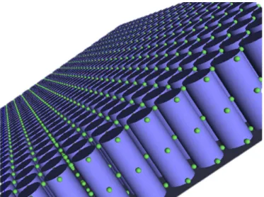
reported elsewhere by us.3 The architecture simulated was one consisting of 300 nm length nanotubes with a pore size of 80 nm and the wall thickness of 30 nm which were standing onto a barrier layer with the thickness of 50 nm. We considered 30x30 nanotubes organized adjacent to each other in a hexagonal lattice in the x-y plane and oriented in the z-direction. Au nanoparticles sized 10 nm, 20 nm and 40 nm were placed in-between adjacent nanotubes as shown in Fig. S1. A x-polarized Gaussian beam with the bandwidth of was illuminating the sample in z-direction. Anisotropic perfectly matched layer (APML) was imposed as the boundary condition. The results of this simulation are shown in Fig. 4d in the main manuscript while the geometric model used is shown in Fig. S1. A non-linear mesh with a minimum mesh size of 2.5 nm as used and each simulation was run for 5000 seconds. Spatial visualizations of the local electric field intensities were extracted at desired wavelengths. The obtained transmission is qualitatively similar to the empirical transmittance data of transparent nanotube arrays of similar dimensions consisting of a broad peak in the short wavelength region, a trough in the mid-wavelength region and gently rising for longer wavelengths.
Fig. S1. Model of TiO2 nanotubes decorated with gold nanoparticles used in FDTD
simulations.
Two-photon spectroscopy and imaging
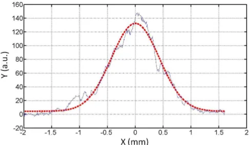
The experimental setup used for this experiment is shown in Fig. 5a in the main manuscript. A Ti:Sapphire (Spectra-Physics Hurricane) laser was used for our study to generate ~ 120 fs (FWHM, assuming a Gaussian pulse shape) pulses at 800 nm with the maximum energy ~ 600 µJ. We used a half-wave plate and a Glan polarizer to control the output laser pulse energy. We used one positive and one negative lens to modify the input laser beam. The spot size at the target surface is shown in Fig. S2. The spot diameter is 1.83 mm (1/e2 intensity diameter).
Fig. S2. Laser spot at the sample
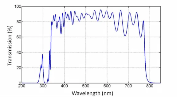
Energy delivered to the sample was calibrated using a photodiode cross calibrated against a Spectra Physics model 407A power meter and monitored for every setting of pulse energy in the experiments. The emission light was collected by an f/4 off-axis parabolic mirror and imaged onto the entrance slit of the spectrometer (MS260i) with another parabolic mirror. Two 800 nm, 0omirrors were placed in the path of the emission light to remove any contribution from the 800 nm laser pulse. Transmission of 185 – 850 nm light through the 800 nm, 0omirror is shown in Fig. 3. It shows that the transmission of light in the range of 350 – 750 nm is ~ 70%. A grating with 150 lines mm−1 and 1 mm wide entrance slit were used for the experiments reported. Spectra were recorded using a gated intensified CCD camera (Andor iStar ICCD). The targets were mounted in a precision micro-positioning linear translation stage perpendicular to the laser axis. The gate delay time was optimized within 1 nanosecond of the laser pulse. 1000 ns gate width was taken for this experiment. The peak laser energy fluence was calculated using ⱷ = 2E/πr2, whereⱷ is the energy fluence, E is the laser pulse energy and r is the radius of the ablation spot (1/e2). 100 μJ laser pulse energy corresponds to 7.64 mJ/cm2.
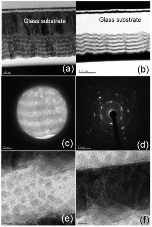
Fig. S4. Transmission electron micrographs (TEM) of the vacuum deposited multilayer
thin film stack used to form A-PLATENs (a) bright field image of the stack (b) high angle annular dark field (HAADF) image of the stack (c) TEM of the region from which the selected area electron diffraction (SAED) pattern shown in (d) is collected (e) and (f) HRTEM lattice fringe patterns
Fig. S5. Peak decomposed 2-photon PL spectra for A-PLATENs before annealing (a)
and after annealing (b), compared with the corresponding spectra of anodic TiO2
nanotubes decorated by gold nanoparticles formed by more conventional methods such as (c) vacuum deposition followed by thermal dewetting and (d) soaking in chloroauric acid followed by pyrolysis.
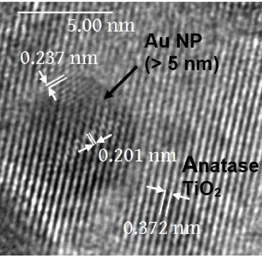
Fig. S6. Post-annealing HRTEM fringe patterns showing more than one facet, i.e. Au
(111) and Au (200), characterized by 0.237 nm and 0.201 nm lattice distances, respectively. The nanoparticle is larger than 5 nm, and is embedded within the anatase TiO2lattice.
Fig. S7. HRTEM image of a small (i.e. ~5 nm) Au NP within the anatase TiO2 lattice.
The existence of coherent heterointerface between the Au NP and anatase TiO2 lattice
can be observed.
REFERENCES
(1) Laegreid, N.; Wehner, G. K. Sputtering Yields of Metals for Ar+ and Ne+ Ions with Energies from 50 to 600 eV. J. Appl. Phys. 1961, 32, 365-369.
(2) Lynch, D. W.; Hunter, W. R., Comments on the Optical Constants of Metals and an Introduction to the Data for Several Metals A2 - Palik, Edward D. In Handbook of
Optical Constants of Solids, Academic Press: Burlington, 1997; pp 275-367.
(3) Mohammadpour, A.; Shankar, K. Anodic TiO2 Nanotube Arrays with Optical Wavelength-Sized Apertures. Journal of Materials Chemistry 2010, 20, 8474-8477.