Publisher’s version / Version de l'éditeur:
Vous avez des questions? Nous pouvons vous aider. Pour communiquer directement avec un auteur, consultez la
première page de la revue dans laquelle son article a été publié afin de trouver ses coordonnées. Si vous n’arrivez pas à les repérer, communiquez avec nous à [email protected].
Questions? Contact the NRC Publications Archive team at
[email protected]. If you wish to email the authors directly, please see the first page of the publication for their contact information.
https://publications-cnrc.canada.ca/fra/droits
L’accès à ce site Web et l’utilisation de son contenu sont assujettis aux conditions présentées dans le site LISEZ CES CONDITIONS ATTENTIVEMENT AVANT D’UTILISER CE SITE WEB.
Nano Letters, 15, 8, pp. 5131-5136, 2015-08-12
READ THESE TERMS AND CONDITIONS CAREFULLY BEFORE USING THIS WEBSITE.
https://nrc-publications.canada.ca/eng/copyright
NRC Publications Archive Record / Notice des Archives des publications du CNRC :
https://nrc-publications.canada.ca/eng/view/object/?id=65852c4c-ce37-4aff-a42f-101c402dccf7 https://publications-cnrc.canada.ca/fra/voir/objet/?id=65852c4c-ce37-4aff-a42f-101c402dccf7
NRC Publications Archive
Archives des publications du CNRC
This publication could be one of several versions: author’s original, accepted manuscript or the publisher’s version. / La version de cette publication peut être l’une des suivantes : la version prépublication de l’auteur, la version acceptée du manuscrit ou la version de l’éditeur.
For the publisher’s version, please access the DOI link below./ Pour consulter la version de l’éditeur, utilisez le lien DOI ci-dessous.
https://doi.org/10.1021/acs.nanolett.5b01346
Access and use of this website and the material on it are subject to the Terms and Conditions set forth at
High-Q/V monolithic diamond microdisks fabricated with
quasi-isotropic etching
High‑Q/V Monolithic Diamond Microdisks Fabricated with
Quasi-isotropic Etching
Behzad Khanaliloo,
†,‡Matthew Mitchell,
†,‡Aaron C. Hryciw,
‡,§and Paul E. Barclay*
,†,‡†
Department of Physics and Astronomy and Institute for Quantum Science and Technology, University of Calgary, Calgary, AB T2N 1N4, Canada
‡
National Institute for Nanotechnology, 11421 Saskatchewan Drive Northwest, Edmonton, AB T6G 2M9, Canada §
nanoFAB Facility, University of Alberta, Edmonton, AB T6G 2R3, Canada
ABSTRACT: Optical microcavities enhance light−matter interactions and are essential for many experiments in solid state quantum optics, optomechanics, and nonlinear optics. Single crystal diamond microcavities are particularly sought after for applications involving diamond quantum emitters, such as nitrogen vacancy centers, and for experiments that benefit from diamond’s excellent optical and mechanical properties. Light−matter coupling rates in experiments involving microcavities typically scale with Q/V, where Q
and V are the microcavity quality-factor and mode-volume, respectively. Here we demonstrate that microdisk whispering gallery mode cavities with high Q/V can be fabricated directly from bulk single crystal diamond. By using a quasi-isotropic oxygen plasma to etch along diamond crystal planes and undercut passivated diamond structures, we create monolithic diamond microdisks. Fiber taper based measurements show that these devices support TE- and TM-like optical modes with Q > 1.1 × 10⁵
and V < 11(λ/n)3at a wavelength of 1.5 μm.
KEYWORDS: Diamond, microcavity, nanophotonics, nanofabrication, microdisk
S
ingle-crystal diamond is a desirable material for quantum and nonlinear nanophotonics applications owing to its large electronic bandgap and correspondingly broad optical transparency window, its relatively high refractive index, and its ability to host optically active color center spins.1 Diamond’s low multiphoton absorption and thermal stability amid high optical intensities can be harnessed for nonlinear effects including Raman lasing2 and parametric down-conversion.3 Diamond also possesses exceptional mechanical properties, such as a high Young’s modulus and low intrinsic mechanical dissipation,4,5which in combination with its ability to support high optical field intensities, make diamond a promising platform for cavity-optomechanics experiments.6The excellent coherence properties of electronic and nuclear spins associated with diamond color centers have enabled a wide range of quantum optics and quantum information processing applica-tions including storing and manipulating quantum informa-tion,7−12 generating single photons,13,14and creating entangle-ment.15,16 High quality-factor (Q), small mode-volume (V) optical microcavities, which increase the rate of light−matter interactions via a local density of states ∝Q and per-photon intensity ∝1/V, enhance many physical processes underlying these applications.17−20 Microdisk-based microcavities have proven to be particularly effective, enabling experiments such as single-photon generation,21strong coupling between photons and quantum emitters,22,23 and sideband resolved optome-chanics.24−26Here we demonstrate microdisks fabricated from single crystal diamond that support optical modes with Q > 1.1×10⁵and V < 11(λ/n)3, providing a promising platform for future diamond-based applications requiring high Q/V optical resonances.
Fabrication of nanophotonic devices from single crystal diamond is challenging owing to the wavelength-scale vertical and in-plane refractive index contrast required for optical confinement. Microdisk fabrication typically involves patterning devices from thin films supported by a substrate that can be undercut, leaving a microdisk supported by a pedestal. These devices support whispering gallery modes confined to the outer perimeter of the microdisk by refractive index contrast in the radial and vertical directions.22,23 Fabricating devices with the necessary vertical confinement in single crystal diamond has relied on patterning thin single crystal diamond films created using wafer bonding3,18,27,28 or liftoff,27 and on hybrid material20,29,30 approaches. However, the ability to create microcavities directly from bulk-diamond chips is desirable. Successful bulk-diamond fabrication approaches demonstrated prior to this work include focused ion-beam milling31,32 and Faraday cage angled plasma etching.33,34
The approach demonstrated here, outlined in Figure 1, panel a and inspired by the SCREAM technique for creating structures from single crystal silicon,35 defines monolithic microdisks such as those shown in Figure 1, panels b and c
Received: April 7, 2015 Revised: June 25, 2015 Published: July 2, 2015 Letter pubs.acs.org/NanoLett 5131
from bulk diamond. This scalable technique relies upon undercutting of diamond with inductively coupled plasma reactive-ion etching (ICPRIE) along diamond crystal planes using a zero bias oxygen plasma.36This approach, which was also recently used to create diamond nanobeams,36shares the low material damage characteristics of the Faraday cage ICPRIE process of Burek et al.33 while providing an undercut profile intrinsic to the device geometry and etching parameters. It is fully compatible with standard nanofabrication tools and does not require modification to the etching tool setup.
The high-Q/V single crystal diamond microdisks studied here were fabricated as follows. A ⟨ 100 ⟩−oriented optical-grade single crystal diamond chip (3 mm × 3 mm × 0.3 mm) grown using chemical vapor deposition (Element Six) was mechanically polished (Delaware Diamond Knives), cleaned in boiling piranha (3:1 H2SO4:H2O2), and coated with a 400
nm-thick layer of PECVD silicon nitride (Si3N4) (Figure 1a(i)).
Microdisks were patterned using electron-beam lithography (EBL) with ZEP520A resist. The EBL resist was developed in ZED-N50 at low temperature (−15 °C) to minimize sidewall roughness (Figure 1a(ii)). To prevent charging during EBL, the sample was coated with ∼5 nm of titanium (Ti) via electron-beam evaporation after the Si3N4 deposition. Alternatively,
coating the EBL resist with a water-soluble conductive polymer (aquaSAVE) was found to be effective.
The resist pattern was transferred to the Si3N4 hard mask
using an ICPRIE etch with C4F8/SF6chemistry (Figure 1a(iii)).
All ICPRIE steps were performed using an Oxford Instruments PlasmaLab 100 etcher. The exposed Ti layer was also removed by the Si3N4etch. Following the etch, the remaining resist was
stripped off using a 10 min deep-UV exposure (1.24 mW/cm2,
254 nm wavelength) and a 5 min soak in Remover PG at 70 °C. The pattern was transferred to the diamond using an anisotropic O2 ICPRIE etch (RF power 80 W, ICP power
850 W) with high diamond-to-Si3N4 etch selectivity (40:1)
(Figure 1a(iv)). This etch is characterized by a high diamond etch rate (60 nm/min), smooth and vertical diamond sidewalls, and no observed micromasking. The etch time was determined by the desired final device thickness. Next, the vertical sidewalls were protected using a conformal coating of ∼200 nm PECVD Si3N4 (Figure 1a(v)) followed by an anisotropic C4F8/SF6
ICPRIE etch to remove the Si3N4from patterned nonsidewall
surfaces such as the bottoms of the windows surrounding the microdisks (Figure 1a(vi)). During this step, it is crucial not to overetch the Si3N4 protection layer to ensure that the top
corners of the vertical sidewalls remain coated with Si3N4. The
patterned structures were then undercut using a quasi-isotropic O2 ICPRIE etch with zero preferential ion directionality
(Figure 1a(vii)). This etch employs no vertical ion plasma acceleration (zero RF power), a dense plasma (3000 W ICP power and a chamber pressure of 15 mTorr), and an elevated sample temperature (250 °C). Finally, as shown in Figure 1, panel a(viii), the Si3N4 and Ti layers were removed by
wet-etching in 49% HF followed by cleaning in boiling piranha. The quasi−isotropic undercut etch step is critical for creating microdisk devices and prior to this work has not been reported for microcavity fabrication. Of particular importance for creating high-Q whispering-gallery mode cavities is that the fabrication process creates a pedestal sufficiently isolated from the whispering gallery modes to prevent radiation loss into the substrate and a microdisk bottom surface free of features, which break the azimuthal symmetry. As illustrated schematically in
Figure 1.(a) Schematic of the microdisk fabrication process steps. (i) Polished bulk single crystal diamond chips are cleaned in boiling piranha and coated with a 400 nm thick PECVD Si3N4layer, coated with a thin (∼5 nm) Ti anticharging layer, and EBL resist (ZEP 520A). (ii) Microdisks are
patterned in ZEP using EBL and developed in ZED−N50. (iii) Patterns are transferred to the Si3N4 hard mask using an ICPRIE etch. ZEP is
removed using a deep-UV exposure and Remover PG. (iv) Patterns are transferred to the diamond using an anisotropic O2plasma ICPRIE etch. (v)
The diamond sidewalls are protected with a conformal coating of PECVD Si3N4. (vi) A short ICPRIE etch removes Si3N4from the bottom of the
etch windows. (vii) A zero bias O2ICPRIE plasma undercuts the microdisks by etching along crystal planes. (viii) The sample is soaked in HF to
remove the remaining Si3N4layer, followed by a piranha clean. (b) A 45° rotated scanning electron microscope (SEM) image of a 7.9 μm diameter
microdisk in a diamond chip with ⟨ 100 ⟩−oriented surface and edge crystal planes. (c) Overview of an array of fabricated microdisks.
Nano Letters Letter
DOI: 10.1021/acs.nanolett.5b01346 Nano Lett.2015, 15, 5131−5136
Figure 2, panel a, and visible in the SEM images of fabricated devices in Figure 1, panels b and c, the quasi-isotropic undercut was observed to etch in directions defined by clearly visible diamond crystal planes. This behavior is consistent with the etch being dominantly chemical in nature and is commonly observed in wet etching of crystalline materials such as silicon. Figure 1, panel b identifies the { 100 } and { 111 } families of crystal planes along which the undercut of the unpatterned region surrounding the microdisk is observed to proceed. Etching along the { 100 } planes is horizontal or vertical, while etching along the { 111 } planes is at a 35.26° angle with respect to the diamond surface. The microdisk pillar is etched along similar families of crystal planes, which intersect as the pillar diameter is reduced. As indicated in Figure 2, panel d, purely vertical and horizontal etching along the { 100 } planes will result in a square microdisk pedestal and reduced microdisk thickness, respectively. Etching along the { 111 } planes defines surfaces at a 35.26° angle with respect to the sample surface. The resulting quasi-isotropic undercut etch creates an hourglass-shaped pedestal supporting a microdisk. The micro-disk thickness was observed to vary by ±10%, measured from SEM images, where the thickest (thinnest) parts are aligned with the { 111 } ({ 100 }) families of crystal planes (Figure 2e). Figure 3, panel a shows the effect of microdisk diameter on the observed upward, minor inward, and major inward undercut etch distances, as defined in the Figure 3, panel a inset, for two sets of microdisks with different anisotropic and
quasi-isotropic etch times. Etch distances were measured directly from SEM images. A small variation (<100 nm) in microdisk thickness was observed as a function of increasing microdisk diameter, resulting from smaller diamond microdisks requiring less undercut time before etching along the { 100 } and { 111 } families of crystal planes intersect. We have not observed any variation in etch properties across the chip area. In some cases, the microdisk pedestals are slightly misaligned with the microdisk center. Devices exhibiting this feature typically have windows that were not completely cleared during the anisotropic etching step, which in turn locally affects the undercut etch step.
The nonlinear nature of the undercut etch rates is shown in Figure 3, panel b, which gives etch distance as a function of etch time. The upward etch rate, which together with the initial anisotropic etch depth defines the microdisk thickness, is observed to vary quadratically with the undercut etch time. The minor inward etch distance, which defines the pedestal base size, has a similar etch time dependence. This is consistent with the minor inward etch distance and thickness being defined by the ((100), (1̅00), (010), (01̅0)), and (001) planes, respectively. The major inward etch distance increases approximately twice as fast as the upward and minor inward etch rates, which can be explained by the fact that the pedestal waist is etched simultaneously along both the { 100 } and { 111} families of crystal planes. It is expected that the inward etch rates can be increased by introducing a second diamond
Figure 2.(a) Illustration of the observed undercut etching processes. Etching along the { 100 } and { 111 } families of crystal planes is shown by black and red arrows, respectively. The left (right) image shows a right angle (45° rotated) view of the microdisk cross-section. (b) Tilted (60°) SEM image shows the (010) and { 111 } planes, marked in black and red, respectively. The { 111 } planes have an angle of θ = 35.26° with respect to the diamond surface. (c) Top-down SEM image of the microdisk and windows showing the amount of undercut along the crystal directions. (d) SEM image illustrating how the octagon-shaped pedestal results from etching along { 100 } and { 111 } crystal planes. (e) A 60° tilted image of a broken and flipped microdisk.
Nano Letters Letter
anisotropic etch step after step vi in Figure 1, panel a, as in the SCREAM process.35
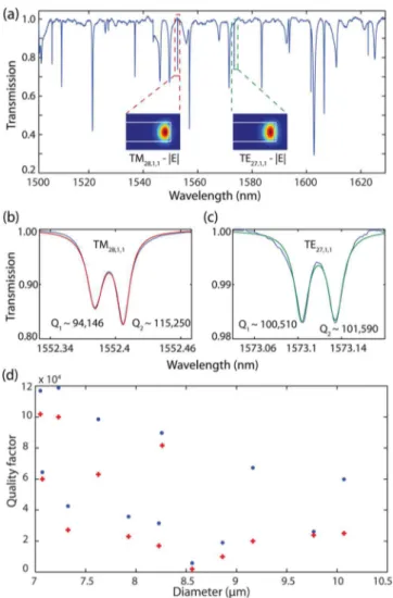
Microdisk optical cavities require small pedestal size and wavelength scale thickness to support high-Q optical modes. Here, microdisk cavities were fabricated using a 35 min (∼2 μm deep) anisotropic etch followed by a 11 h quasi-isotropic etch to undercut the devices. The optical properties of the microdisks were measured by monitoring the wavelength-dependent transmission of a tunable diode laser (Santec TSL-510, wavelength range of 1500−1630 nm) through a dimpled optical fiber taper37evanescently coupled to the microdisk. A typical normalized transmission spectra for a ∼ 7.0 μm diameter microdisk with a thickness of ∼1.0 μm and pillar base diameter of ∼4.6 μm is shown in Figure 4, panel a. This spectra contains many resonances corresponding to high-Q whispering-gallery modes of the microdisk, including high-Q TE- and TM-like modes, and modes that are higher-order in the radial and vertical directions. The highest-Q resonance observed in this microdisk is shown in Figure 4, panel b, and has loaded Qt≈ 1.09 × 10⁵and intrinsic Qi≈ 1.15 × 10⁵, where
1/Qt= 1/Qi+ 1/Qf, and Qfaccounts for the loading by the fiber
taper coupling.38This is comparable to the highest reported Q measured in single crystal microcavities to date.3,34 By using this technique, smaller microdisks optimized to support modes in the ∼637 nm wavelength range resonant with diamond nitrogen vacancy color centers can be fabricated. These devices will require shorter anisotropic (∼10 min) and isotropic (∼6 h) etch times and fabrication of smaller diameter dimpled optical fiber tapers.25,34
By comparing measured Qi and mode wavelength spacing values with the mode spectrum predicted from finite-difference-time-domain (FDTD) simulations39and measuring the polar-ization dependence of the resonance contrast, this resonance is identified as the fundamental TM-like mode. The predicted modal indices are [m,n,q] = [28,1,1], which describe the mode’s azimuthal (m), radial (n), and vertical (q) order. The resonance corresponding to the fundamental TE-like mode is shown in Figure 4, panel c, with Qi≈ 1.02 × 10⁵and modal indices of [27,1,1]. The doublet structure of the resonances in Figure 4, panels b and c is the result of backscattering and indicates that the resonances correspond to standing wave modes.40 The
Figure 3. (a) Undercut etch distance as a function of microdisk diameter. The upward, major inward, and minor inward etch distances, as defined in the inset, are shown for chip 1 (2) with ∼24 (15) minutes of anisotropic and ∼10 (7) hours of isotropic etch times with solid (dashed) lines as a guide for eye. Inset: schematic showing definition of upward, major inward, and minor inward etch distances. (b) Etch distance as a function of undercut etch time for a 7 μm microdisk, extracted by comparing chips 1 and 2. Solid lines are t2(t:
time) fits to the data.
Figure 4.(a) Normalized transmission spectra of an optical fiber taper evanescently coupled to a single crystal diamond microdisk with diameter ∼7.0 μm and thickness ∼1.0 μm. Fundamental TE-like and TM-like modes and the associated electric field profiles are highlighted. (b,c) Narrow-range wavelength scan of a high-Q TM-like (TE-TM-like) mode with [m,n,q] = [28,1,1]([27,1,1]) mode indices, respectively. (d) Highest and second highest quality factors for different microdisk diameters are shown by blue dots and red crosses, respectively.
Nano Letters Letter
DOI: 10.1021/acs.nanolett.5b01346 Nano Lett.2015, 15, 5131−5136
FDTD calculated field profiles of these modes are shown in Figure 4, panel a, and are found to have standing-wave mode volume VTM= 10.7 (λ/nd)3and VTE≈ 12.6 (λ/nd)3, as defined
by the maximum electric field strength. These mode volumes are approximately an order of magnitude smaller than those of comparable high-Q whispering gallery mode microcavities.34
Insight into the mechanism limiting Q of these devices is provided by the FDTD simulations and the observed Q dependence on microdisk diameter. Simulations of the idealized microdisk geometry studied here, which assumes perfect azimuthal symmetry for the pedestal, predict Q > 107
for both the fundamental TE- and TM-like modes, indicating that radiation loss and leakage into the substrate via the pedestal does not limit the Q of these devices. However, the noncylindrical pedestal shape created by the undercut etch can significantly affect optical loss in the microdisk by breaking the azimuthal microdisk symmetry and creating scattering not accounted for in the FDTD simulations performed here. The microdisk studied in Figure 4, panel a is the smallest diameter device on the chip and supports modes with Q comparable to the highest observed among of the tested devices. As shown in Figure 4, panel d, Q was observed to decrease with increasing microdisk diameter. This behavior contradicts expectations that
Q should increase in larger microdisks due to stronger optical
confinement.40,41 However, this behavior is consistent with interactions between the whispering gallery modes and the noncylindrical pedestal limiting Q: as the microdisk diameter increases, the noncylindrical pedestal extends closer to the microdisk perimeter, and its influence on Q increases. Moreover, the similar quality factors of the TE-like and TM-like modes indicate that scattering loss from the top or side surface is not the dominant sources of loss.41−43 Loss from interaction with the pedestal can be reduced by increasing the relative undercut either through fabrication of smaller diameter microdisks or using a longer undercut etch. It is expected that the addition of the previously mentioned second anisotropic diamond etch will reduce this effect by increasing the horizontal undercut rate.35Finally, surface roughness also affects the Q of these devices and may be reduced through improved cleaning and use of reflow techniques.41
To maximize the enhancement provided by these devices for nonlinear, quantum, and optomechanical effects, further optimization of the fabrication process is possible. It is expected that increases to Q/V are attainable by reducing the pedestal diameter and investigation of diamond cleaning and annealing recipes that may allow improvements in surface quality of the devices.31,44 Smaller pedestals are also desirable for reducing the dissipation of microdisk mechanical resonances used in optomechanics experiments.45,46 Although this fabrication process has been shown to allow creation of high mechanical quality factor nanobeam structures,36 it is expected that the relatively large pedestal diameter will limit the mechanical dissipation properties of the microdisk mechanical resonan-ces.47 Reducing the relative pedestal size to minimize mechanical dissipation26 can be achieved through longer undercut etch times or by studying smaller microdisks operating at shorter wavelengths. Additional anisotropic etch steps may provide additional means for tailoring the pedestal profile.
Reduction of the microdisk diameter and thickness, and as a result V, is desirable to enhance processes involving light matter coupling and is possible without reducing Q for sufficiently small pedestals. Given the high Q/V of the devices measured
here, it is expected that they will enable future experiments in high-frequency cavity optomechanics,25 and with further optimization to minimize V while operating at visible wavelengths, will allow enhanced optical coupling to diamond color centers.18,30
■
AUTHOR INFORMATIONCorresponding Author
*E-mail: [email protected].
Notes
The authors declare no competing financial interest.
■
ACKNOWLEDGMENTSThis work was supported by NRC, CFI, iCORE/AITF, and NSERC.
■
REFERENCES(1) Aharonovich, I.; Greentree, A. D.; Prawer, S. Nat. Photonics 2011, 5, 397−405.
(2) Spence, D. J.; Granados, E.; Mildren, R. P. Opt. Lett. 2010, 35, 556−558.
(3) Hausmann, B. J.; Bulu, I.; Venkataraman, V.; Deotare, P.; Lončar, M. Nat. Photonics 2014, 8, 369−374.
(4) Burek, M. J.; Ramos, D.; Patel, P.; Frank, I. W.; Lončar, M. Appl. Phys. Lett. 2013, 103, 131904.
(5) Aharonovich, I.; Neu, E. arXiv:1408.5451 [quant-ph] 2014. (6) Aspelmeyer, M.; Kippenberg, T. J.; Marquardt, F. Rev. Mod. Phys. 2014, 86, 1391−1452.
(7) Wrachtrup, J.; Jelezko, F. J. Phys.: Condens. Matter 2006, 18, S807−S824.
(8) Maurer, P. C.; Kucsko, G.; Latta, C.; Jiang, L.; Yao, N. Y.; Bennett, S. D.; Pastawski, F.; Hunger, D.; Chisholm, N.; Markham, M.; Twitchen, D. J.; Cirac, J. I.; Lukin, M. D. Science 2012, 336, 1283− 1286.
(9) Jelezko, F.; Gaebel, T.; Popa, I.; Domhan, M.; Gruber, A.; Wrachtrup, J. Phys. Rev. Lett. 2004, 93, 130501.
(10) Jelezko, F.; Gaebel, T.; Popa, I.; Gruber, A.; Wrachtrup, J. Phys. Rev. Lett. 2004, 92, 076401.
(11) Dutt, M. V. G.; Childress, L.; Jiang, L.; Togan, E.; Maze, J.; Jelezko, F.; Zibrov, A. S.; Hemmer, P. R.; Lukin, M. D. Science 2007, 316, 1312−1316.
(12) Heshami, K.; Santori, C.; Khanaliloo, B.; Healey, C.; Acosta, V. M.; Barclay, P. E.; Simon, C. Phys. Rev. A: At., Mol., Opt. Phys. 2014, 89, 040301(R).
(13) Sipahigil, A.; Jahnke, K.; Rogers, L.; Teraji, T.; Isoya, J.; Zibrov, A.; Jelezko, F.; Lukin, M. Phys. Rev. Lett. 2014, 113, 113602.
(14) Kurtsiefer, C.; Mayer, S.; Zarda, P.; Weinfurter, H. Phys. Rev. Lett. 2000, 85, 290.
(15) Bernien, H.; Hensen, B.; Pfaff, W.; Koolstra, G.; Blok, M. S.; Robledo, L.; Taminiau, T. H.; Markham, M.; Twitchen, D. J.; Childress, L.; Hanson, R. Nature 2013, 497, 86−90.
(16) Togan, E.; Chu, Y.; Trifonov, A. S.; Jiang, L.; Maze, J.; Childress, L.; Dutt, M. V. G.; Sørensen, A. S.; Hemmer, P. R.; Zibrov, A. S.; Lukin, M. D. Nature 2010, 466, 730−735.
(17) Santori, C.; Barclay, P.; Fu, K.; Beausoleil, R.; Spillane, S.; Fisch, M. Nanotechnology 2010, 21, 274008.
(18) Faraon, A.; Barclay, P. E.; Santori, C.; Fu, K.-M. C.; Beausoleil, R. G. Nat. Photonics 2011, 5, 301.
(19) Gan, X.; Mak, K. F.; Gao, Y.; You, Y.; Hatami, F.; Hone, J.; Heinz, T. F.; Englund, D. Nano Lett. 2012, 12, 5626−5631.
(20) Riedrich-Möller, J.; Kipfstuhl, L.; Hepp, C.; Neu, E.; Pauly, C.; Mucklich, F.; Baur, A.; Wandt, M.; Wolff, S.; Fischer, M.; Gsell, S.; Schreck, M.; Becher, C. Nat. Nanotechnol. 2012, 7, 69−74.
(21) Michler, P.; Kiraz, A.; Becher, C.; Schoenfeld, W. V.; Petroff, P. M.; Zhang, L.; Hu, E.; glu, A. I. Science 2000, 290, 2282−2285.
(22) Srinivasan, K.; Painter, O. Nature 2007, 450, 862−865.
Nano Letters Letter
(23) Peter, E.; Senellart, P.; Martrou, D.; Lemaître, A.; Hours, J.; Gérard, J.; Bloch, J. Phys. Rev. Lett. 2005, 95, 067401.
(24) Kippenberg, T.; Vahala, K. Opt. Express 2007, 15, 17172− 17205.
(25) Liu, Y.; Davanço, M.; Aksyuk, V.; Srinivasan, K. Phys. Rev. Lett. 2013, 110, 223603.
(26) Schliesser, A.; Riviere, R.; Anetsberger, G.; Arcizet, O.; Kippenberg, T. J. Nat. Phys. 2008, 4, 415−419.
(27) Lee, J. C.; Aharonovich, I.; Magyar, A. P.; Rol, F.; Hu, E. L. Opt. Express 2012, 20, 8891−8897.
(28) Bayn, I.; Mouradian, S.; Li, L.; Goldstein, J. A.; Schröder, T.; Zheng, J.; Chen, E. H.; Gaathon, O.; Lu, M.; Stein, A.; Ruggiero, C. A.; Salzman, J.; Kalish, R.; Englund, D. Appl. Phys. Lett. 2014, 105, 211101.
(29) Barclay, P. E.; Fu, K. M. C.; Santori, C.; Faraon, A.; Beausoleil, R. G. Phys. Rev. X 2011, 1, 011007.
(30) Larsson, M.; Dinyari, K. N.; Wang, H. Nano Lett. 2009, 9, 1447−1450.
(31) Babinec, T. M.; Choy, J. T.; Smith, K. J. M.; Khan, M.; Lončar, M. J. Vac. Sci. Technol. B 2011, 29, 010601.
(32) Hiscocks, M.; Ganesan, K.; Gibson, B.; Huntington, S.; Ladouceur, F.; Prawer, S. Opt. Express 2008, 16, 19512−19519.
(33) Burek, M. J.; de Leon, N. P.; Shields, B. J.; Hausmann, B. J.; Chu, Y.; Quan, Q.; Zibrov, A. S.; Park, H.; Lukin, M. D.; Loncar, M. Nano Lett. 2012, 12, 6084−6089.
(34) Burek, M. J.; Chu, Y.; Liddy, M. S. Z.; Patel, P.; Rochman, J.; Meesala, S.; Hong, W.; Quan, Q.; Lukin, M. D.; Lončar, M. Nat. Commun. 2014, 5, 5718.
(35) Shaw, K. A.; Zhang, Z.; MacDonald, N. C. Sens. Actuators, A 1994, 40, 63−70.
(36) Khanaliloo, B.; Jayakumar, H.; Hryciw, A. C.; Lake, D. P.; Kaviani, H.; Barclay, P. E. Submitted for review, arXiv:1502.01788 2015.
(37) Michael, C. P.; Borselli, M.; Johnson, T. J.; Chrystal, C.; Painter, O. Opt. Express 2007, 15, 4745−4752.
(38) Spillane, S. M.; Kippenberg, T. J.; Painter, O. J.; Vahala, K. J. Phys. Rev. Lett. 2003, 91, 043902.
(39) Oskooi, A. F.; Roundy, D.; Ibanescu, M.; Bermel, P.; Joannopoulos, J.; Johnson, S. G. Comput. Phys. Commun. 2010, 181, 687−702.
(40) Borselli, M.; Srinivasan, K.; Barclay, P. E.; Painter, O. Appl. Phys. Lett. 2004, 85, 3693−3695.
(41) Borselli, M.; Johnson, T. J.; Painter, O. Opt. Express 2005, 13, 1515−1530.
(42) Ciminelli, C.; Passaro, V. M. N.; Dell'Olio, F.; Armenise, M. N. JOURNAL THE EUROPEAN OPTICAL SOCIETY-RAPID PUBLI-CATIONS 2009, 4, 09015.
(43) Barwicz, T.; Haus, H. J. Lightwave Technol. 2005, 23, 2719− 2732.
(44) Chu, Y.; et al. Nano Lett. 2014, 14, 1982−1986.
(45) Rivière, R. Cavity Optomechanics with Silica Toroidal Micro-resonators down to Low Phonon Occupancy. Ph.D. Thesis, Ludwig-Maximilians-Universität, München, Germany, 2011.
(46) Sun, X.; Zhang, X.; Tang, H. X. Appl. Phys. Lett. 2012, 100, 173116.
(47) Nguyen, D. T.; Baker, C.; Hease, W.; Sejil, S.; Senellart, P.; Lemaı̂tre, A.; Ducci, S.; Leo, G.; Favero, I. Appl. Phys. Lett. 2013, 103, 241112.
Nano Letters Letter
DOI: 10.1021/acs.nanolett.5b01346 Nano Lett.2015, 15, 5131−5136