All-vacuum-deposited inorganic cesium
lead halide perovskite light-emitting diodes
The MIT Faculty has made this article openly available.
Please share
how this access benefits you. Your story matters.
Citation
Xie, Sihan et al. “All-vacuum-deposited inorganic cesium lead halide
perovskite light-emitting diodes.” APL Materials, 8, 5 (May 2020):
051113 © 2020 The Author(s)
As Published
10.1063/1.5144103
Publisher
AIP Publishing
Version
Final published version
Citable link
https://hdl.handle.net/1721.1/130060
Terms of Use
Creative Commons Attribution 4.0 International license
Cite as: APL Mater. 8, 051113 (2020); https://doi.org/10.1063/1.5144103
Submitted: 30 December 2019 . Accepted: 04 May 2020 . Published Online: 22 May 2020 Sihan Xie, Anna Osherov, and Vladimir Bulović
COLLECTIONS
Paper published as part of the special topic on Light Emission from Perovskite Materials
ARTICLES YOU MAY BE INTERESTED IN
Performance boosting strategy for perovskite light-emitting diodes
Applied Physics Reviews
6, 031402 (2019); https://doi.org/10.1063/1.5098871
Metal halide perovskites for blue light emitting materials
APL Materials
8, 040907 (2020); https://doi.org/10.1063/1.5144101
Light emission from perovskite materials
APL Materials
ARTICLE scitation.org/journal/apmAll-vacuum-deposited inorganic cesium lead
halide perovskite light-emitting diodes
Cite as: APL Mater. 8, 051113 (2020);doi: 10.1063/1.5144103
Submitted: 30 December 2019 • Accepted: 4 May 2020 • Published Online: 22 May 2020
Sihan Xie, Anna Osherov, and Vladimir Bulovi ´ca) AFFILIATIONS
Research Laboratory of Electronics, Massachusetts Institute of Technology, Cambridge, Massachusetts 02139, USA
Note: This paper is part of the Special Issue on Light Emission from Perovskite Materials.
a)Author to whom correspondence should be addressed:[email protected]
ABSTRACT
Polycrystalline CsPbBr3thin films are deposited by vacuum co-evaporation of cesium halide and lead halide precursors, leading to uniform pinhole-free morphology and precise control over the film thickness and precursor stoichiometry. By utilizing the organic hole and electron transport layers, all-vacuum-deposited perovskite LEDs are fabricated. The resulting devices exhibit a maximum luminance of 1800 cd/m2, a 531 nm emission wavelength peak with a spectral linewidth of 21 nm, and an external quantum efficiency of 1.1%.
© 2020 Author(s). All article content, except where otherwise noted, is licensed under a Creative Commons Attribution (CC BY) license (http://creativecommons.org/licenses/by/4.0/).https://doi.org/10.1063/1.5144103., s
INTRODUCTION
In recent years, organic–inorganic hybrid perovskites have emerged as an exciting class of semiconducting materials for thin-film optoelectronics.1–3These semiconductors possess unique electro-optical properties, such as long carrier diffusion length,4,5
high absorption coefficients,6and low levels of defect states.7When used as photoactive films, perovskite solar cells with >20% power conversion efficiency have been demonstrated.8 As light emitters, perovskite materials exhibit narrow emission bandwidth,9
wave-length tunability across the visible spectrum,10,11 and high pho-toluminescence quantum yields12(PLQYs), reaching 90% in solu-tion for perovskite nanocrystals. Perovskite thin films have been adopted as the luminescent layer in light-emitting diodes (LEDs), with Friendet al. demonstrating the first room-temperature elec-troluminescence in organic–inorganic hybrid perovskite devices.13 While the external quantum efficiency (EQE) of these initial per-ovskite LEDs was low (<1%), the EQE has since improved to over 20% with the control of the film crystallization process14 and/or utilization of anion-exchanged perovskite nanocrystals.15
Compared to organic–inorganic hybrid perovskites, all-inorganic CsPbX3(where X = Cl, Br, and I) perovskites exhibit supe-rior thermal and chemical stability,16,17while maintaining saturated color emission, making them an ideal candidate for perovskite LEDs. Currently, most studies of CsPbX3perovskite thin film fabrication
focus on solution processing techniques using spin-coating deposi-tion. However, low solubility limits of cesium halide salt hinder the spin-coating fabrication of a dense, compact CsPbX3crystalline film with complete area coverage.12,18Incomplete coverage of the emit-ting layer can lead to substantial leakage current in a device, limiemit-ting the efficiency of the previously reported perovskite LEDs based on pristine CsPbX3perovskites.19–22
One scalable alternative to solution processing for deposit-ing high quality perovskite thin films is vacuum-based deposi-tion, which has proven to be an effective technique for fabricating optoelectronic devices with multilayer stacks such as organic light-emitting diodes (OLEDs).23Vacuum-based thermal evaporation can potentially deliver reproducible uniform perovskite thin films, and offer precise control over the precursor stoichiometry and thick-ness.24–26 Liuet al. demonstrated an efficient perovskite solar cell with planar heterojunction by evaporating methylammonium iodide and lead iodide precursor materials simultaneously to produce the CH3NH3PbI3absorber layer.27While others have reported difficul-ties with evaporating the organic methylammonium halide precur-sor at a stable deposition rate under a high vacuum level due to its high vapor pressure,24this problem can be resolved by replac-ing organic halides with inorganic cesium halide salt precursors,28,29 allowing controlled thermal evaporation.
In the present study, we report a systematic approach to prepar-ing uniform and crystalline CsPbBr3 perovskite thin films with
APL Mater. 8, 051113 (2020); doi: 10.1063/1.5144103 8, 051113-1
PbBr2precursors. The ratio between the two precursors was found to play a critical role in enhancing the photoluminescence efficiency of the deposited perovskite thin films. An all-vacuum-deposited device architecture is developed, exploiting small-molecule organic charge transport layers together with the evaporated polycrystalline CsPbBr3 thin film as the light emitter. The resulting green per-ovskite LED achieved a luminance of 1800 cd/m2 and an EQE up to 1.1%.
RESULT AND DISCUSSION
Compact thin films of CsPbBr3were prepared using vacuum deposition (see detailed description in the section titled Experi-mental Methods). Figure 1(a)displays schematics of the deposi-tion process where CsBr and PbBr2precursors were simultaneously
of the thermal evaporator under a high vacuum condition. Five perovskite samples with different molar ratios of CsBr and PbBr2 (1:1, 2:1, 3:1, 4:1, and 5:1) were fabricated to further study the thin film characteristics. The crystal structures of the vapor-deposited perovskite films were analyzed by x-ray diffraction (XRD) mea-surements. Figure 1(b) shows the XRD spectra of CsPbBr3 films deposited on glass substrates with varying molar ratios. All sam-ples exhibit diffraction peaks at 15.2○, 21.6○, 30.6○, 34.4○, and 38.0○, matching with the orthorhombic (Pnma) crystal structure of CsPbBr3, corresponding to the (101), (121), (202), (141), and (321) crystal planes. The lattice parameter is consistent with a number of previous reports.20–22,30–32CsBr and PbBr2characteristic peaks are absent, suggesting a complete transformation of the vapor-deposited CsPbBr3film. Furthermore, the change in film stoichiometry has a very little effect on the crystal structure of the deposited films, as evidenced by the stability in peak positions. The morphology of the
FIG. 1. (a) Schematics of dual-source vacuum deposition of the perovskite thin film. (b) XRD spectra and (c) SEM images of the deposited CsPbBr3films with varying
APL Materials
ARTICLE scitation.org/journal/apmFIG. 2. Optical properties of vapor-deposited CsPbBr3films with varying precursor ratios. (a) Absorption spectra. (b) Photoluminescence (PL) spectra (inset: photograph of
perovskite films excited under a UV lamp).
perovskite films is investigated by conducting top section SEM, as shown inFig. 1(c). The films are uniform and pinhole-free with clear crystal domains. The coverage of these films is much improved com-pared to those fabricated by solution-processed techniques.19,20,22,33 We note that the grain size of the perovskite films becomes smaller as we increase the molar ratio. This could be due to the hindered crystal growth when an excess of CsBr is added.34The exact cause requires further investigation.
To study the optical properties of the deposited perovskite films, we measured their absorption and photoluminescence (PL) spectra.Figure 2(a)plots the absorption spectra of CsPbBr3films with the molar ratio of CsBr to PbBr2varied from 1:1 to 5:1, show-ing sharp absorption peaks at wavelengths between λ = 516 nm and λ = 518 nm. All of the films also exhibit a saturated green PL emis-sion [Fig. 2(b)] with peaks between λ = 525 nm to λ = 531 nm and a full-width-at-half-maximum (FWHM) as low as 20 nm. The small spectral shift between the absorption edges and PL peaks suggests that the PL emission of these perovskite films originates from the direct recombination across the band edge. We find that the molar composition of precursor materials plays an important role in the emission efficiency of the as-deposited perovskite films. As shown
by the inset inFig. 2(b), the films with 1:1 and 2:1 molar ratios have a relatively low PLQY with barely observable emission when those films are exposed to UV light. The film PLQY improves by a fac-tor of 25 from 0.2% to 5.1% as the molar ratio is increased from 1:1 to 5:1. The correlation between the film composition and the PLQY has previously been noted in both spin-coated and vapor-deposited perovskite films. For instance, this PL enhancement has been ascribed to the reduced grain size that results in stronger exci-ton confinement, thereby enhancing radiative recombination.35–37 This agrees with the present study, which shows that the grain size of the deposited film clearly reduces when excess CsBr is intro-duced, according to the SEM results [Fig. 1(c)]. Other studies have attributed the gain in the PLQY to the improved surface passivation of CsPbBr3domains that could help mitigate the trap states, acting as non-radiative recombination centers.22,32
Using the highest PLQY CsPbBr3 thin films as the light emitting layer, we then demonstrate all-vapor-deposited per-ovskite LEDs. The device architecture of the perper-ovskite LED is sketched in Fig. 3(a). Small-molecule organics Tris(4-carbazoyl-9-ylphenyl)amine (TCTA) (30 nm thick) and 1, 3, 5-tris (N-phenylbenzimiazole-2-yl) benzene (TPBi) (40 nm) are selected as
FIG. 3. (a) Schematic of the device archi-tecture of the all-vapor-deposited per-ovskite LEDs. (b) Flat band diagram of all functional layers with energy levels shown for TCTA, CsPbBr3, and TPBi.
Band energies are obtained from the lit-erature38,39and are expressed in eV (all referenced to the vacuum level).
APL Mater. 8, 051113 (2020); doi: 10.1063/1.5144103 8, 051113-3
charge injection into the perovskite layer. Thin films of indium-tin-oxide (ITO) (150 nm), Al (100 nm), MoO3(5 nm), and LiF (1 nm) serve as anode, cathode, hole-injection layer, and electron-injection layer, respectively. The energy band diagram of all lay-ers is shown in Fig. 3(b). The entire device fabrication is per-formed at room temperature under vacuum conditions, ensuring an ultra-clean environment.
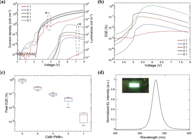
To evaluate the LED performance, current density–voltage– luminance (J–V–L), EQE-voltage characteristics, and external quantum efficiency spectra are recorded and shown in Fig. 4. The J–V characteristics [Fig. 4(a)] of devices show an electrical turn-on at ∼2.2 V, as evidenced by a sharp rise in the current den-sity.13We observe progressive improvement in EQE [Fig. 4(b)] with an increase in CsBr content, consistent with the enhancement in the perovskite film PLQY. The most efficient devices containing a 150 nm thick CsPbBr3emitting layer with a 5:1 precursor ratio have a peak EQE of 1.1% at 5.8 V, which is to our knowledge among the best for perovskite LEDs based on fully evaporated CsPbBr3. The internal quantum efficiency (IQE) of 5.5% can be estimated by divid-ing the peak EQEs with an estimated out-coupldivid-ing factor (∼0.2).40,41 This IQE value suggests a near perfect charge injection and charge
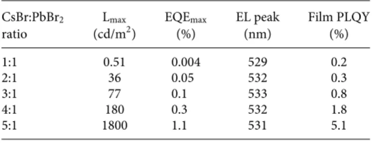
the EQE is dominantly limited by the perovskite film PLQY. As shown inFig. 4(a), the 5:1 device’s luminance rises sharply as the bias is increased beyond 3 V, reaching a maximum luminance of 1800 cdm−2at an applied bias of 6.3 V. The turn-on voltage is 4.4 V (evaluated at a luminance of 1 cd/m2). The device performance of all perovskite LEDs and the corresponding thin film PLQYs is sum-marized in Table I. Statistics of the peak device efficiency is also included inFig. 4(c), which shows excellent device reproducibility within the range of 1:1 to 5:1 CsBr:PbBr2ratios.Figure 4(d)presents the external quantum efficiency spectrum of the perovskite LED under an applied bias of 5.5 V. The spectrum peaks at λ = 531 nm with a FWHM of 21 nm, and no parasitic emission from the adjacent organic layers is observed, indicating efficient carrier recombination solely within the perovskite emitting layer. Under ambient light, a uniform and stable electroluminescence (EL) is visible to the naked eye, as shown in the inset ofFig. 4(d).
In summary, we demonstrate all-vapor-deposited perovskite LEDs based on inorganic CsPbBr3emitters. Fabrication of CsPbBr3 polycrystalline thin films by vapor co-evaporation of precur-sor materials CsBr and PbBr2 enables uniform pinhole-free morphology and precise control over the film thickness and
FIG. 4. Performance of vapor-deposited CsPbBr3perovskite LEDs with different precursor ratios. (a) Current density–voltage–luminance (J–V–L) characteristics. (b)
EQE-voltage characteristics. (c) Statistics of peak EQE of ten devices for each precursor ratio. The red mark in each box represents the median value, and the top and bottom edges of the box indicate the 25th and 75th percentiles, respectively. The error bars represent the maximum and minimum values. (d) Electroluminescence spectrum of the best performing device with a 5:1 precursor ratio. Inset: photo of one of the ten devices on a substrate being operated at an applied bias of 5.5 V.
APL Materials
ARTICLE scitation.org/journal/apmTABLE I. Device performance of all-vapor-deposited CsPbBr3based perovskite LEDs
with different precursor ratios.
CsBr:PbBr2 Lmax EQEmax EL peak Film PLQY
ratio (cd/m2) (%) (nm) (%) 1:1 0.51 0.004 529 0.2 2:1 36 0.05 532 0.3 3:1 77 0.1 533 0.8 4:1 180 0.3 532 1.8 5:1 1800 1.1 531 5.1
stoichiometry. Our best performing device exhibits a peak EQE of 1.1% with the luminance reaching as high as 1800 cd/m2 and EL peak emission at λ = 531 nm with a FWHM of 21 nm. With this and other recent demonstrations of LEDs containing vapor-deposited inorganic cesium halide perovskites,42,43it is clear that evaporative deposition is a viable method for controlling the fabrication of high quality perovskite films, as needed for the LED and possibly future displays and lighting applications.
EXPERIMENTAL METHODS Materials
PbBr2 (99.999%) and CsBr (99.999%) were purchased from Sigma-Aldrich and used without further purifications. LiF (Lumtec, >99.99%), MoO3 (Alfa Aesar, 99.9995%), Tris(4-carbazoyl-9-ylphenyl)amine (TCTA; Lumtec, > 99.5%), 1,3,5-Tris(1-phenyl-1H-benzimidazol-2-yl)benzene (TPBi; Lumtec, >99.5%), and Al (Alfa Aesar, 99.999%) were used as received.
Deposition of perovskite thin film
The perovskite emissive layer (CsPbBr3) is deposited by dual source thermal evaporation from the two precursor materials PbBr2 and CsBr. Two crucible boats loaded with precursor materials are located at the bottom of the evaporator chamber. A quartz crystal monitor is installed above each evaporation source to monitor the film thickness and the rate of evaporation. The tooling factors of two sources are first calibrated individually before the co-evaporation. We set the tooling factor initially to one in the evaporator program. The correct tooling factor is then determined by Tf/Tm, where Tmis the film thickness measured by the quartz crystal monitor and Tfis the actual film thickness measured using ellipsometry. We placed the device samples in a substrate holder above the sources with the film side facing downward. The substrate holder is constantly rotated to make sure uniform deposition throughout the process. As the pres-sure in the chamber reaches 10−6Torr, we start to heat up the source boats and let the materials evaporate for 5–10 min to remove possi-ble volatile impurities. Once the desired deposition rates are reached for both materials, the substrate shutter that separates the source boats and substrate holder is opened to commence deposition. The molar composition of CsBr to PbBr2is varied from 1:1 to 5:1. The molar ratios of the precursors can be calculated from the known film thicknesses, molecular weights, and density of the precursors. We can thus tune the molar ratios simply by changing the deposition
rates of the two precursor materials. The rates are typically fluctuated by less than ±0.2 Å/s and ±0.1 Å/s for CsBr and PbBr2, respectively. The as-deposited film is annealed on a hotplate at 100○
C for 30 min in a nitrogen-filled glovebox before deposition of subsequent layers. Perovskite LED fabrication
Prior to device fabrication, pre-patterned indium-tin-oxide (ITO) substrates (obtained from Thin Film Devices, Inc.) are cleaned by sonication in detergent, de-ionized (DI) water, and acetone (5 min each), followed by boiling in isopropanol twice for 5 min. Oxygen plasma is subsequently used to treat the substrate for 10 min. The substrates are then loaded into a thermal evaporator for subse-quent material depositions. MoO3(5 nm), TCTA (30 nm), CsPbBr3 (150 nm), TPBi (40 nm), LiF (1 nm), and Al (100 nm) are thermally evaporated through a shadow mask at a base pressure of 10−6Torr. The LED active area of 1.21 mm2is determined by the overlap of ITO and Al electrodes. The deposition rates are controlled at 1 Å/s for TCTA and TPBi, 0.5 Å/s for MoO3and LiF, and 3 Å/s for Al. Characterization and testing
Steady-state PL spectra are obtained by exciting the perovskite film with a λ = 405 nm laser and collecting the emission spectra using a Si charge-coupled detector array (Princeton Instruments, Inc. Pixis). A Cary 5000 UV–vis spectrophotometer is used to take the optical absorbance data with a 1 nm wavelength step. The absolute PL quantum yield (PLQY) at room temperature is mea-sured using an integrated sphere in air. Samples are excited with λ = 405 laser light nm at an intensity of 1 mW/cm2. X-ray diffraction (XRD) patterns (2θ scans) are obtained using a Buker D8 diffrac-tometer system with a Cu Kα radiation source. Scanning electron microscopy (SEM) is performed with a Zeiss FESEM Ultra Plus. The film thickness is measured using a Woollam variable-angle spectroscopic ellipsometer.
Perovskite LED device characterization is undertaken inside a nitrogen-filled glovebox. The electroluminescence (EL) spectrum is measured using an Ocean Optics SD2000 fiber-coupled spectrome-ter. Current density–voltage (J-V) characteristics are recorded using a computer-controlled Keithley 2636A source meter. A calibrated Newport 818-UV silicon photodiode is used to measure the optical power output. Luminance and EQE are then calculated by assum-ing the Lambertian emission profile and accountassum-ing for the wave-length dependence (weighted by the device’s EL spectrum) of the photodiode’s responsivity.44
ACKNOWLEDGMENTS
This work was supported, in part, by the National Science Foundation and the U.S. Department of Energy, Center for Exci-tonics (Award No. DE-SC0001088 (MIT)) and made use of the shared facilities supported by the eni-MIT Solar Frontiers Center and managed by the MIT NSF Center for Material Science and Engineering.
REFERENCES 1
H. J. Snaith,J. Phys. Chem. Lett.4, 3623–3630 (2013).
2
M. A. Green, A. Ho-Baillie, and H. J. Snaith,Nat. Photonics8, 506 (2014).
APL Mater. 8, 051113 (2020); doi: 10.1063/1.5144103 8, 051113-5
4
G. Xing, N. Mathews, S. Sun, S. S. Lim, Y. M. Lam, M. Gratzel, S. Mhaisalkar, and T. C. Sum,Science342, 344 (2013).
5S. D. Stranks, S. D. Stranks, G. E. Eperon, G. Grancini, C. Menelaou, M. J. P.
Alcocer, T. Leijtens, L. M. Herz, A. Petrozza, and H. J. Snaith,Science342, 341 (2014).
6C. Wehrenfennig, G. E. Eperon, M. B. Johnston, H. J. Snaith, and L. M. Herz, Adv. Mater.26, 1584 (2014).
7
G. Xing, N. Mathews, S. S. Lim, N. Yantara, X. Liu, D. Sabba, M. Grätzel, S. Mhaisalkar, and T. C. Sum,Nat. Mater.13, 476 (2014).
8M. Saliba, T. Matsui, K. Domanski, J.-Y. Seo, A. Ummadisingu, S. M.
Zakeerud-din, J.-P. Correa-Baena, W. R. Tress, A. Abate, A. Hagfeldt, and M. Grätzel,
Science354, 206 (2016).
9X. Li, Y. Wu, S. Zhang, B. Cai, Y. Gu, J. Song, and H. Zeng,Adv. Funct. Mater. 26, 2435 (2016).
10
Q. A. Akkerman, V. D’Innocenzo, S. Accornero, A. Scarpellini, A. Petrozza, M. Prato, and L. Manna,J. Am. Chem. Soc.137, 10276 (2015).
11J. Song, J. Li, X. Li, L. Xu, Y. Dong, and H. Zeng,Adv. Mater.
27, 7162 (2015).
12L. Protesescu, S. Yakunin, M. I. Bodnarchuk, F. Krieg, R. Caputo, C. H. Hendon,
R. X. Yang, A. Walsh, and M. V. Kovalenko,Nano Lett.15, 3692 (2015).
13
Z.-K. Tan, R. S. Moghaddam, M. L. Lai, P. Docampo, R. Higler, F. Deschler, M. Price, A. Sadhanala, L. M. Pazos, D. Credgington, F. Hanusch, T. Bein, H. J. Snaith, and R. H. Friend,Nat. Nanotechnol.9, 687 (2014).
14
K. Lin, J. Xing, L. N. Quan, F. P. G. de Arquer, X. Gong, J. Lu, L. Xie, W. Zhao, D. Zhang, C. Yan, W. Li, X. Liu, Y. Lu, J. Kirman, E. H. Sargent, Q. Xiong, and Z. Wei,Nature562, 245 (2018).
15
T. Chiba, Y. Hayashi, H. Ebe, K. Hoshi, J. Sato, S. Sato, Y.-J. Pu, S. Ohisa, and J. Kido,Nat. Photonics12, 681 (2018).
16Y. Zou, Z. Yuan, S. Bai, F. Gao, and B. Sun,Mater. Today Nano
5, 100028 (2019).
17M. Kulbak, D. Cahen, and G. Hodes,J. Phys. Chem. Lett.
6, 2452 (2015).
18Y. Rakita, N. Kedem, S. Gupta, A. Sadhanala, V. Kalchenko, M. L. Böhm,
M. Kulbak, R. H. Friend, D. Cahen, and G. Hodes,Cryst. Growth Des.16, 5717 (2016).
19L.-P. Cheng, J.-S. Huang, Y. Shen, G.-P. Li, X.-K. Liu, W. Li, H. Wang,
Y.-Q. Li, Y. Jiang, F. Gao, C.-S. Lee, and J.-X. Tang,Adv. Opt. Mater.7, 1801534 (2019).
20L. Song, X. Guo, Y. Hu, Y. Lv, J. Lin, Z. Liu, Y. Fan, and X. Liu,J. Phys. Chem. Lett.8, 4148 (2017).
21
Y. Ling, Y. Tian, X. Wang, J. C. Wang, J. M. Knox, F. Perez-Orive, Y. Du, L. Tan, K. Hanson, B. Ma, and H. Gao,Adv. Mater.28, 8983 (2016).
22N. Yantara, S. Bhaumik, F. Yan, D. Sabba, H. A. Dewi, N. Mathews, P. P. Boix,
H. V. Demir, and S. Mhaisalkar,J. Phys. Chem. Lett.6, 4360 (2015).
23
S. Reineke, F. Lindner, G. Schwartz, N. Seidler, K. Walzer, B. Lüssem, and K. Leo,Nature459, 234 (2009).
24L. K. Ono, S. Wang, Y. Kato, S. R. Raga, and Y. Qi,Energy Environ. Sci. 7, 3989 (2014).
C.-Z. Ren-Wu, C.-Y. Chen, and H.-W. Lin,Adv. Mater.28, 7013 (2016).
26C.-W. Chen, W. Kang, S.-Y. Hsiao, P.-F. Yang, K.-M. Chiang, and
H.-W. Lin,Adv. Mater.26, 6647 (2014).
27
M. Liu, M. B. Johnston, and H. J. Snaith,Nature501, 395 (2013).
28
C.-Y. Chen, H.-Y. Lin, K.-M. Chiang, W.-L. Tsai, Y.-C. Huang, C.-S. Tsao, and H.-W. Lin,Adv. Mater.29, 1605290 (2017).
29Q. Ma, S. Huang, X. Wen, M. A. Green, and A. W. Y. Ho-Baillie,Adv. Energy Mater.6, 1502202 (2016).
30
C. C. Stoumpos, C. D. Malliakas, J. A. Peters, Z. Liu, M. Sebastian, J. Im, T. C. Chasapis, A. C. Wibowo, D. Y. Chung, A. J. Freeman, B. W. Wessels, and M. G. Kanatzidis,Cryst. Growth Des.13, 2722 (2013).
31
M. Nikl, E. Mihokova, K. Nitsch, F. Somma, C. Giampaolo, G. P. Pazzi, P. Fabeni, and S. Zazubovich,Chem. Phys. Lett.306, 280 (1999).
32Y. Ling, L. Tan, X. Wang, Y. Zhou, Y. Xin, B. Ma, K. Hanson, and H. Gao, J. Phys. Chem. Lett.8, 3266 (2017).
33
M. Ban, Y. Zou, J. P. H. Rivett, Y. Yang, T. H. Thomas, Y. Tan, T. Song, X. Gao, D. Credgington, F. Deschler, H. Sirringhaus, and B. Sun,Nat. Commun.9, 3892 (2018).
34
L. N. Quan, R. Quintero-Bermudez, O. Voznyy, G. Walters, A. Jain, J. Z. Fan, X. Zheng, Z. Yang, and E. H. Sargent,Adv. Mater.29, 1605945 (2017).
35H. Cho, S.-H. Jeong, M.-H. Park, Y.-H. Kim, C. Wolf, C.-L. Lee, J. H. Heo,
A. Sadhanala, N. Myoung, S. Yoo, S. H. Im, R. H. Friend, and T.-W. Lee,Science 350, 1222 (2015).
36L. Zhao, Y.-W. Yeh, N. L. Tran, F. Wu, Z. Xiao, R. A. Kerner, Y. L. Lin, G. D.
Scholes, N. Yao, and B. P. Rand,ACS Nano11, 3957 (2017).
37
X. Lian, X. Wang, Y. Ling, E. Lochner, L. Tan, Y. Zhou, B. Ma, K. Hanson, and H. Gao,Adv. Funct. Mater.29, 1807345 (2019).
38
Z. Li, B. Jiao, Z. Wu, P. Liu, L. Ma, X. Lei, D. Wang, G. Zhou, H. Hu, and X. Hou,
J. Mater. Chem. C1, 2183 (2013).
39
Q. Shan, J. Li, J. Song, Y. Zou, L. Xu, J. Xue, Y. Dong, C. Huo, J. Chen, B. Han, and H. Zeng,J. Mater. Chem. C5, 4565 (2017).
40
Q. Zhang, M. M. Tavakoli, L. Gu, D. Zhang, L. Tang, Y. Gao, J. Guo, Y. Lin, S.-F. Leung, S. Poddar, Y. Fu, and Z. Fan,Nat. Commun. 10, 727 (2019).
41N. Wang, L. Cheng, R. Ge, S. Zhang, Y. Miao, W. Zou, C. Yi, Y. Sun, Y. Cao,
R. Yang, Y. Wei, Q. Guo, Y. Ke, M. Yu, Y. Jin, Y. Liu, Q. Ding, D. Di, L. Yang, G. Xing, H. Tian, C. Jin, F. Gao, R. H. Friend, J. Wang, and W. Huang,Nat. Photonics10, 699 (2016).
42
J. Li, P. Du, S. Li, J. Liu, M. Zhu, Z. Tan, M. Hu, J. Luo, D. Guo, L. Ma, Z. Nie, Y. Ma, L. Gao, G. Niu, and J. Tang,Adv. Funct. Mater29, 1903607 (2019).
43P. Du, J. Li, L. Wang, J. Liu, S. Li, N. Liu, Y. Li, M. Zhang, L. Gao, Y. Ma, and
J. Tang,ACS Appl. Mater. Interfaces11, 47083 (2019).
44S. R. Forrest, D. D. C. Bradley, and M. E. Thompson,Adv. Mater. 15, 1043 (2003).