Characterization of Optical Interconnec
by
AShiou Lin Sam
B.S., Electrical Engineering
University of Maryland at College Park, 1998
Submitted to the Department of Electrical Engineeri
and Computer Science
in partial fulfillment of the requirements for the degree of
ENG
SSACHUSETTS INSTITUTEOF TECHNOLOGY
JUN 2 2 2000
Master of Science in Electrical Engineering and Computer Science
at the
MASSACHUSETTS INSTITUTE OF TECHNOLOGY
@
Massachusetts Institute
oay 2000
o Technology 2000. All rights reserved.
A u th or ... .. . . ...-
-Department f Electrical Engineering
and Computer Science
May 18, 2000
Certified by...--
-Duane Boning
Associate Professor of Electrical Engineering
and Computer Science
Thesis Supervisor
Certified by...
....
Accepted by...
Anantha Chandrakasan
Associate Professor of Electrical Engineering
and Computer Science
'Visor
Arthur C. Smith
Chairman, Departmental Committee on Graduate Students
Characterization of Optical Interconnects by
Shiou Lin Sam
Submitted to the Department of Electrical Engineering and Computer Science
on May 18, 2000 in partial fulfillment of the requirements for the degree of
Master of Science in Electrical Engineering and Computer Science Abstract
Interconnect has become a major issue in deep sub-micron technology. Even with copper and low-k dielectrics, parasitic effects of interconnects will eventually impede advances in integrated electronics. One technique that has the potential to provide a paradigm shift is optics. This project evaluates the feasibility of optical intercon-nects for distributing data and clock signals. In adopting this scheme, variation is introduced by the detector, the waveguides, and the optoelectronic circuit, which includes device, power supply and temperature variations. We attempt to charac-terize the effects of the aforementioned sources of variation by designing a baseline optoelectronic circuitry and fabricating a test chip which consists of the circuitry and detectors. Simulations are also performed to supplement the effort. The results are compared with the performance of traditional metal interconnects. The feasibility of optical interconnects is found to be sensitive to the optoelectronic circuitry used. Variation effects from the devices and operating conditions have profound impact on the performance of optical interconnects since they introduce substantial skew and delay in the otherwise ideal system.
Thesis Supervisor: Duane Boning
Title: Associate Professor of Electrical Engineering and Computer Sciences
Thesis Supervisor: Anantha Chandrakasan
Acknowledgments
I would like to thank Professor Boning and Professor Chandrakasan for their time and effort in guiding and motivating this work. Their encouragement and trust were crucial to the completion of the project.
I would also like to thank Kush for his willingness and selflessness in providing insights
and enlightening suggestions whenever I encountered problems along the way. I am grateful to Desmond and Andy for imparting their knowledge of device physics and for assisting in the design and testing of the detector. In addition, I want to thank Paul-Peter for his assistance in building the prototype. Heartfelt appreciation is extended to Jim and Illiana for offering invaluable help during the layout of the chip.
I want to thank Rong-Wei for his constant support, be it emotional or technical, and
for his belief in my ability, more so than myself.
Lastly, I would like to thank my family for their love, support, and sacrifices. father, for offering insights and inspirations; my mother, for the loving care gentle encouragements; my little brother, for the mysteriously timed phone calls laughter that we share.
My
and and
This research was supported in part by the Interconnect Focus Center under MARCO and DDRE funding and by an NSF Graduate Fellowship.
Contents
1 Introduction 1.1 Background . . . . 1.2 O utline. . . . . 2 Optoelectronic Circuitry 2.1 Transimpedance Amplifier . . . . 2.2 Postamplifier . . . . 2.3 Feedback Circuitry . . . . 2.4 Complete Receiver . . . . 3 Variation Effects 3.1 Statistical Modeling . . . .3.1.1 Process Oriented Approach
3.1.2 Device Oriented Approach
3.1.3 Inter-Die Variations Approach 3.1.4 Intra-Die Variations Approach
3.2 W aveguide . . . . 3.3 Detector .. .. ... . . . . 12 12 14 15 20 22 25 27 29 . . . . 30 . . . . 30 . . . . 31 . . . . 32 . . . . 32 . . . . 35 .. . . . .. 35
3.4 Receiver Circuitry . . . . 3.4.1 Process Variation . . . . 3.4.2 Power Supply Variation . . . . 3.4.3 Operating Temperature Variation . . . . .
3.5 Summary of Process and Environmental Variation
4 Optical and Cu Interconnect
4.1 Variation Effects on Copper Interconnect 4.1.1 Interconnect Delay . . . . 4.1.2 Clock Skew . . . . 4.2 Comparison Between Optical and Copper 4.2.1 Power Requirement . . . . 4.2.2 Clock Distribution . . . . 4.2.3 Signal Propagation . . . .
Interconnect
5 Implementation and Testing
5.1 Physical Realization . . . . 5.2 Test Chip Results . . . .
5.2.1 Possible Solutions . . . .
5.2.2 Testing of Receiver Module . . . .
6 Test Chip Revision
6.1 Detector . . . .. . . . . 6.2 Receiver Module . . . . Effects . . 38 . . 39 44 . . 44 . . 46 47 47 48 50 52 53 54 55 56 57 58 60 61 63 63 65
6.2.1 Power Supply Sensitivity . . . .
6.2.2 Receiver Circuit Topology . . . .
7 Conclusion and Future Work 7.1 Conclusion ... 7.1.1 Optoelectronic Circuitry 7.1.2 Detectors . . . . 7.2 Future Work . . . . 7.2.1 Optoelectronic Circuitry 7.2.2 Optoelectronic Devices 7.2.3 Integration . . . . 7.2.4 Variation Analysis . . . Bibliography 65 65 69 . . . . 6 9 . . . . 6 9 . . . . 70 . . . . 70 . . . . 7 1 . . . . 7 1 . . . . 7 1 . . . . 7 1 72
List of Figures
1-1 Delay for Local and Global Wiring versus Feature Size [26]. .
2-1 One-driver Grid, Two-driver Grid and Windowpane grid . . 2-2 H-tree Clock Distribution. . . . .
2-3 Global Optical Clock Distribution. . . . .
2-4 Receiver Circuitry Block Diagram. . . . .
2-5 Optoelectronic Circuitry Block Diagram. . . . . 2-6 Generalized Transimpedance Amplifier. . . . . 2-7 Small Signal Model of Transimpedance Amplifier. . . . . 2-8 Preamplifer, based on [13]. . . . .
2-9 Voltage Am plifier. . . . . 2-10 Small Signal Model of Voltage Amplifier. . . . . 2-11 Simplified Small Signal Model of Voltage Amplifier. . . . . . 2-12 Replica Biasing. . . . .
2-13 Shifter Circuit. . . . .
2-14 Comparator Integrated with LP Filter. . . . .
2-15 Complete Receiver Circuitry. . . . . 2-16 Simulation Results at 1GHz. . . . . 13 . . . . 15 . . . . 16 . . . . 17 . . . . 18 . . . . 19 . . . . 20 . . . . 20 . . . . 22 . . . . 23 . . . . 23 . . . . 23 . . . . 25 . . . . 26 . . . . 26 . . . . 27 . . . . 28
3-1 3-2 3-3 3-4 3-5 3-6 3-7 3-8 3-9
Process Oriented IC simulation. . . . . Simulation Scheme for Process Level Variation. Device Oriented Approach. . . . .
Simulation Flowchart. . . . .
Flow Chart for Variations Effect Simulation. . . Methodology for Simulating Variation Effects in Polysilicon Waveguide. . . . . Receiver Circuitry for 100pA Input Current. Receiver Circuitry for 1mA Input Current. .
3-10 Standard Deviation of VT mismatch, oA,, versus Area for a .35pum
process.
3-11 VT for NMOS Device versus the Standard Deviation for a .35pm Process 3-12 VT for PMOS Device versus Standard Deviation for a .35pm Process. 3-13 Effects of VT Variation on Clock Skew for Optical Clock Receiver. . .
3-14 Cross Section Diagram of a MOS Device. . . . .
3-15 Effects of LP01Y on Clock Skew for Optical Clock Receiver. . . . . 3-16 Effects of Power Supply Variation on Clock Skew for Optical Clock
R eceiver. . . . .
3-17 Effects of Temperature Variations on Skew for Optical Clock Receiver.
4-1 4-2 4-3 4-4
Effects of Copper Damascene CMP. . . . . Methodology for Assessing the Impact of Spatial Variation. .
Profilometry Trace of Array of Interconnects after CMP. . .
Interconnect Distributed RC Delay . . . .
. . . . 30 . . . . 31 . . . . 32 . . . . 33 . . . . 34 Detector. . . . . 35 . . . . 35 . . . . 37 . . . . 37 . . . . 4 0 41 42 42 43 44 45 45 48 49 50 50
Effects of Cu CMP on Bus Delay The Clock Distribution Circuit [9]. Percentage of Poly Length Variation 4-5 4-6 4-7 5-1 5-2 5-3 5-4 5-5 5-6
5-7 Test Chip Output Shown in the Upper Trace.
6-1 Cross Sectional View of Detector. . . . .
6-2 Cross Sectional View of Twin Tub Detector.
6-3 Conventional Preamplifier Configurations.
6-4 Modified Preamplifier Configurations...
6-5 Automatic Gain Control Circuit. . . . . 6-6 Offset Circuit. . . . .
Silicon p-i-n Diode. . . . . Die Picture. . . . . Top View of Detector. . . . . . Cross Section of Detector. . . .
Test Chip. . . . . Test Chip Output Shown in the
51 52 52 . . . . 5 7 . . . . 5 8 . . . . 5 9 . . . . 5 9 61 62 62 64 65 66 66 67 67 Lower Trace.
List of Tables
3-1 3-2 3-3 4-1 4-2 4-3Impact of Input Current on Skew . . . .
Impact of Input Current on Delay . . . .
Sensitivity of Variation Parameters. . . . .
Interconnect Parameters. . . . .
Variation Impact on Conventional Clock Skew
Variation Impact on Optical Clock Skew . . .
5-1 Thickness of Various Layers Used in the Process
. . . . . 37 . . . . . 38 . . . . . 46 52 53 55 . . . . 60
Chapter 1
Introduction
1.1
Background
As technology continues to scale into deep sub-micron regions, there is a correspond-ing increase in chip size and device speed. Whereas transistor scalcorrespond-ing provides si-multaneous improvements in both density and performance, interconnect scaling im-proves interconnect density but generally at the cost of degraded interconnect delay, as illustrated in Figure 1-1. Results of theoretical modeling indicate that below 1pm minimum feature size, interconnect delay due to parasitic capacitance, including both fringe and inter-wire coupling capacitance, will have a strong impact on circuit perfor-mance [2]. As a result, effects of interconnects, which previously have been regarded as trivial, are becoming more prominent. These effects include bus delays, clock skews, coupling signal noise, and power and ground noise. To address these problems, active research has resulted in the following technological trends [14].
* Increasing the aspect ratio
"
Reducing dielectric constant" Reducing resistivity of metal lines
1 n Z) 0r 10 0.1 250 180 130 100 180 130 100
Process Technology Node (nm)
70 50 35
Figure 1-1: Delay for Local and Global Wiring versus Feature Size [26].
Yet, studies have shown that even with copper and low-k dielectrics, these approaches will eventually encounter limits and may impede advances in integrated electronics
[18]. New, revolutionary techniques are needed to provide a paradigm shift to continue
the progress in integrated electronics. One technique that has the potential to solve many of the underlying physical problems while continuing to scale is optics. However, there are many practical challenges awaiting to be addressed. The technology is still in its infantile stage and the systems that could benefit most from optics are likely to be different from the architectures of today, which are optimized around the strengths and weaknesses of electrical interconnects [18]. Moreover, there are many technical challenges in implementing dense optical interconnects in silicon CMOS chips. These include circuit issues, integration techniques, and development of appropriate optical technology to allow low-cost optical modules.
-$--Gate Delay (Fan out 4) " Local (Scaled) at" ( p_
(Scaled Die Edge)
-X Gl da w/oRepeaters
In this work, we attempt to evaluate the feasibility of optical interconnects from the following perspectives:
" Circuit Issues
" Clock Distribution and Data Routing Applications " Susceptibility to Variation Effects
" Superiority Compared to Copper Interconnects
1.2
Outline
One of the largest challenges for future interconnects is high-speed global clock distri-bution. Much of this thesis is focused on evaluation of the feasibility for use of optical interconnect to meet this challenge. In Chapter 2, we describe the component archi-tecture for global optical clock distribution with local electrical distribution. The op-toelectronic circuitry required to interface to the global clock is also presented. Next, in Chapter 3, the effects of variation from various components in the optical clocking scheme are discussed, along with the presentation of simulation results. The sensitiv-ity of the combined optical-electronic clock to these variations is a key concern; these variations and sensitivities will introduce skew and limit the clock speed achievable. Chapter 4 illustrates the comparison between optical and conventional metal inter-connects, including global data communication as well as clock distribution. Chapter
5 presents the physical realization of the baseline optoelectronic receiver circuit and
measurement results. Chapter 6 details suggestions and revision ideas for the receiver circuit. Chapter 7 concludes with possible future work and research directions.
Chapter 2
Optoelectronic Circuitry
Conventional clock distribution falls into two categories, equipotential clocking and H-tree clocking. Equipotential clocking entails distributing a global clock signal to the chip as a regular signal line, as illustrated in Figure 2-1. Since equipotential clocking assumes that the resistance in the wires is negligible and that the entire net is a uniform voltage, this clocking method causes skew when the RC time constant of the nets become significant due to the scaling of feature sizes. In order to achieve the same performance as clock speed increases, the 300MHz and 600MHz Alpha chips used two drivers and subsequently four top level buffers [1]. This is done because only smaller sections of the chip can be modeled as equipotentials at higher frequencies.
Driver Driver Driver
Grid Grid - -Grid
H-trees, on the other hand, are based on the symmetry of the clock net, as shown in Figure 2-2. The clock distribution system is laid out in a way such that the distance between the center of the net to each of the tips is always the same. This would result in the signals arriving at the tips at the same time. H-trees, however, are affected by intra-die variations. Line-width variations and temperature gradients, for example, will result in skew.
tip
center
Figure 2-2: H-tree Clock Distribution.
A more novel approach consists of using an array of synchronized Phase-Lock Loops
(PLL) [12]. Independent oscillators generate the clock signal at multiple points across a chip; each oscillator distributes the clock to only a small section of the chip. Phase detectors (PD) at the boundaries between the tiles produce error signals that are summed in each tile and are used to adjust the frequency of the node oscillator. This approach is currently still being researched and tested.
Photon Source optoelectronic circuitry waveguides electrical clock distribution
Figure 2-3: Global Optical Clock Distribution.
In this work, we consider optical clocks. Optical clocks can be transmitted in a tree using waveguides or in freespace. The limitation of optical interconnects, in both cases, is their inability to operate as a stand alone module. In order to utilize optics for on-chip communications, optoelectronic circuitry is required to serve as an interface. In this thesis, we focus on developing a baseline optoelectronic circuit for use with waveguide transmission. Figure 2-3 illustrates the component architecture for global optical clock signal distribution with local electrical distribution. The chip is divided into smaller sections, and each section consists of a detector and a receiver module. The global clock is distributed from the photon source (the most popular choice being a laser for its ease of use) through waveguides with splitters and bends to each of the sections. Once reaching the detector in each section, the global clock optical pulses are converted into current pulses. These current pulses feed into the transimpedance amplifier of the optoelectronic circuitry and are amplified into voltage signals, which are distributed through conventional metal interconnects as electrical clock signals. The motivation behind such a hybrid clock distribution system is that smaller areas on chip are exposed to less intra-die variation due to locality. Thus, as long as a skew-free signal is distributed to the nodes, conventional H-tree distribution can be used within the smaller region. Figure 2-3 illustrates 16 smaller sections, but the optimal number of sections depends on the chip size and variation effects. A similar scheme can also be employed for routing data on chip. In the case of clock
distribution, clock skew is the parameter of concern; however, for data distribution the absolute delay is much more important than skew.
Receiver designs generally break down into the block diagram in Figure 2-4. Incom-ing current pulses from the detector are amplified into voltage pulses through the preamplification stage, depicted as a transimpedance amplifier in the figure. Due to amplification and bandwidth requirements, voltage amplifiers usually follow as the next stage in the design. Some designs incorporate a decision circuit as the final stage for converting the signal into a rail-to-rail digital circuit. Others use buffers to achieve the same purpose. The designs for each module can be implemented as either a single-ended or a double-ended topology.
Detector Transimpedance Voltage Decision
Amplifier Amplifier Circuit Figure 2-4: Receiver Circuitry Block Diagram.
Woodward et al. [27] has implemented a single-ended receiver design that operates up to 500MHz. The design consists of an inverter-based transimpedance amplifier, followed by a second stage voltage amplifier implemented as an inverter with a diode-connected device, and a buffer before the output. The output of the preamplifier is fed into digital logic elements designed to generate zero skew differential output signals. These signals are applied to off-chip driver circuits.
Ingels et al. [8] designed a single-ended receiver circuitry using a feedback resistor around a string of modified inverters. It uses a replica biasing circuit in order to accurately bias the inverters. The system achieves a gain of 18THzQ, which makes it capable of amplifying current in the MA region at the expense of a lower bandwidth of 120MHz.
Tanabe et al. [5] approached the design using a differential-ended circuit. The design consists of a preamplifier, an automatic gain control, a PLL and demultiplexers. The design was implemented in a 0.15ptm process and achieves a bandwidth of 1.2GHz. In this work, we develop a baseline optoelectronic circuit [13] to investigate the fea-sibility of optical interconnects. In order to integrate dense optical interconnects on-chip, the optoelectronic circuitry power dissipation is kept in the mW range. The circuitry operates at a bandwidth of 1GHz on a single power supply voltage in order to facilitate integration with a standard CMOS process without the use of analog extensions. Figure 2-5 provides a block diagram illustration of the optoelectronic circuitry consisting of a preamplification and a postamplification stage. The pream-plifier is required in order to convert the current generated by the photodetector upon receiving optical excitation into a voltage signal. It amplifies a 1OpA current from the photodetector into a voltage signal with a 10mV amplitude. This voltage signal is further amplified through the postamplification stage into a rail-to-rail voltage swing of 3.3V, which serves as the on-chip clock. The circuit details are presented in the following sections. The photodiode is modeled as a current source in parallel with a diode capacitance and diode resistance.
Vout
Preamplifier Voltage Amplfier
Vbias
Feedback Circuitry
2.1
Transimpedance Amplifier
Rf
CdiodeTCin Cout Cload
Figure 2-6: Generalized Transimpedance Amplifier.
A Rf B
lin
CTVin
RL
_
VFigure 2-7: Small Signal Model of Transimpedance Amplifier.
A generalized transimpedance amplifier and its small signal model are shown in Figure 2-6 and 2-7. RL includes the output resistance of the transimpedance amplifier and
the load resistance. Cout is the output capacitance of the amplifier and Coad is the load capacitance. Cdiode represents the diode of the capacitance and C, denotes the input capacitance of the transimpedance amplifier. Rf is the feedback resistor used in the preamplifier. The CT shown in the small signal model is the summation of
Cdiode and Cj, where Co includes COt and
CLoad-Summing currents at node A in the small signal model, we obtain the following
Iin = VinsCT + (1) Rf At node B, GmVin+ VosCo+ " = 0 (2) RL Rf Simplifying Equation 2,
-v
- + sCO + I Vin = -VO( Rf G 1 L) (3) m RfSubstituting Equation 3 into Equation 1,
In = -Vo( ' L )(sC + VO (4)
G'i- T Rf
Rf
Vo LgRLRf( - Gm)
VO
Rf+ S2(5)Iin 1 + GmRL + s(CORL + CTRL + CTRI) + s2(CoCTRf RL)
Thus, the transfer function at DC value, Zf, and pole, pi, are
RLRf ( - Gm)
Zf = !(6 )
1 + GmRL
Pi = (7)
CT(RL + RJ) +CoRL
The following assumption
CT > CO (8)
results in W3, given by the following:
Wd = +GmRL (9)
dB CT(RL + Rf)
Looking at Equation 6, we notice that with a high Gm, the absolute gain of the transimpedance amplifier can be estimated as the value of the feedback resistor, Rf.
W3dB, as shown in Equation 9, is a function of the gain, 1 + GmRL and the RC time constant of the circuit.
The CMOS implementation of the 1GHz transimpedance amplifier [13] is presented in Figure 2-8. It is based on a gm/gm amplifier with a feedback resistor implemented as a PMOS transistor operating in linear region (M4 in the figure), with the resistance given by
R. 1 (10)
The well, being connected to the drain, results in only a small degradation in band-width as the well capacitance is added to the input node. The transimpedance am-plifier takes a current input of 1OpA and converts it into a voltage signal with an amplitude of lOmV. MI and M3 form an inverter configuration. M2 is added in order to increase the bandwidth of the preamplifier.
Using the approximation that the gain can be estimated as the value of the feedback resistor, we designed for Rf to be around lkQ. CT was estimated to be 100fF (the diode capacitance) and RL was estimated to be the load resistance of the next stage, which is a level shifter. These parameters were used as a starting point in the design of the 1GHz transimpedance amplifier and further iterated with simulations.
Vdd M4
L_
M3-SM M2
Figure 2-8: Preamplifer, based on [13].
2.2
Postamplifier
The signal has to be further amplified through postamplifiers into the desired rail-to-rail signal due to the insufficient gain from the preamplifier. This can be accomplished through a string of inverters biased at their threshold voltages. The first inverters act as linear amplifiers due to the small input signal. Closer to the final stages, clipping occurs at the rails. Thus, a larger input will merely result in a shift forward of the
first clipping. As a result, we have avoided automatic gain control at the expense of accurately biasing of the inverters. This is accomplished through replica biasing
[13],
as shown in Figure 2-12.
Conventional inverters are unable to achieve a high bandwidth due to their inherent gain. Thus, modified inverters are used. Figure 2-9 illustrates such an inverter. The diode connected NMOS shifts the second-order pole to higher frequencies by reducing the small-signal impedance on the inverter's output node. The gain is also limited as a result. The small signal circuit is shown in Figure 2-10; using the source-absorption theorem, a simplified small signal model is obtained, shown in Figure 2-11.
Vdd
M3
M2
In _Out
M1
Figure 2-9: Voltage Amplifier.
Vin _ 9m1V+
1 gm
3Vs 2Vro
Figure 2-10: Small Signal Model of Voltage Amplifier.
+-. r 0 0
Vin + gm1V gm3V r 19m r02
Figure 2-11: Simplified Small Signal Model of Voltage Amplifier. From the model, we can derive the gain of the amplifier:
Vn = V S(11)
Vout _m1 + gm 3 (13) Vin 9ds1 + gs2 + 9ds3 + 9m2 Assuming 9m2>9s2 + gds1 + gds3 Equation 13 simplifies to Vot _ gmi + gm3 (14) in 9m2
Where without M2, the gain would be
Vout _ Ymi + gm3 (15)
Vin 9ds1 + 9s2 + 9ds3
The W3dB is given by the following:
1
W3dB = (16)
RoutCout
where, in the case where M2 is included, Rout is approximately
Rout = (17)
9m2
and Cout is given by
Cout = Cload + Cdl + Cdb1 + Cgs3 + Csb3 + Cgs2 + Csb2 (18)
Thus, W3dB is increased by the transconductance of M2 while the gain is reduced simultaneously. In this design, three of these modified inverters are cascaded together in order to obtain sufficient gain for a single stage. A single stage was designed to have a gain of 20dB with a cutoff frequency of 1GHz.
2.3
Feedback Circuitry
One critical issue in using the above circuitry is accurate biasing. Inaccurate biasing of the inverter strings will lead to a degraded duty cycle. In this work, replica biasing, as shown in Figure 2-12, is used.
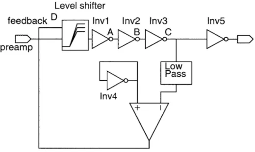
Level shifter feedback 1 nv2 lnv3 lnv5 pream C > -Low L> _ Pass Inv4 +
Figure 2-12: Replica Biasing.
The feedback circuitry consists of a level shifter (Figure 2-13), a comparator (Figure 2-14) and a low pass filter. The low pass filter obtains the DC value of the string of inverters at node C. This DC value is compared (through the comparator) to the threshold voltage of Inverter 4, which is a replicate of the string of inverters. The output of the comparator will adjust the level shifter accordingly. The output of the level shifter increases with decreasing input value and vice versa. For example, when node C a has DC value greater than the threshold of the inverter, the comparator will have a voltage smaller than the nominal value. This will cause the DC voltage at the output of the level shifter to increase. As a result, the DC voltage at node
A will decrease while the value at node B will increase and the value at node C will
decrease. This negative feedback will result in the convergence of the DC biasing for the inverters.
Vdd
feedback
M3
M2
Out
preamp
JO
SM1
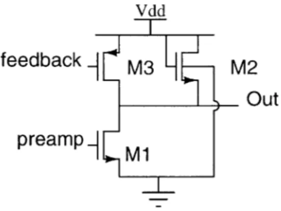
Figure 2-13: Shifter Circuit.
Since the shifter is in the signal path, it is designed with a bandwidth comparable to the modified inverters, with only a small gain, given by the following equation. It results from an analysis similar to that of Equation 14, but with 9m3 removed as M3 is feedback connected:
A 9 (19)
9m2
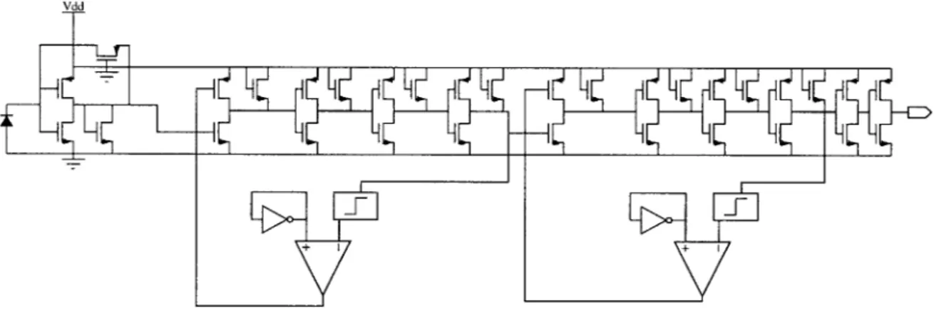
The comparator, as shown in Figure 2-14 has a DC gain of 120, with a bandwidth of around 45KHz. To obtain the low pole, a capacitor is placed in Miller configuration. The zero introduced by the Miller capacitor is nulled by a resistor, a technique widely used in operational amplifier designs. In order to ensure stability of the feedback circuitry, a low corner frequency is used.
Vdd M M4 M5 preamp bia%1 M1 M2 inverter.output M7 M6
2.4
Complete Receiver
The complete receiver
[13]
is shown in Figure 2-15. The input current is converted into a voltage signal through the preamplifier, it is further amplified by 20dB through the second stage, which consists of a level shifter, three modified inverters and a feedback system for DC biasing. Since a single post amplification stage is insufficient for the input current that we are considering, a second post amplification stage, identical to the first, is added. The final output is buffered into a rail-to-rail voltage swing. The transient simulation results are shown in Figure 2-16.Vdd
+ I + I
Figure 2-15: Complete Receiver Circuitry.
Currents (tin) !Q fA PI 9 c c l
b.~
!E bo, Cft ft f ftIIIq
--INZ( W 00 0%~
IND
-4 -- ---000 N 44--
----S _- -0 Voltages (tin)Chapter 3
Variation Effects
As devices continue to scale down, variation effects are becoming more prominent and are causing substantial performance degradation in designs. In large chips, spatial pattern dependent interconnect and device variations result in clock skew and delay
[16]. In analog designs, much effort has been concentrated on device matching since
mismatch will sometimes reduce design yield.
In conventional interconnects, spatial dependent interconnect variation and device variation results in clock skew and data bus delay. In implementing the clocking scheme suggested in Chapter 1, variation stems from three sources: the waveguide, the detector and the receiver circuitry. We will study the individual contributions of these aforementioned sources to the total clock skew.
In this chapter, we first review several approaches currently being used to understand effects of variation, and then present our methodology and results for analyzing vari-ation effects on the optical module and the circuitry.
3.1
Statistical Modeling
Several approaches have been used to model process variations. In the following sections, we present a brief overview of some of the approaches.
3.1.1
Process Oriented Approach
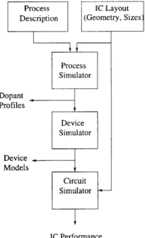
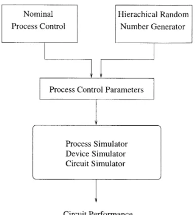
A process oriented approach to variation analysis uses a process simulator, a device
simulator, and a circuit simulator, as shown in Figure 3-1. The process simulator takes in the process description along with an IC layout and generates physical and geometry characteristics such as dopant profiles and thicknesses of various layers. These outputs are fed into a device simulator which produces device results suitable for device parameter extraction; these device models then form the inputs to the circuit simulator. Variations can be introduced into the process description in order to understand the effects, resulting in the scheme shown in Figure 3-2
[19].
Process IC Layout
Description (Geometry, Sizes]
Process Simulator Dopant Profiles Device Simulator Device Models Circuit Simulator IC Performance
Nominal Hierachical Random Process Control Number Generator
Process Control Parameters
Process Simulator Device Simulator
Circuit Simulator
Circuit Performance
Figure 3-2: Simulation Scheme for Process Level Variation.
3.1.2
Device Oriented Approach
A device-oriented approach to variation analysis, on the other hand, is based on device model parameter extraction from measured I-V curves, as shown in Figure 3-3. Measurements for different sets of transistors taken from different areas on the chip are conducted and plotted. The model parameters extracted from the I-V curves
will exhibit statistical variations and correlations. In using this approach, it is often
assumed that independent variation occurs between the model parameters and that
the circuit would be operational over an arbitrary combination of the variations of parameters such as threshold voltage, body effect and oxide thickness. This will lead to inaccurate characterization of the IC process variations. For example, independent
variation between Vn and Vt, would overestimate the variability of a transistor since
the correlation of V1
Process Device I-V Curve Parameter Model
Disturbances Variation Parameter
Measuremen Extraction Variation
Figure 3-3: Device Oriented Approach.
3.1.3
Inter-Die Variations Approach
Statistical analysis using inter-die variation usually assumes that process disturbances affect devices within the same chip in the same way, i.e., intra-die variations are negli-gible. In using this approach, one would need to choose a set of model parameters (for forming a parameterized inter-die statistical model) to characterize the device varia-tions. This lends utmost importance to identifying the critical model parameters. All other parameters can then be generated from this set using regression dependencies.
The parameters are generally chosen using factor analysis and principle component analysis [4], which account for the correlations between the different device parameters (e.g., between V, and VtT). A regression model is then built from these parameters.
3.1.4
Intra-Die Variations Approach
The above approximation approach would be acceptable for digital circuits, but in cases where device matching is important, it would lead to significant error. The most common example is matching in analog circuit blocks, where mismatch would cause an offset in the output. The research on intra-die variation has mostly focused on the mismatch variance [17], [11], [22]. One approach taken by [17], as shown in Figure 3-4, is most interesting because it is capable of generating statistically significant models from intra- and inter-die parameters. It uses statistical parameter analysis to obtain parameter means, correlations and standard deviations as a function of device size and spacing. Principal component analysis and --space analysis are performed on these parameters. In using PCA, correlations within transistor are preserved while
o-space analysis preserves variance between transistors. The output from PCA and o--space form the input for generation of model decks. The model decks and circuit description are then used for circuit simulation.
Statistical Parameter Analysis
Principal Component T - Space Circuit
Analysis Analysis Description
Random Number Generator Model Integration Circuit Simulation
Figure 3-4: Simulation Flowchart.
The initial phase of our work closely resembles the inter-die variation approach, where circuit parameters are assumed to be independent of each other. We perform a sensi-tivity analysis on poly length and threshold voltage. We also look at environmental variation, including power supply and temperature. The results of our sensitivity analysis are used to create a regression model, either linear or quadratic, depending on the goodness of fit. This approach may overestimate the variation effects, but gives the worst case bound, which provides sufficient information for comparison purposes.
We follow the methodology depicted in Figure 3-5 to perform sensitivity analysis for the receiver circuitry. The script takes three input files - the parameters file, the transistor model template and the receiver circuit template. The parameters file contains the model parameters and the range over which they should be varied; this results in different model files which are used with the circuit templates to generate
Spice files. The Spice simulations are performed in batches and the delay and skew numbers are extracted from the output. In cases where there are no device variations but only operating variations, the methodology follows the bypass route as depicted in Figure 3-5. Parameters File Model Template Circuit Template bypass in cases where there is no variation in the devices
n=number of combinations in parameter file
Extract (i) delay (ii) skew
Figure 3-5: Flow Chart for Variations Effect Simulation.
A different methodology is used for simulating the effects of variation in the optical
modules. For the waveguides, we consider the effects of varying the waveguide di-mensions as these will affect clock skew in the system. For the detector, we follow the methodology illustrated in Figure 3-6. Variations from optical power and dark current are simulated as input current variation. This perturbs the Spice template. Clock skew and delay numbers are extracted from Spice simulations performed with the perturbed templates. The next sections present the effects of variation in the waveguide, the detector and the receiver module.
enerated Spice File
Simulation
Variation
(i) Optical Power
(ii) Dark Current
Input Current Spice Clock Skew
Variation Template and
Delay
Figure 3-6: Methodology for Simulating Variation Effects in Detector.
3.2
Waveguide
Waveguides on chip, as illustrated in Figure 3-7, are fabricated using Si/SiO2. The high dielectric contrast confinement shrinks the wavelength of the light to dimensions of . Smaller sized devices are preferred because they enable faster optoelectronic transduction, higher local fields to drive non-linear interactions and higher levels of integration which provides new functionality at lower costs.
Si02 Polysilicon
width i Silicon Substrate
Figure 3-7: Polysilicon Waveguide.
The variation in waveguide dimensions will result in skews at different branches. From simulations, the dimensions in waveguide will vary around 10% [15], which will result in a skew of 2ps in arrival of light pulses.
3.3
Detector
Variations from the detector are by the varying amounts of detector current at the output. Detector current is a function of the dark current (Idark), also known as
leakage current, and photocurrent ('photo). Photocurrent, in turn, is a function of
optical power (Popticat) and detector efficiency (Edetector).
Idetector ' lphoto + Idark
'photo Poptical + Edetector
Photocurrent that a detector can generate varies depending on the optical coupling between the detector and waveguide. In addition, optical power will also vary up to a worst case bound of 10% [15]. These two factors combine to cause a varying detector current at the output, which results in clock skew and databus delay.
Since dark current is inherent to photodetectors and is a fixed constant, a larger input current will be less susceptible to the variation caused by dark current because dark current will have a much smaller impact proportionally. A larger input current would also reduce the number of stages required in the receiver circuitry, which would result in less clock skew in the system.
One research direction is to investigate the effects of different levels of optical power on clock skew and propagation delay in the receiver. This can also be viewed as investigating the tradeoff in power requirements for the two modules, the electrical module and the optical module. To capture the effects of optical power variation, simulations are performed here by varying the input current. Three points, 10pA,
100pA and 1mA, are chosen to obtain a snapshot of the trends.
With higher levels of input current, the receiver circuitry can be trimmed due to less required gain. With an input of 1001pA current, the gain stages of the voltage amplifiers can be reduced, resulting in the circuit shown in Figure 3-8. Another order of magnitude increase in current implies that the preamplifier itself is sufficient to obtain the gain required, with the resulting circuit shown in Figure 3-9.
Vout
Preamplifier Voltage Ampifier
Vbias
Feedback Circuitry
Figure 3-8: Receiver Circuitry for 100pA Input Current.
Vout
Preamplifier
Figure 3-9: Receiver Circuitry for ImA Input Current.
Results from these circuits are tabulated in Table 3-1 and Table 3-2. They illustrate the effects of varying levels of input power on skew and delay for each of the three design alternatives.
Input Current Receiver Power Skew
8pA 60mW 8ps 10pA 60mW nominal 12pA 60mW 4ps 89pA 35mW 4ps 100ptA 35mW nominal 111pA 35mW 2ps 900pA 11.5mW 22ps 1000pA 11.5mW nominal 1100pA 11.5mW 14ps
Table 3-1: Impact of Input Current on Skew
Looking at the impact of input current on skew, we notice that for an input current of 100pA, the skew is almost reduced in half compared to the case where the input current is 10pA. This is because the receiver circuitry for the higher input current has one less amplification stage, thus it is less susceptible to the impact of input current variation. On the other hand, for the case where input current is 1000pA, clock skew effects are very pronounced. This is due to the nature of the design coupled with the
Input Current Receiver Power Delay
10pA 60mV 1.23ns
100pA 35mV 0.868ns
1000pA 11.5mV .658ns
Table 3-2: Impact of Input Current on Delay
huge absolute magnitude of the variation. The design used for an input current of 1000pA consists of only the preamplification stage and buffers. Such a design is very susceptible to any variation effects.
The relationship between input current and delay, shown in Table 3-2, is as expected. As we increase the input current, the delay is reduced substantially.
Reducing the skew and delay is thus circuitry dependent and is also a direct tradeoff with the amount of current, i.e., the amount of optical power required. With the appropriate circuitry, both skew and delay decrease as optical power is increased, and the circuit power requirements are also shifted to the optical module. The decision thus hinges on the circuit and its response to the varying level of current. In this case, the best design point of these considered would be at 100A. With this level of optical power, we obtain the smallest amount of skew with less power consumed in the circuit. If we were only concerned about absolute delay, then the best design point would be at ImA. One would also need to evaluate the cost function of the optical modules and the feasibility of providing a higher optical power.
3.4
Receiver Circuitry
The receiver circuitry is subjected to varying degrees of variation from the devices and the environment, some stemming from the sources below:
4I
" Power Supply Variation
* Operating Temperature Variation
3.4.1
Process Variation
There are two components in process variation, systematic and random. Random variation includes doping densities, implant doses, variation in width and thickness of active diffusion, oxide layer and passive conductors, masking and etching effects, and parasitic capacitance values. Recent studies have shown that systematic within-die variation is a significant concern [3]. Most of the variation resulting from chemical mechanical polishing (CMP) of the inter-layer dielectric (ILD) is based on systematic spatial effects and varies substantially within die.
In this work, we focus on random variation effects that cause device mismatches; we consider here the effects that Lpay and VT variations have on the receiver circuitry.
Threshold variation
The difference in threshold voltages, AVT, between two transistors is assumed to be normally distributed with zero mean and standard deviation [24], [11]:
AVT qtox V2N tdepl
OAVT =WL E0XVW
L
This is based on the assumption that mismatch is caused by independent random disturbances and that the correlation distance of the statistical disturbance is small compared to the active device area. These assumptions lead to a proportionality of the standard deviation with the inverse square root of the area. For a feature size of .35pm, AVT is found to be 8mV/tm. [22]. A plot of c-AVT is shown in Figure 3-10.
Area, in microns squared
10 12 14
Figure 3-10: process.
Standard Deviation of VT mismatch, uAx,, versus Area for a .35pm
Using a one-sided alpha risk of 0.001, which translates to a 99.9% confidence level that the threshold voltages fall within the limits, the upper and lower bounds of the threshold voltages are given as follows:
VT - PVT k 3.O9UVT
Since AVT = VT1 - VT2, the standard deviations are related as the following:
2r = 2 O2
~AVT UVT1 + VT2
Assuming the distributions have the same mean and variance,
[L1 = P2
OVT1 = UVT2 = UVT
E .2 -2 CO C 16 14 12 10 8 6 4 20 2 4 I -- - I I I I
Thus,
2l, 24
VT can then be expressed as
3.09
VT - pVT± 3.09 GAVT
The resulting threshold voltage bounds are shown in the Figures 3-11 and 3-12. Upon looking at the plots, 99.9% of the VT variations for both NMOS and PMOS devices fall within 7% of the mean value. Simulation results for effects of VT variation of
±15%, are shown in Figure 3-13.
730 720 6710 z 8 700 > 690 680 Figure 3-11: VT 670 F -20 -15 -10 -5 0 5 10 15
Standard Deviation of Delta Vt(mV)
for NMOS Device versus the Standard Deviation
20
630 F 620 E 610 0 Z 600 > 590 H580 570 F -20 -15 -10 -5 0 5 Standard Deviation of Delta Vt (mV)
10 15 20
Figure 3-12: VT for PMOS Device versus Standard Deviation for a .35pm Process.
1001- 80-60 -40 U) 20 -0 -205 -40 -60 -80 -15 -10 -5 0 Vtp Variation (%) 5 10 15
Figure 3-13: Effects of VT Variation on Clock Skew for Optical Clock Receiver.
x Vtn=0.5 O Vtn=0.6 * Vtn=0,7 0-.. 0 ---asu. )
Channel Length Variation Lmask Lgate Gate Source Drain Lmnet Leff
Figure 3-14: Cross Section Diagram of a MOS Device.
Figure 3-14 illustrates various definitions of channel length [25]. Lmask is the design
length on the polysilicon etch mask, which is reproduced on the wafer as Lgate through
lithography and etching processes. For the same mask, Lgate may vary from
chip-to-chip, wafer-to-wafer and run-to-run. Lmet is the distance between the metallurgical junctions of the source and drain diffusions at the silicon surface. Leff is different from the above because it is defined through electrical characteristics of the MOSFET. Qualitatively, Leff is a measure of how much gate-controlled current a MOSFET delivers in long channel devices. It is used for process monitoring and circuit modeling.
Leff can be related to Lmask by the following:
Leff = Lmask - zAL
All process variation factors, for example, lithography, etch biases, lateral source drain
implant straggle and diffusion, are lumped into AL. Current lithography and etch technology can typically achieve a variation of ±5-10%. However, measurements of identical structures within the same die reveal variations on the order of 15-20% [23].
Sensitivity simulations for the receiver circuitry are shown in Figure 3-15. We see
that skew varies linearly with poly length variation. A skew of 180ps was simulated for a poly length variation of 22.5%.
Skew vs Poly Length Variation 180- 160- 140- 120- 100- 80- 60-.x 40-20 0 5 10 15 20 25
Poly Length Variation (%)
Figure 3-15: Effects of Lpo0 y on Clock Skew for Optical Clock Receiver.
3.4.2
Power Supply Variation
Power supply in recent technology generations can vary up to ±10%. Results from our simulations show that the receiver circuitry is susceptible to power supply variation. Sensitivity simulation results are shown in the Figure 3-16.
3.4.3
Operating Temperature Variation
Variations in operating temperature can cause significant changes in device char-acteristics, which will impact clock skew and delay in the receiver circuitry [20]. Simulations of temperature effects are performed with results shown in Figure 3-17.
Skew vs Power Supply Voltage Variation
I I I I I I
xx
x .
-8 -6 -4 -2 0
Power Supply Variation (%)
2 4 6 8 Figure 3-16: Receiver. 0D (I) -20- -40- -60--80 --100
-Effects of Power Supply Variation on Clock Skew for Optical Clock
Skew vs Temperature Variation
-120- -1401-~1 0 0 50 100 150 Temperature Variation (%) 200 250 300
Figure 3-17: Effects of Temperature Variations on Skew for Optical Clock Receiver. 50 -(I) 0- -50--10 x x. x. anIIII
3.5
Summary of Process and Environmental
Vari-ation Effects
Upon looking at the results, the effects of poly length, threshold voltage, temperature and power supply variations can be modeled as a linear relationship. The sensitivity simulations are performed on each individual sources of variation; in order to un-derstand their interaction, we combine all skew effects from individual contributions into an aggregate clock skew. This presents a unified picture, where some sources of variation have positive impact on skew while others have a negative impact on skew. The model equations for each source of variation are as follows:
SkewL ,1 Y SkeWVTn,VTp Skew Power SkewTemperature = 2295 * L01Y - 803.45 276.7 * VTp + 486.7 * VTn - 480.9 -278 * Power + 922 -2 * Temperature + 46
In combining these equations, we obtain
SkewTotal = 2295*Lpoly+276.7*VTp+486.7*VTn-278*Power-2*Temperature--316.35
Higher power supply and temperature will reduce the total skew while increasing poly length and threshold voltage will increase the total clock skew. In terms of sensitivity, we look at the change in skew for a 10% variation in the parameter (Table 3-3). Since these are linear equations, the skew impact can be scaled easily for other percentages.
Parameter Skew for 10% variation
Temperature lops
Power Supply loops
Threshold Voltage 20ps
Poly Length 80ps
Chapter 4
Optical and Cu Interconnect
Previous chapters covered the design of the baseline receiver and simulation results of variation effects based on this baseline receiver. In order to fully assess the feasibility of optical interconnects, these results need to be compared to the performance of conventional metal interconnects. In this chapter, we present a study of variation effects on copper interconnects pertaining to delay and clock skew. A comparison between optical and conventional interconnects then follows.
4.1
Variation Effects on Copper Interconnect'
In the copper damascene process, ILD is first deposited and patterned to define "trenches" where the metal lines will lie. Metal is then deposited to fill the patterned oxide trenches and polished to remove the excess metal outside the desired lines using chemical-mechanical polishing (CMP). Thus, the main source of variation resides in the metal wire geometry. During metal CMP, interconnect thickness is reduced due to effects of dishing and erosion, as shown in Figure 4-1. Dishing is defined as the
recessed height of a copper line compared to the neighboring oxide, and erosion is defined as the difference between the original oxide height and the post-polish oxide height. This metal thickness variation in copper damascene CMP process can be modeled as a function of the metal pattern density, linewidth, and linespace [21].
Erosion Dishing
Copper Oxide Oxide
Ideal Scenario Realistic Scenario
Figure 4-1: Effects of Copper Damascene CMP.
In assessing the impact of variation on clock skew and delay in copper interconnects, we employ the methodology shown in Figure 4-2. The layout and connectivity in-formation are used to extract the capacitance and resistance values. Together with variation models and geometry information, the capacitance and resistance values form the input for the variation analysis tool. The output from the variation analysis tool is a perturbed structure from which a Spice netlist is obtained [16]. The author's efforts were concentrated on understanding the effects of variation on databus delay.
4.1.1
Interconnect Delay
In undergoing copper CMP, an array of interconnects will experience varying amounts of erosion based on its position within an array, resulting in the profile as shown in Figure 4-3. Each interconnect will then have different resistance, capacitance and resulting interconnect delay. In cases where these array of lines represent data buses, the impact from CMP variation effects is substantial because it results in different arrival times of data within the same array.
In order to better understand the effects, the delay of long interconnect lines is sim-ulated. Interconnects are modeled using the distributed RC delay model in Figure
Variation Mode Layout Connectivity R, C Extraction Variation Analysis Tool Perturbed Structure Figure 4-2: Methodology Spice Netlist
for Assessing the Impact of Spatial Variation.
4-4. Delay variation versus bit position of 5mm lines at various pitch in Cu intercon-nect with .80pm metal and ILD thickness is shown in Figure 4-5. The simulation is performed with the bits compared to the nominal case (where no erosion occurs) and with the assumption that the interconnects are surrounded by blanket oxide. Each bit in the array experiences different delay depending on its position.
Several key points can be summarized from the simulation. First, delay variation is a function of the inverse of pitch. This is due to the impact that Cu CMP has on lateral capacitance and resistance. Second, as the number of bits in the bus increases, the difference in erosion between the center and edge bits decrease, resulting in less delay variation. Over the range of parameters considered in our study, the maximum delay variation is 64ps.
Geometry
100 U, 0 -100 ) -200 -300 C -400 E -500 (1) -600 N = -700 E 0-800
z
-900 0 Figur Sample Profile 50 100 150 Scan Length 200 250e 4-3: Profilometry Trace of Array of Interconnects after
R11 R12
C 1 C2
R2 1 R
C21 C22
Figure 4-4: Interconnect Distributed RC Delay
CMP.
4.1.2
Clock Skew
Clock skew was investigated by analyzing the effects of pattern dependent intercon-nect and device variation on a clock distribution circuit for a high speed microproces-sor shown in Figure 4-6 [9]. The circuit, designed in a .22pm, 6 layer metal technology, uses copper interconnect with the top two metal layers designated for clock distribu-tion. The circuit is driven by a series of cascaded drivers at the root and is loaded with latches at the output. This makes for a prime analysis candidate due to its highly symmetrical property, which allows for the isolation of process variation effects.
Delay Variation vs. Bit Position 40 X Pitch=1.Oum o Pitch=2.Oum + Pitch=3.Oum 35 - * Pitch=4.Oum 0 Pitch=5.Oum 30-'\ 20-10 ";eb >15 10 - I20 0 10 20 30 40 50 60 70
Bit Position From Array Edge
Figure 4-5: Effects of Cu CMP on Bus Delay
The effects of Cu CMP on metal thickness in the interconnect are modeled similarly as before. The effects of poly critical dimension variation are modeled under the assumption that a pattern dependent model captures the systematic variation. We further assume that the underlying poly density varies in large areas on the chip (as in dense SRAM, random logic and other blocks), resulting in the variation in poly length as shown in Figure 4-7.
Spice simulations are performed on the perturbed structures (from Cu CMP and poly CD variation) using the interconnect parameters in the Table 4-1. Table 4-2 summarizes the simulation results. Without taking into consideration the effects of device variation (poly CD), it is observed that most of the clock skew stems from the asymmetry of the H tree, interconnect variation adds on a mere 6ps to the existing clock skew. However, once device variation is taken into account, clock skew increases dramatically to 83ps.
2%
Figure 4-6: The Clock Distribution Circuit [9].
5%
0% 1 1%
Figure 4-7: Percentage of Poly Length Variation
4.2
Comparison Between Optical and Copper
In-terconnect
The feasibility of optical interconnect for clocking and/or data distribution hinges on its performance with respect to various metrics of comparison. In this work, we approach the topic in light of the following:
Metal Level Metal Thickness ILD Thickness Cu Resistivity
M5 1.0 0.8 35
M6 1.2 1.0 35
Table 4-1: Interconnect Parameters.
TTI
TTT-I-T-1
f
![Figure 1-1: Delay for Local and Global Wiring versus Feature Size [26].](https://thumb-eu.123doks.com/thumbv2/123doknet/14244710.487358/13.918.172.750.220.614/figure-delay-local-global-wiring-versus-feature-size.webp)