Design and Optimization of Colloidal Quantum Dot
Solids for Enhanced Charge Transport and
Photovoltaics
by
Sangjin Lee
B.S., Kyoto University, Japan (2006)
M.S., Kyoto University, Japan (2008)
Submitted to the Department of Materials Science and Engineering
in partial fulfillment of the requirements for the degree of
Doctor of Philosophy
at the
MASSACHUSETTS INSTITUTE OF TECHNOLOGY
June 2016
c Massachusetts Institute of Technology 2016. All rights reserved.
Author . . . .
Department of Materials Science and Engineering
May 13, 2016
Certified by. . . .
Jeffrey C. Grossman
Professor of Materials Science and Engineering
Thesis Supervisor
Accepted by . . . .
Donald R. Sadoway
John F. Elliott Professor of Materials Science and Engineering
Chair, Departmental Committee on Graduate Students
Design and Optimization of Colloidal Quantum Dot Solids for
Enhanced Charge Transport and Photovoltaics
by
Sangjin Lee
Submitted to the Department of Materials Science and Engineering on May 13, 2016, in partial fulfillment of the
requirements for the degree of Doctor of Philosophy
Abstract
Colloidal quantum dots (CQDs) have attracted much attention due to their distinc-tive optical properties such as wide spectral responses and tunable absorption spectra with simple size control. These properties, together with the advantages of solution processing and superior robustness to organic materials, have motivated the recent investigation of CQD-based solar cells, which have seen rapid growth in power conver-sion efficiency in just the last 10 years, to a current record of over 10%. However, in order to continue to push the efficiencies higher, a better understanding of the charge transport phenomena in CQD films is needed. While the carrier transport mechanisms between isolated molecules have been explored theoretically and the device-scale mo-bility of CQD layers has been characterized using experimental measurements such as time-of-flight analysis and field-effect-transistor measurements, a systematic study of the connection between these two distinct scales is required in order to provide crucial information regarding how CQD layers with higher charge carrier mobility can be achieved.
While a few strategies such as ligand exchanges, band-like transport, and trap-state-mediated transport have been suggested to enhance the charge carrier mobility, in-homogeneity in CQD solids has been considered a source of the mobility degradation because the electronic properties in individual CQDs may have dispersions introduced in the synthesis and/or in the deposition process, leading to the deviations of the lo-calized energy states from the regular positions or the average energy levels. Here, we suggest that control over such design factors in CQD solids can provide impor-tant pathways for improvements in device efficiencies as well as the charge carrier mobility. In particular, we have focused on the polydispersity in CQDs, which nor-mally lies in the range of 5-15%. The effect of size-dispersion in CQD solids on the charge carrier mobility was computed using charge hopping transport models. The experimental film deposition processes were replicated using a molecular dynamics simulation where the equilibrium positions of CQDs with a given radii distribution were determined under a granular potential. The radii and positions of the CQDs were then used in the charge hopping transport simulator where the carrier mobility
was estimated. We observed large decreases (up to 70%) in electron mobility for typical experimental polydispersity (about 10%) in CQD films. These large degrada-tions in hopping charge transport were investigated using transport vector analysis with which we suggested that the site energy differences raised the portion of the off-axis rate of charge transport to the electric field direction. Furthermore, we have shown that controlling the size distribution remarkably impacts the charge carrier mobility and we suggested that tailored and potentially experimentally achievable re-arrangement of the CQD size ensemble can mediate the mobility drops even in highly dispersive cases, and presents an avenue towards improved charge transport. We then studied the degradation in CQD solar cells with respect to the polydisper-sity and how these enhanced charge transport from re-design of CQD solids can boost the photovoltaic performances. In addition, we estimated the potential in the binary CQD solids in terms of their improved charge transport and efficient light absorption. Combined with the accurate size-dependent optical absorption model for CQDs, our hopping model confirmed that the inclusion of smaller CQDs could enhance both the charge transport and the solar light absorption, leading to the enhanced average charge generation rates and solar cell performance.
Thesis Supervisor: Jeffrey C. Grossman
Acknowledgments
I would like to thank my thesis advisor, Professor Jeffrey C. Grossman. He was the best leader I have ever met personally. He always inspired me with his insight and expertise on my research and helped all of us, group members, enjoy the big part of academic journey in his group. I think he knows well how to motivate people, including myself, and it was so lucky for me to join his group. 5 years in his group were really valuable time not only for my research career but also for my life. I also thank Professor Harry Tuller. I could have a great chance to take his classes where I established the knowledge on device physics. His questions in the thesis committee meeting helped me to improve the logic, on which all the contents of this thesis are based. I personally respect his energy and passion on educating and fostering young researchers. And I gratefully thank Professor Ju Li. Even though he joined my thesis committee after my 4th year, his questions played a critical role in validating the method I developed, leading to an excellent chance for me to inspire the community with my own code. I thank all Grossman group members for building supportive atmosphere in the offices, for the valuable academic discussions we had, and for having a great time with in every group retreat. I specially thank Brent. We were roommates by chance, joined the same group, and work together through all the exams and meetings in MIT. He’s been a good friend, a great colleague, and a friendly drinker. I will not forget cocktails he made for me. I want to thank David Zhitomirsky for his support. His advices accelerated the progress of my research significantly and helped me finish Ph.D this year. I want to thank David Strubbe, Yun Liu and Huashan Li for valuable discussions and excellent questions I got in the group meetings. Their intuitions and insights was great help in developing my research. I am grateful to Shreya Dave and Grace Han for their warm welcome when I moved from the other corridor and for the conversations on research and academic life. I also thank Yun Liu (Yunior) for his all the efforts and services on cluster maintenance, and for the chatting about clusters managements as well as quantum dots. I thank Jeongyun Kim for all her encouragements and guidances as a senior,
which helped me a lot to clear the requirements and milestones. I want to express my gratitude to all my friend I have met in Boston area. They fulfilled my life here for the last five years and encouraged me to keep striding through this academic milestones. I especially thank Sehoon Chang, Sungho Choi and their family for all the great time we had in Boston. I thank my family members for their support and patience. They always encouraged me to finally achieve this academic goal. I specially thank my wife, Haejo, for her devotion to family. For the last half of my stay in US, she had to take care of our son by herself in Korea even though she was working. I really appreciate her support and patience. Last, I want to thank my son, Jaehee, for all his smiles, every word he says and being our son.
Contents
1 Introduction 19
1.1 Colloidal Quantum Dots . . . 20
1.2 CQD based solar cells . . . 23
1.2.1 Principal of operation . . . 24
1.3 Objectives . . . 27
1.3.1 Design of CQD solids . . . 27
1.3.2 Flow of thesis . . . 27
2 Methods 29 2.1 Charge Transport in CQD solids . . . 30
2.2 Theoretical background . . . 31
2.2.1 Charge hopping transport . . . 31
2.2.2 Equations . . . 32 2.2.3 Boundary conditions . . . 34 2.3 Flow of simulations . . . 36 2.3.1 Major assumptions . . . 38 2.4 Validity test . . . 41 3 Polydispersity in CQD solids 43 3.1 Low Mobility in CQD Solids . . . 44
3.2 Impact of Polydispersity on Charge Carrier Mobility . . . 45
3.2.1 Preparation of CQD Solids . . . 45
3.2.3 Impact of polydispersity on the charge transport . . . 47
3.2.4 Degradation in Photovoltaic Performances . . . 52
4 Polydispersity Controls for Enhanced Charge Transport 55 4.1 Sorting CQD solids . . . 56
4.2 Size Gradient along the Electric Field . . . 56
4.3 Transport Channels with Horizontal Rearrangement . . . 63
5 Binary CQD model 73 5.1 Binary CQD system . . . 74
5.2 Charge Carrier Mobility in Binary CQD Solids . . . 75
5.3 Optical Absorption Model . . . 79
5.3.1 Modeling Procedure . . . 82
5.3.2 Optical Properties of the Binary CQD Solids . . . 82
5.4 Photovoltaic Performance . . . 85
6 Conclusion 89 6.1 Summary . . . 89
6.2 Outlook . . . 90
List of Figures
1-1 The HOMO-LUMO gaps of CQDs increase as their sizes decrease due to the quantum confinement effect. Fitted relation between CQD di-ameter and the HOMO-LUMO gaps desribed in [1] were used. . . 20 1-2 A CQD structure: semiconductor cores and ligands attached to the
cores (left). CQDs are used as a form of layers in the optoelectronic devices (right). . . 21 1-3 Common CQD solid deposition methods: (a) spin-coating, (b)
con-tact(or transfer) printing, (c) dip-coating, and (d) electrophoresis. . . 22 1-4 A schematic of heterojunction solar cells. The generated charges from
the light absorption transfers to opposite directions. While the het-erojunction can block the hole transfer and also accelerate the exciton dissociation, electrons transfer to the electron transport layer (ETL). 25 1-5 A typical J-V curve of solar cells; the red line indicate the J-V curve
where the short-circuit current (JSC) and the open-circuit voltage (VOC)
are marked. The violet line shows the power generated from the J-V curves; Jmax and Vmax indicate the current density and the voltages
when the maximum power can be achieved. . . 26 1-6 Charge carrier transport in (a) monodisperse and (b) polydisperse
CQD solids. Electrons (yellow) and holes (red) transfer in opposite directions with respect to applied electric field. The charge transport rates become dissonant when there are inhomogeneities in inter-CQD distance and the electronic energy structures, which leads to slower charge carrier transport. . . 28
2-1 An example of CQD film unit cell for a hopping transport simulation (left); two electrodes are set at the top and bottom of the unit cell (right) and the electric fields are applied in the +z-direction. . . 33
2-2 Boundary conditions in the hopping transport code: (a) at equilib-rium, the chemical potential of the charge (electrons in this case) lies in balance with the Fermi level of the electrode, and (b) the electron transport rates from the electrode to the CQD LUMO level (L) become larger than the rate in the opposite way (R) until the net charge trans-fer become zero. The larger rate (L) increases the number of electrons in the CQD LUMO level, pushing the chemical potential from B to C which is in balance with the Fermi level of the electrode. The trans-port rate (L) is defined as the balanced transtrans-port rate with the charge transport rate from the CQD LUMO level to the electrode assuming the electron chemical potential is in the level C. This definition does not require the detailed information in charge density in the electrodes and in the form of transport rates between the CQD and the electrodes. 35
2-3 The flow chart of the hopping transport simulation code; using the mul-tivariable Newton method, the code computes the number of charges and the electric potential for each CQD in equilibrium based on the loaded CQD information on their positions and the electronic structures. 37
2-4 Computing times for one step in the loop of the hopping transport code with respect to the level of parallelization. The number of process indicates how many nodes were used for distributed memory (DM) parallelization, where each node run a single process at shared memory (SM) parallelization. A single-core process takes 120 times longer than extensive the hybrid parallelization cases. . . 39
2-5 Trend in electron mobility when the 2nd lowest unoccupied energy levels are included into the simulation; we confirmed that the second levels can be ignored when the separation between LUMO levels and the 2nd lowest unoccupied energy levels is larger than 0.15eV, where differences from the LUMO-only electron mobility become lower than 0.1%. . . 41 2-6 Simulation results that show good agreement with the data from
ex-perimental measurements: (a) electric field dependency of the current density for closed-packed CQD solids. Current density shows the sim-ilar trends to the experimental measurement including ohmic to non-ohmic transitions at the high electric field (Ref [2]), (b)The computed temperature dependency of the current density for close-packed CQD solids in good agreement with experimental trends in Ref [2], and (c) The computed trends in charge carrier mobility with respect to the ligand lengths; exponential increases in charge carrier mobility with decreasing ligand lengths show a good agreement with the measured mobilities in Ref [3]. . . 42 3-1 A schematic of CQD film preparation for hopping transport
simula-tions: (a) place CQD spheres sparsely above the MD simulation box, then sort them with respect to their size if necessary, (b) start MD simulations under the granular potential among CQD spheres and an additional downward acceleration, and (c) CQD spheres find their equi-librium positions. . . 46 3-2 Charge carrier mobility of CQD solids with respect to the
polydis-persity; the large drops are observed in electron mobility at 10-15% polydispersity while the hole mobility did not show significant reduction. 48 3-3 Standard deviations of site energy differences for each sample with
respect to the size-dispersion in CQD ensemble; 50 samples were tested for each CQD size-dispersion. . . 48
3-4 Hopping transport rate vector analysis: (a) for each CQD, all the ing transport pairs illustrated as vectors with hopping rates and hop-ping directions, (b) transport rate through each CQD from summation of those vectors, and (c) dividing it into two directions with respect to the electric field. . . 50
3-5 Hopping transport rate vector analysis on the polydisperse CQD solid samples: (a) charge carrier mobility in CQD solids decreases as the por-tion of transport along the electric field decreases, and (b) the porpor-tions of charge transport rate perpendicular to the electric field increases as size dispersion increases. . . 51
3-6 Degradations in photovoltaic performance by polydispersity; all the figures-of-merit are reduced including 34% reduction in power conver-sion efficiency. . . 54
4-1 Examples of unit cells and radius profiles for the rearranging strat-egy used in this section: (a)(d) random distribution, (b)(e) ascending radius in +z-direction, (c)(f) descending radius in +z-direction. . . . 57
4-2 Charge carrier mobility ((a) for electrons and (b) for holes) with respect to CQD size dispersion when CQD sizes have ascending or descending order in +z-directions; dramatic reductions in mobility are observed for both electrons and holes. . . 58
4-3 The energy diagram (at 15% polydispersity) for a descending case in-dicates that holes should overcome the energy barrier while electrons travel downhill of energy levels with an electric field in the +z-direction. 59
4-4 Analysis of energy and diffusion barriers with simple CQD simulation sample; (a) a unit cell of the face-centered-cubic-like CQD solid con-figuration, (b) the distribution of electronic energy levels when sizes of CQDs are sorted along the electric field direction (+z). When the number of equilibrium charges is forced to be constant (c) with the same energy level distribution with (b), the energy barriers solely work for hole transport as shown in (e). In the case of constant HOMO-LUMO gaps (d) with the same number of equilibrium charges with (b), diffusion barriers work for electrons that travel in z-direction as shown in (f) . . . 60 4-5 The reduced mobility drops at higher electric fields; the diffusion
barri-ers become less significant at high electric field since the charge trans-port in reverse directions is suppressed by the higher activation energy. 62 4-6 (a) Control of the doping profile can circumvent the co-existing energy
and diffusion barriers, (b) making mobility for one type of charge (elec-tron for this example) stay high even for a large gradient in the CQD energy levels. The number of electrons is constant for all CQDs since the chemical potentials of electrons are set to be parallel to the LUMO levels while the number of holes is kept same with the sample used in Figure 4-4(b). . . 64 4-7 Examples of unit cells and radius profiles for the horizontal rearranging
strategies: (a)(c) increasing polydispersity as the distance from the center increases, and (b)(d) decreasing polydispersity as the distance from the center increased. . . 65 4-8 Charge carrier mobility for (a) electrons and (b) holes with respect
to the CQD size dispersion when CQD films have the size-dispersion gradients in horizontal directions; center (edge) indicate the samples with smaller size dispersion in the center (edge) of the unit cell; and tails indicates the samples with smaller or larger size CQDs than 1-sigma value of the normal distribution as shown in the inset. . . 66
4-9 Possible paths for higher charge carrier mobility than random cases: (a) cross-section view of the Edge unit cell where the networks of large CQD are in the center, and (b) illustrations of charge hopping transport for small-dispersion path (upper) and the network of large CQDs (lower). 67 4-10 The networks of large CQDs promotes the charge transfer along the
electric field direction, where comparison in trends of transport rate portions not in the electric field direction between random and Cen-ter samples is given; those smaller T?/(T?+ T//) leads to the higher
mobility as shown in the inset. . . 68 4-11 Photovoltaic performance of CQD solid with the horizontal sorting
strategy; numbers in the indices mean the polydispersity (%) and "r" ("gc") indicates sample with random arrangements (gradient in size dispersion with smaller dispersion in the center). About 10% enhance-ment in the short-circuit currents was observed with the sorting strat-egy without change in the open-circuit voltages. . . 70 4-12 Trends in the short-circuit currents, normalized by the value from
monodisperse CQD films. . . 70 5-1 Examples of the binary CQD solids used in this chapter. A represents
the bigger CQD and B represents the smaller CQD. rA/rB is set to 0.5
for all unit cells. . . 76 5-2 The electron mobilities for binary CQD solids where A is the larger
CQD and B is the smaller CQD in the primitive unit cell. When B becomes smaller, the electron mobility increased regardless of the structures, which is attributed to the more available hopping states in denser CQD solids. . . 78 5-3 Transport rates in z-direction for all CQDs in AB(CuAu) when rA =
2.5nm and rB/rA=0.5; the larger CQD (A) serve as charge transport
5-4 The electron mobility with respect to the stoichiometry in a binary CQD solid. The x-axis indicates the ratio of the number of B-CQDs to the number of A-CQD and rB/rA in the legend indicates the ratio
in their sizes. While B-CQDs may provide denser CQD solids, a given number of A-CQDs is required since the charge transfers mainly via A-CQD networks . . . 80 5-5 The modeled molar extinction coefficient of CQD with different sizes;
the oscillation strength at the 1st peak and the absorption coefficient at the higher energy than the 1st peak, where the optical absorption does not show size-dependence, were used from Ref. [1, 4, 5]. . . 81 5-6 A scheme of the optical absorption modeling for CQD solids: (a)
ar-rangement of CQDs for the test, where sizes of CQD decreases along the light path, (b) absorbed power computed from the Air Mass 1.5 incident beam spectrum, and (c) the generation rates for each QD. While the high energy photons are absorbed by larger CQDs at the front of the light path, size-dependent absorptions are observed for the 1st excitation peak energies. . . 83 5-7 Average generation rates for the binary CQD samples for (a) AB(NaCl),
(b) AB(CuAu) and (c) AB5(CaCu5)with respect to the size ratio. A1.7
indicates that the radius of A-CQD is 1.7nm. Similar trends with the electron mobility were observed; the inclusion of smaller B-CQD is favorable for efficient optical absorption. The inset in (a) shows the normalized packing densities and the normalized average generation rates for each rB/rA for rA=2.5nm; the enhancement in the average
generation rates are not solely from the gain in the packing density. . 86 5-8 Relation between the average generation rates and the packing density
for randomly close-packed binary CQD solids; rA has the range of
1.7-2.9, rB/rA has the range of 0.5-0.9, and the number ratio (A to B) has
the range of 1-5. While strong positive relation exists, the gain in the average generation rates are not solely from the denser CQD structures. 87
5-9 The J-V curves for AB (NaCl) binary CQD solids with rA= 1.9. The
short-circuit current showed 25% enhancement for the smallest rB/rA
(R0.5 indicates rB/rA = 0.5). The open-circuit voltages do not show
significant degradation from inclusion of CQDs with different sizes. . 87 5-10 Electronic energy diagram for AB(CuAu) binary CQD solids with rA =
1.9 and rB/rA=0.5. Since the open-circuit voltages are limited by the
energy levels of the A-CQD, inclusion of smaller B-CQD does not have a significant impact on the open-circuit voltages. . . 88
List of Tables
1.1 Charge Carrier Mobility of Conductive Materials (cm2/(V ·s)) . . . . 24
3.1 Electron mobility drops at 10% polydisperse CQD solids. . . 49 5.1 Binary CQD samples. . . 77
Chapter 1
Introduction
Due to the peculiar optoelectronic properties combined with solution-processability, colloidal quantum dots (CQDs) have attracted much attention [6–8] and have been applied to a variety of optoelectronic devices such as solar cells, [9–15] light-emitting devices, [16–19] and photodetectors. [20–22] Although recent improvements in such CQD devices have shown significantly enhanced efficiencies comparable to other or-ganic solution-processed materials, the low charge carrier mobility in CQD systems remains a major limiting factor. In this section, we will introduce the detailed prop-erties of CQDs and why they have such a low charge carrier mobility. The practical problems we will address in this thesis will follow.
This chapter is written partially based on the published paper: Sangjin Lee, David Zhitomirsky, and Jeffrey, C. Grossman. Manipulating Electronic Energy Disorder in Colloidal Quantum Dot Solids for Enhanced Charge Carrier Transport. Adv. Func. Mat., 26:1154-1562, 2016
0
0.5
1
1.5
2
2.5
0
5
10
15
HO
M
O
-LU
M
O
g
ap
(e
V)
Diameter (nm)
Figure 1-1: The HOMO-LUMO gaps of CQDs increase as their sizes decrease due to the quantum confinement effect. Fitted relation between CQD diameter and the HOMO-LUMO gaps desribed in [1] were used.
1.1 Colloidal Quantum Dots
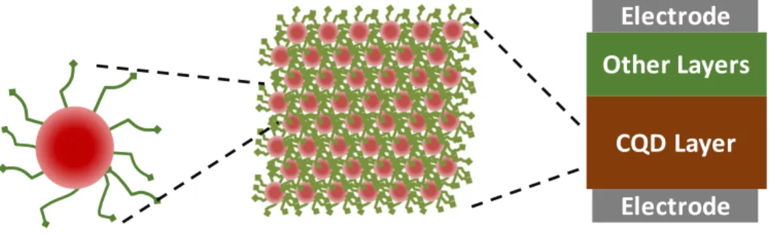
Colloidal quantum dots (CQDs) are zero-dimensional semiconductor materials that show strong quantum confinement effects. [23] When a electron is excited into con-duction bands, it leaves a positive charge (hole) then they make an electron-hole pair, an exciton. An exciton Bohr radius defines a size of the electron-hole pair in the similar logic with a distance between an electron and a proton in a hydrogen atom. When a size of materials becomes smaller than the exciton Bohr radius, electronic and optical properties of the materials are significantly affected by their size. Be-cause of the size-dependent unique optical and electrical properties of CQDs, they have recently been investigated as materials for next-generation optoelectronic de-vices, where the fact that they provide extremely high tunability in their optical and electronic properties presents an exciting opportunity. Specifically, control over the CQD energy gap, relative energy levels, and optical absorption, combined with their low-temperature solution processability and high stability makes them appealing as candidate materials for the solar cell active layer.
CQD Layer
Electrode
Other Layers
Electrode
Figure 1-2: A CQD structure: semiconductor cores and ligands attached to the cores (left). CQDs are used as a form of layers in the optoelectronic devices (right).
The energy gap between the highest occupied molecular orbital (HOMO) and the lowest unoccupied molecular orbital (LUMO) of CQDs is determined by their size when the radius of the CQD is smaller than the bulk exciton Bohr radius. Therefore, as shown in Figure 1-1, [1] one can tune the optical properties of CQDs by simply changing their size, which is extremely powerful for designing tailored optical absorp-tion in solar cells, especially in the case of multi-juncabsorp-tion tandem structures. [10, 24] Furthermore, in nearly all large-scale processing approaches to CQD layers, ligand molecules used during the synthesis to control growth, will remain attached to the surface of the CQD even after deposited as a layer in a film (see Figure 1-2). While these ligands play critical roles in stabilizing the deposition process and in passivating the surface trap states, they can shift the CQDs energy levels considerably. [17] For example, as reported in Ref. [25], where the scanning tunneling spectroscopy were used to measure the density of states of CQDs with different ligands, simple ligand exchange from trioctylphosphine ligands to aniline ligands, changes the band levels of the CQDs by ⇠0.3eV , which is larger than desirable in order to have good control over charge transport at interfaces between CQD layers and adjacent functional layers
Spin-coating
Contact-printing
Dip-coating
Electrophoresis
(a) (b)
(c) (d)
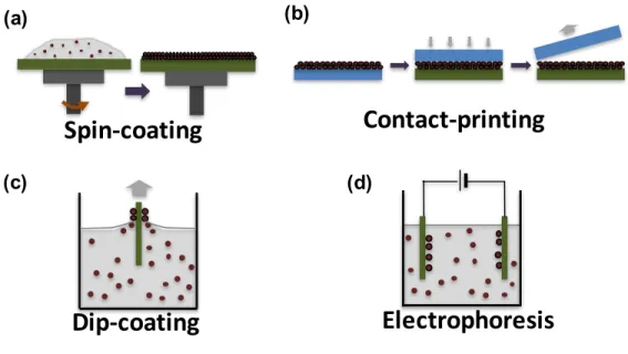
Figure 1-3: Common CQD solid deposition methods: (a) spin-coating, (b) contact(or transfer) printing, (c) dip-coating, and (d) electrophoresis.
in the solar cells. In lead sulfide (PbS) CQDs, which is most commonly used CQD materials for solar cells, up to 0.9eV energy level shifts were recently observed from ultraviolet photoelectron spectroscopy. [26]
In addition to the potential advantages of optical and electronic tunability, CQDs also provide advantages in solar cell device fabrication. Since CQDs are synthesized via solution processing, it is possible to apply wet-processes in the manufacturing of the solar cells, such as spin-coating, [13,27] dip-coating, [28] contact printing, [29,30] and electrophoresis [31] as shown in Figure 1-3. These solution-based processes are not only cheaper than vacuum-based device fabrication, but effective for building complex geometries. Moreover, CQD-based solar cells can show a high degree of robustness in air that is major challenge in polymer-based and perovskite solar cells, since the air-sensitivity of CQDs can be decreased using strongly bound ligands without sig-nificant degradation in optical properties [32] and solar cell performances. [15] This robustness enables the potential for encapsulation-free solar cells based on CQD lay-ers, which would be favorable for further cost-reduction.
1.2 CQD based solar cells
CQD based solar cells have been intensively studied and developed since the mid 2000s. Despite such a relatively short history, the best performance of CQD-based so-lar cells has already surpassed 10% in power conversion efficiently (PCE). [33] Among CQDs used for solar cells, PbS has been investigated actively because of its broadband optical response; the optical spectra of PbS CQDs can covers a broad range of so-lar light spectrum from a collection of different sizes, including far-infrared, especially when compared with leading absorber materials in organic (P3HT) [34] and inorganic (Si) [35] solar cells which only cover a much smaller part of the visible spectrum. Although the PCE of CQD based solar cells has shown remarkable improvement for last 10 years (from 1.3% [36] to the current 10% [33]), this value is still to low for CQDs to be appealing in commercial applications. The dominant discrepancy between CQD solar cells being able to take full advantage of the major benefits described above, and the still-low device performance achieved thus far, can be attributed to the low carrier mobility in CQD active layers. The reported charge carrier mobility in PbS CQDs for both electrons and holes covers a broad range, from 10 4 to 10 2cm2/(V.s), [12,14,20]
much smaller than that of other conductive materials (see Table 1.1). The reason for the low charge carrier mobility in CQD solids is their slow transport kinetics: hopping transport.
Not only does the low charge carrier mobility degrade the charge extraction ability in the CQD solar cells, but it also limits the thickness of the light absorption layer. A diffusion length of charge carriers can be determined from mobility. For example, if mobility become lower, the diffusion length decreases. If light absorption layers in solar cells are thicker than the charge diffusion lengths, charges will be recombined before they reach electrodes where they are collected as currents, degrading solar cell performance. The reported CQD solar cells still have thin CQD layers about 200nm, [15, 33] which is not sufficient to fully absorb sunlight; in fact, more than
Table 1.1: Charge Carrier Mobility of Conductive Materials (cm2/(V ·s))
Materials Electron Mobility Hole Mobility
Si [38] ⇠2⇥103 ⇠5⇥102 GaAs [38] ⇠7⇥103 ⇠4⇥102 P3HT [39] ⇠1⇥10 2 PbS (bulk) [40, 41] 7⇥102 2.2⇠12.8 PbS (CQD) [12, 14, 20] 1.6⇥10 4⇠4⇥10 2 1.5⇥10 3 CdSe (bulk) [42] 7.2⇥102 75 CdSe (CQD) [43, 44] 3⇥10 2⇠16 1000nm is required. [37]
1.2.1 Principal of operation
The best performance in CQD based solar cells was achieved using a heterojunction architecture. [33] Figure 1-4 shows the energy diagram of the heterojunction PbS CQD solar cells with a ZnO electron transport layer (ETL). When CQD layers ab-sorb sun-light, electron-hole pairs are generated. The electron-hole pairs either make the charge carriers, electrons and holes, or diffuse in a form of bound electron-hole (excitons). While electrons transfer into the electron transport layer, holes are col-lected in the opposite electrode. Exciton diffusions and dissociation processes can also happen; in this case the dissociation mainly happens at the heterojunction interface. Architecture of solar cells and their photovoltaic performance significantly depend on how quickly the dissociation process can occur. In the case of solar cells based on the organic materials, for example, excitons are dissociated mostly at the heterojunction due to the strong exciton binding energy, leading to the limitation on the absorption layer thickness (under the exciton diffusion lengths).
ETL
CQDs
Light
-
+
e
h
Figure 1-4: A schematic of heterojunction solar cells. The generated charges from the light absorption transfers to opposite directions. While the heterojunction can block the hole transfer and also accelerate the exciton dissociation, electrons transfer to the electron transport layer (ETL).
!60$ 140$ 340$ 540$ 740$ 940$ !1$ 0$ 1$ 2$ 3$ 4$
V
V
OCJ
SCJ
P
maxV
maxJ
maxFigure 1-5: A typical J-V curve of solar cells; the red line indicate the J-V curve where the short-circuit current (JSC) and the open-circuit voltage (VOC) are marked. The
violet line shows the power generated from the J-V curves; Jmax and Vmax indicate
the current density and the voltages when the maximum power can be achieved. The efficiency of solar cells is estimated based on how much power they can produce under the solar light; in fact, simple measurements of electric current at applied bias under illumination can provide such information. A typical current vs. voltage (J-V) curve of solar cells is given in Figure 1-5. The short-circuit current marked as JSC
indicates how effective the generated charges can be extracted at the electrodes while the open-circuit voltages marked as VOC defines the maximum differences in chemical
potentials of electrons and holes. The power conversion efficiency (PCE) is measured at the maximum power point using the relation:
P.C.E = JSC⇥VOC⇥F F
P0 (1.1)
where F F is the fill factor defined by the ratio of the maximum operating power to the theoretical maximum power, JSC⇥VOC, and P0 is the incident solar energy per
second.
case and the net current becomes zero at the open-circuit state where the energy gap between quasi Fermi levels (chemical potentials of electrons and holes) limits the VOC.
Large generation rates and high doping levels can increase the VOC by increasing the
energy gap, whereas the high charge carrier mobility and the slow recombination of electron-hole pairs are required to enhance the JSC.
1.3 Objectives
1.3.1 Design of CQD solids
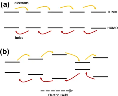
Since CQD solids consist of individual CQDs which may have dispersion in their material properties such as sizes, ligand coverages, stoichiometry, and/or shapes, the optical and electrical behavior of CQD solids is measured as an ensemble of those individual properties. Furthermore, the randomly close-packed CQD arrangements in commonly used CQD solids place the localized energy states in a range of posi-tions, causing the inhomogeneity in the interactions among CQDs. In addition to the slow kinetics in charge hopping transport, those disorders in CQD solids can disrupt the transfer of the charges, reducing the charge carrier mobility. In particular, the size-dispersion in CQDs prepared from solution-based processes can change both the energetic structures and the positions, which may alter charge transport behaviors. As shown in Figure 1-6, charge transport in CQD solids with size-dispersion com-pletely differs from that in monodisperse CQD solids. In other words, design of the architecture and morphology of CQD solids can play a critical role in controlling the charge carrier mobility and in enhancing the device performances.
1.3.2 Flow of thesis
In this thesis, we analyze the charge transport in CQD solids in terms of their design factors, such as polydispersity and periodicity, using a hopping transport code we have developed from scratch. After we introduce the details of the computational
(a)
(b)
Electric Field electrons holes LUMO HOMOFigure 1-6: Charge carrier transport in (a) monodisperse and (b) polydisperse CQD solids. Electrons (yellow) and holes (red) transfer in opposite directions with respect to applied electric field. The charge transport rates become dissonant when there are inhomogeneities in inter-CQD distance and the electronic energy structures, which leads to slower charge carrier transport.
methods in Chapter 2, out results related to the impact of size-dispersion on charge carrier mobility and the photovoltaic performance will be presented in Chapter 3. In Chapter 4, we suggest design rules and strategies for higher charge carrier mobility in CQD solids, combined with predictions of enhanced photovoltaic performances from such strategies. In Chapter 5, we extend the CQD design strategies to further ideas involving the use of binary CQD solids, which we expect to increase optical absorption and charge transport.
Chapter 2
Methods
While a wide range of theoretical approaches have been employed to understand charge transport phenomena in CQD solids, systematic studies related to the impact of CQD designs in terms of their size have been lacking. This is not only because there is no effective method to trace the individual charge transport rates between CQD pairs, but also because experimental controls on CQD sizes are still extremely cumbersome. Therefore, computational studies of the behavior of charge carriers are essential in order to better understand the transport properties of CQD solids. Moreover, for a complicated system such as a CQD film with inhomogeneity, in which a number of different processes can occur simultaneously, computational approaches provide the ability to separate the role and impact of each process, providing a much deeper understanding of the overall mechanism.
This chapter is written partially based on the published paper: Sangjin Lee, David Zhitomirsky, and Jeffrey, C. Grossman. Manipulating Electronic Energy Disorder in Colloidal Quantum Dot Solids for Enhanced Charge Carrier Transport. Adv. Func. Mat., 26:1154-1562, 2016
2.1 Charge Transport in CQD solids
CQD solids have been simulated using bulk semiconductor models for the sake of convenience, using existing measurement methods available for various optoelectronic devices; in fact, the reported charge carrier mobilities of CQD solids were obtained from time-of-flight analysis [14] or field-effect-transistor measurements [3], then the measured mobility is used for describing CQD solids. However, in contrast to bulk semiconductor materials, the electron wavefunctions of each individual CQD are usu-ally localized due to the ligands attached to it and the inter-dot distances, causing completely different charge transport mechanism, specifically hopping transport. Electron hopping transport has been also studied in other systems with localized en-ergy states such as organic semiconductors [45–47] and molecular junctions. [48–50] In contrast to resonant charge transport with strong wavefunction coupling that can be usually found in bulk semiconductor materials, hopping transport requires the assis-tance of phonons that activate the electrons as they can jump to other CQDs through the energy barriers in the middle of two separated electron states. [51] A simple form of hopping transport equation was suggested by Miller and Abraham, [52] where an exponential form of thermal activation energy was used to define the assistance from phonons. More detailed theory, including coupling energies (overlap integrals between the wavefunctions of a donor and an acceptor) and reorganization energies from the different charge distribution between before and after the transition, was developed later by Marcus. [53] A few studies have built numerical simulation models for pre-dicting transport in a system comprised of localized energy states using mainly two computing methods: direct solution of master-equations [54–58] and kinetic Monte Carlo simulations. [59, 60] The former includes hopping transport rates between the localized energy states and the probability of occupancies (charge density) for the energy states in the equations, which are usually the form of continuity equations for charge carriers, then finds the equilibrium occupancy of charges in each CQD. On the other hand, kinetic Monte Carlo simulations estimate how individual charges behave for each time interval, during which all the processes including recombination,
gener-ation, and transport that occur at randomized probabilities are taken into account. Kinetic Monte Carlo simulations can provide time-dependent information since all the behaviors of charges are recorded but a larger amount of computing resource is required, whereas direct solution of master-equations usually estimate the system in equilibrium within less computation time. While kinetic Monte Carlo can provide accurate simulation as long as all the processes are properly defined since it directly mimics the actual processes, direct solution of master-equations are knowns to be comparable to kinetic Monte Carlo as long as the processes involved are defined in the same manner and the short-term Coulomb interactions are negligible. [61]
2.2 Theoretical background
In order to compute charge transport in CQD solids, we adopt an approach based on the direct solution of master-equations since 1) handling large amounts of samples (more than 5,000 samples) which is required to statistically analyze the inhomogeneity such as polydispersity, demands very large computing resources and calls for short simulation times, [62] 2) thin CQD film thickness along the electric fields may not guarantee enough numbers of states to equilibrate the overall charge transfer in the kinetic Monte Carlo, and 3) describing the charge transport rates between CQDs and electrodes (or bulk semiconductors) becomes easier in the method with direct solution of master-equations; see 2.2.3 for the details.
2.2.1 Charge hopping transport
In order to construct the equations to solve, hopping transport rates between two CQDs have to be defined. Based on the Miller-Abraham hopping equation, [52] the charge transport rate from a donor CQD to an acceptor CQD is defined:
rD!A = NDVAHfexp ✓ d ↵D d ↵A ED!A+| ED!A| 2kT ◆ (2.1) where rD!A is the hopping transport rate from a donor to an acceptor, Hf is the
hopping frequency, ND is the number of charges in the donor CQD, VA is the ratio of
empty states for the charge in the acceptor CQD, ↵D and ↵Arepresent the localization
lengths of donor and acceptor CQDs, respectively, which is set to be comparable to their radii, [63] d is the center-to-center distance between acceptor and donor CQDs, and ED!A is the energy difference when the charge transports from the donor to
the acceptor. While the localization lengths can vary between CQDs, these changes can be absorbed into the hopping frequency coefficient, Hf, because we assume no
enhancement or degradation of interactions in specific CQD pairs, or between a CQD and ligands, exists. This model implies that the charges need thermal activation in order to tunnel through the distance d from lower energy levels to higher energy levels; no extra energy is required to hop from higher energy levels to lower energy levels, leading to a negative ED!A and zero thermal activation energy. Note that
the charge hopping transport defined by this equations is not limited to neighboring CQD pairs, employing the variable-range-hopping (VRH) mechanism [63, 64] where charge can jump to distant states with lower energy barriers rather than a nearest site with higher energy barriers.
2.2.2 Equations
Figure 2-1 shows an example of the CQD solid unit cell. For all CQDs in the simula-tion unit cell, our hopping transport simulasimula-tions solve for equilibrium in the charge continuity equations:
dN
dt = Gext Unet+ Re,in Re,out (2.2) dP
dt = Gext Unet+ Rh,in Rh,out (2.3) where N(P ) is the number of electrons (holes) in each CQD, Gext is the
exter-nal generation rate, Unet is the net recombination rate, Re,in(Rh,in) is the incoming
rate of electrons (holes) from nearby CQDs within a predefined cut-off distance, and Re,out(Rh,out) is the outgoing rate of electrons (holes) into the nearby CQDs within
Figure 2-1: An example of CQD film unit cell for a hopping transport simulation (left); two electrodes are set at the top and bottom of the unit cell (right) and the electric fields are applied in the +z-direction.
the same pre-defined cut-off distance; charge transport complies with the VRH mech-anism, where transport is not limited to the nearest hopping sites, especially for the highly disordered cases. Periodic boundary conditions are employed for the x and y directions (see Figure 2-1). Each CQD-to-CQD charge transport rate was defined based on equation 2.1.
In addition, electric potentials of the CQDs, determining the shift of energy levels, are estimated based on:
=
Z zCQD
zmax
~
E(z)dz (2.4)
where zCQD is the z-coordinate of the CQD, zmax is the maximum z-coordinate
of the CQD simulation unit cell (the position of ground electrodes), and ~E(z) is the electric field estimated at each z point with the same x and y coordinates as the CQD, using all other CQDs’ net charge and the applied electric field.
2.2.3 Boundary conditions
While periodic boundary conditions work horizontally (x and y directions), addi-tional boundary conditions at z = 0 and z = zmaxat the positions of the electrodes are
required; since most CQD-based optoelectronic devices usually involve CQD solids as a thin film, periodic boundary conditions at these edges cannot model the actual device working. Rather, charge flows at those boundaries should be estimated with all transport rates from and to the nearby CQDs taken into account. Although there are mainly two simple types of boundary conditions widely used solely or together for charge transport simulations [65,66] (Neumann conditions with fixed flows or Dirich-let boundary conditions with fixed charge densities), neither of these conditions can be incorporated easily into our simulation because 1) the current density at the elec-trodes should be estimated instead of being fixed, 2) the information on the effective number of charge at the electrode is lacking, and 3) an accurate behavior of individual charge transfer between electrode and CQDs is difficult to obtain either experimen-tally or theoretically. Therefore, we set the boundary conditions at the electrodes by comparing the equilibrium energy levels as described in Figure 2-2.
The chemical potential of electrons, for example, can be determined in CQDs near the electrodes using their electron occupancies, which is shown as dashed line A in Figure 2-2(a). When the Fermi level of the metal electrodes is at the same level with the electron chemical potential of the CQD, the net electron transport becomes zero, meaning equilibrium. In the case where the chemical potential of electrons in the CQD lies in unbalanced positions with the Fermi level of the metal electrode, such as the dashed line B, a larger amount of electron flow occurs into the CQD (L) than from the CQD (R), giving an overall net electron flux into the CQD. In our simu-lation, we calculate the electron flow from the electrode (L), based on the electron transport rate from the CQD to the electrode using the number of electrons assuming the electron chemical potential is placed in balanced with the electrodes (the dashed line C). While this method does not require knowledge of the detailed behavior of charges and the transport probability, which is essential for kinetic Monte Carlo
sim-HOMO
LUMO
A
E
FB
HOMO
LUMO
C
E
FL
R
(a)
(b)
Figure 2-2: Boundary conditions in the hopping transport code: (a) at equilibrium, the chemical potential of the charge (electrons in this case) lies in balance with the Fermi level of the electrode, and (b) the electron transport rates from the electrode to the CQD LUMO level (L) become larger than the rate in the opposite way (R) until the net charge transfer become zero. The larger rate (L) increases the number of electrons in the CQD LUMO level, pushing the chemical potential from B to C which is in balance with the Fermi level of the electrode. The transport rate (L) is defined as the balanced transport rate with the charge transport rate from the CQD LUMO level to the electrode assuming the electron chemical potential is in the level C. This definition does not require the detailed information in charge density in the electrodes and in the form of transport rates between the CQD and the electrodes.
ulations, the current density into/from the CQD solids can be easily estimated using the number of charges and the electric potentials of the CQDs, which are variables we solve for in our approach. Note that in the case of Figure 2-2, this method allows the incoming electrons from the electrodes (L) to keep flowing until the number of electrons in the CQD reaches the balanced electric potentials.
2.3 Flow of simulations
Figure 2-3 shows the overall flow of our CQD charge transport simulation approach. We input each CQD’s information including a coordinate, energy levels and, if neces-sary, a doping level. Doping levels of CQDs are used for solar cell simulations where the number of ionized dopants are directly defined for each CQD. The external gener-ation rates are also able to be included when we simulate the CQD solar cells device performance. A multivariable Newton method [67] is adopted to solve the equations 2.2, 2.3, and 2.4 under a given external electric field. For each CQD, there are three variables (Ni, Pi, and i) updated at each step using Jacobian Matrix:
0 B B B B B B B B B B B B B B B B B B B B B @ N1 P1 1 N2 P2 2 ... ... ... 1 C C C C C C C C C C C C C C C C C C C C C A = 0 B B B B B B B B B B B B B B B B B B B B B @ @FN1 @N1 @FN1 @P1 @FN1 @ 1 @FN1 @N2 @FN1 @P2 @FN1 @ 2 @FP1 @N1 @FP1 @P1 @FP1 @ 1 @FP1 @N2 @FP1 @P2 @FP1 @ 2 · · · · @F 1 @N1 @F 1 @P1 @F 1 @ 1 @F 1 @N2 @F 1 @P2 @F 1 @ 2 @FN2 @N1 @FN2 @P1 @FN2 @ 1 @FN2 @N2 @FN2 @P2 @FN2 @ 2 @FP2 @N1 @FP2 @P1 @FP2 @ 1 @FP2 @N2 @FP2 @P2 @FP2 @ 2 · · · · @F 2 @N1 @F 2 @P1 @F 2 @ 1 @F 2 @N2 @F 2 @P2 @F 2 @ 2 ... ... ... ... ... ... ... 1 C C C C C C C C C C C C C C C C C C C C C A 10 B B B B B B B B B B B B B B B B B B B B B @ FN1 FP1 F 1 FN2 FP2 F 2 ... ... ... 1 C C C C C C C C C C C C C C C C C C C C C A (2.5) where FNi and FPi are the right side of the charge continuity equations 2.2 and 2.3,
Start
Load CQD information Define computing conditions
Update the variables (N, P and φ)
Calculate Jacobian matrix Calculate FN, FP, Fφ Save Results Estimate ΔN, ΔP and Δφ Finish Converged enough?
Y
N
Figure 2-3: The flow chart of the hopping transport simulation code; using the mul-tivariable Newton method, the code computes the number of charges and the electric potential for each CQD in equilibrium based on the loaded CQD information on their positions and the electronic structures.
by equation 2.4; F i ⌘ i = i Z zi zmax ~ E(z)dz (2.6)
The computation loop in Figure 2-3 keeps running until the variables and the cur-rent density converges under a pre-defined relative tolerance (10 8). In addition to
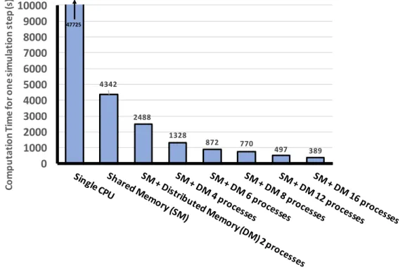
the convergence tests carried out for the unit cell sizes in order to exclude finite size effects from the periodic boundary conditions, the cut-off distance for the hopping transport rates was taken to be long enough to include all possible transport pairs. The computation code includes hybrid parallelizations using both the shared-memory and distributed-memory parallelization. In the shared-memory parallelization, the computing cores (central processing units, CPUs) can access the shared memory quickly but the number of available cores has a limitation from the computer archi-tecture, while the distributed-memory parallelization uses many number of systems, which are easily added to expand computing resource, communicating one another (slower than the shared-memory parallelization) in order to send and receive data computed separately in individual systems. Considering the large amount of com-putational samples for statistical analysis of the effects of inhomogeneity in CQD systems demanding significant computing resources even if we use the relatively sim-ple direct solution of master-equation method, extensive parallelization is essential for obtaining results within a reasonable time; in fact, the actual computation time was reduced by more than 100 times as shown in Figure 2-4 where the computation time for one step of the computation loop, including Jacobian matrix inversion (gaussian elimination) and integrating on the electric field, with respect to the level of paral-lelization is plotted.
2.3.1 Major assumptions
We note that the variables in equation 2.1 are time-averaged in the equilibrium of the charge continuity equations (2.2 and 2.3); for example, ND is allowed to be a
non-47725 4342 2488 1328 872 770 497 389 0 1000 2000 3000 4000 5000 6000 7000 8000 9000 10000 Co m pu ta tio n Ti m e fo r o ne si m ul at io n st ep (s )
Figure 2-4: Computing times for one step in the loop of the hopping transport code with respect to the level of parallelization. The number of process indicates how many nodes were used for distributed memory (DM) parallelization, where each node run a single process at shared memory (SM) parallelization. A single-core process takes 120 times longer than extensive the hybrid parallelization cases.
integer. Although non-integer numbers for charge can significantly underestimate charge-to-charge interactions such as the Efros-Shklovskii Variable Range Hopping (ES-VRH) at low temperature, ES-VRH is known not to be dominant in the temper-ature used in out simulations (300K); [68, 69]
The localization lengths of CQDs are set to their radii of them under the assump-tion that the electron wavefuncassump-tions are confined inside the CQDs. While there can be some modifications in localization lengths from the local charging energies and electrostatic potential, we assume that such effects are negligible because 1) the av-erage number of charges for CQDs in equilibrium were found to be very small, and 2) applied electric fields from computing the charge carrier mobility were found to be much higher than the local electric fields induced by those small numbers of charges, adding negligible gradients in the electric potentials of CQDs in the applied electric field direction, which presumably leads to no significant changes in overlap integrals of the wavefunctions in the electric field directions despite the asymmetry in the indi-vidual wavefunction. Recent reports showed that the localization lengths may change dramatically as a function of doping of the CQDs but the critical doping level is sig-nificantly higher (more than 10 electrons or holes per CQD) than the value we used in our simulation of photovoltaic performance estimation (10 4 hole per CQD). [70]
We did not include charging effect in estimating charge hopping rates. While the exact charging energies are quite difficult to address in our simulation because of the time-averaged non-integer number of charges, it has been reported that the charging energy usually increased when nanoparticle size decreases. [71] This size-dependent charging energy can actually intensify the site-energy dispersions in the polydisperse CQD films.
We used the HOMO and LUMO levels as effective charge transport paths. Involve-ment of higher energy levels (for example, the second lowest occupied levels and the second highest unoccupied levels) can increase the charge carrier mobility of CQD films by providing additional states available for charge transfer. However, as shown in Figure 2-5, we confirmed that such effects disappears when the energy difference between the first and second energy levels is larger than 150meV, as is the case for
0
0.05
0.1
0.15
0.2
0.25
0.3
0.35
0
0.1
0.2
Mo
bi
lit
y
(c
m
2/V
s)
Energy Separation (eV)
Figure 2-5: Trend in electron mobility when the 2nd lowest unoccupied energy levels are included into the simulation; we confirmed that the second levels can be ignored when the separation between LUMO levels and the 2nd lowest unoccupied energy levels is larger than 0.15eV, where differences from the LUMO-only electron mobility become lower than 0.1%.
the range of PbS CQD sizes we are interested in (under 3nm in radius). [1, 4]
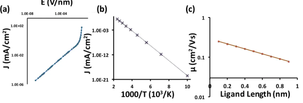
2.4 Validity test
The computed electric transport characteristics of the CQD solids showed trends in good agreement with experimental measurements of the field-dependence of conduc-tance [2] (Figure 2-6(a)), temperature dependence of conducconduc-tance [2] (Figure 2-6(b)), and exponentially increasing mobility with decreasing ligand length [3] (Figure 2-6(c)). The conductivity and the mobility in these experiments were estimated using FET measurements. While the agreements in trends between our simulation results and the experimental measurement can guarantee that the systems are in the same charge transport regime, the numbers such as current densities, mobility, or conduc-tances, differ from each other because the detailed experiment conditions cannot be taken into account in the simulation; instead, we use the hopping frequency, Hf in
1.0E%06' 1.0E%02' 1.0E+02'
1.0E%08' 1.0E%04' 1.0E+00'
J(m A /c m 2) E (V/nm) 1.0E%21' 1.0E%12' 1.0E%03' 2' 4' 6' 8' 10' J(m A /c m 2) 1000/T (103/K) 0.01$ 0.1$ 1$ 0$ 0.2$ 0.4$ 0.6$ 0.8$ 1$ μ (c m 2 /V . s) Ligand Length (nm) (a) (b) (c)
Figure 2-6: Simulation results that show good agreement with the data from ex-perimental measurements: (a) electric field dependency of the current density for closed-packed CQD solids. Current density shows the similar trends to the exper-imental measurement including ohmic to non-ohmic transitions at the high electric field (Ref [2]), (b)The computed temperature dependency of the current density for close-packed CQD solids in good agreement with experimental trends in Ref [2], and (c) The computed trends in charge carrier mobility with respect to the ligand lengths; exponential increases in charge carrier mobility with decreasing ligand lengths show a good agreement with the measured mobilities in Ref [3].
equation 2.1, which can be relatively tuned with respect to the conditions we want to investigate. While the agreed trends in the field-dependence of conductance confirm that the equation 2.1 simulates the experiment well in terms of how the site energy difference reduces the charge transport, the same trends in temperature dependence of conductance between the simulations and the experiments verify that thermal ac-tivation process is well defined in our code and the simulated CQD systems have no strong charge-to-charge interactions. The exponential decay of mobility with in-creasing ligand lengths, which is also observed from the experiments, supports that overlaps between localized wave functions are well described with the exponential form for the center-to-center distances and the localization lengths in the equation 2.1.
Chapter 3
Polydispersity in CQD solids
Although CQD solids have been widely applied in optoelectronic devices taking ad-vantage of their unique optical properties, as mentioned in Chapter 1 such applications have been limited by the relative low charge carrier mobility of CQD films. Polydis-persity introduced to the CQD solids has been believed to significantly degrade the charge transport throughout the film since energetic and spatial disorders cause in-homogeneity in the hopping transport. In this chapter, the impact of this electronic energy disorder originating from the size dispersion of CQDs on the charge carrier mobility in CQD solids will be analyzed. Then, we will show how the CQD solar cells performance is affected by size-dispersion.
This chapter is written partially based on the published paper: Sangjin Lee, David Zhitomirsky, and Jeffrey, C. Grossman. Manipulating Electronic Energy Disorder in Colloidal Quantum Dot Solids for Enhanced Charge Carrier Transport. Adv. Func. Mat., 26:1154-1562, 2016
3.1 Low Mobility in CQD Solids
As we have already discussed, the relatively low charge carrier mobility (0.0001-0.01cm2V 1s 1) [12, 20, 72] in CQD active layers originates from the fact that the
charge carrier transport depends mainly on slow kinetics, namely vis a hopping trans-port mechanism. [51, 73] A number of studies have explored ways to enhance the carrier mobility in CQD layers, including the use of shorter ligands, [3] reduction of trap density by surface passivation, [74,75] alignment of energy levels with ligands for nearly resonant transport, [76] and induction of band-like transport; [44] in some cases charge carrier mobilities higher than 10cm2V 1s 1 have been achieved. [77–80] Size
dispersion in as-synthesized CQDs is considered another source of mobility loss and device performance degradation. CQDs synthesized from conventional wet-chemistry processes possess a 5%-15% size dispersion, [3,81,82] causing a corresponding disper-sion in the energy gaps between the HOMO and LUMO of the individual CQDs. This inhomogeneity in electronic energy levels can disrupt the charge hopping transport in CQD films and degrade the transport rate significantly. In addition, a sufficiently narrow CQD size dispersion is essential to achieve the periodic super-crystals that have shown dramatic enhancement in carrier mobility in CQD field effect transistors due to the reduced inter-particle spacing and increased exchange coupling from the ligand treatment. [83] The impact of CQD size dispersion on the charge carrier mobil-ity in CQD films is little understood, and apparently contradictory results such as a lack of correlation between polydispersity and carrier mobility [3,59] versus the high carrier mobility observed using monodisperse CQDs, [83] calls for further investiga-tion into the impact of radius distribuinvestiga-tion of CQDs on the carrier mobility in CQD films. Furthermore, while recent work showed that CQD solar cell performance was not influenced by polydispersity since a high density of deep trap states degraded the charge transport in CQD active layers regardless of their size dispersion, [84] new concepts involving small ionic ligands and hybrid passivation strategies could suc-cessfully inactivate those trap states, [75] motivating the need for detailed studies on the impact of the CQD polydispersity, and for the establishment of design rules for
polydisperse CQD solids.
3.2 Impact of Polydispersity on Charge Carrier
Mo-bility
3.2.1 Preparation of CQD Solids
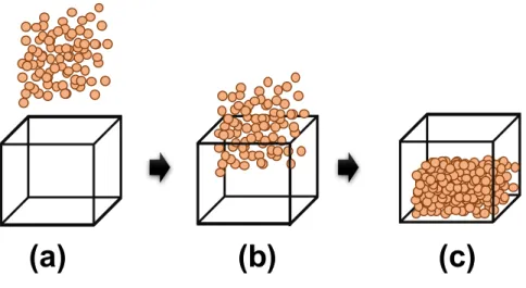
While a variety of CQD film deposition methods have been employed experimentally such as spin-casting, dip-coating, and electrophoresis, regardless of the technique the deposited films all possess randomly close-packed (RCP) CQD arrangements. [31, 77, 85] Thus, in our calculations we define the positions of CQDs in the RCP arrangement, via molecular dynamics (MD) simulations with spherical particles and a granular potential, mimicking the experimental CQD films deposition process. Figure 3-1 shows a schematic of the CQD solid preparations, where we adopted a two-step process: 1) place CQDs sparsely above the MD simulation box, then 2) start the MD simulation with a granular potential and an additional acceleration to force the particles into the simulation box. As discussed in Chapter 2, periodic boundary conditions are applied in the horizontal directions. The computations were carried out using the LAMMPS packages [86] where the granular potential adopted the Hookean styles described in Refs. [87–89]; the granular potential provides a strong repulsive force between two spheres only when they are overlapped with shorter inter-distances than the sum of their radii. After CQDs lose their energy from collisions, finally, the CQDs find their equilibrium positions as shown in Figure 3-1(c), which are then used in the hopping transport simulation code described in Chapter 2.
3.2.2 CQD solids with size-distribution
Computational samples of CQD films with 0%-15% size dispersions were prepared using MD simulations. Assuming each CQD with 4Å ligand length is a sphere, 1600 radii of CQDs were generated with a normal distribution with standard deviation ranging from 0 to 0.285 nm and an average radius of 1.9 nm. We refer to the bottom
(a)
(b)
(c)
Figure 3-1: A schematic of CQD film preparation for hopping transport simulations: (a) place CQD spheres sparsely above the MD simulation box, then sort them with respect to their size if necessary, (b) start MD simulations under the granular potential among CQD spheres and an additional downward acceleration, and (c) CQD spheres find their equilibrium positions.
of the simulation cell as the xy-plane (60 nm ⇥ 60 nm) located at z = 0 and the height of the cell corresponds to the z-axis (Figure 2-1). Generated CQD solids from the procedure described in the previous section have RCP configurations with packing density around 0.605, in good agreement with the reported results on the trend of core to total volume ratio with respect to the inter-CQD distance in the face-centered-cubic-like (FCC-like) amorphous phase. [90]
Next, positions and radii of CQDs were used to model charge transport where HOMO-LUMO gaps were calculated using a relation for lead sulfide (PbS) CQDs suggested by Moreels et al. [1], where d is the core diameter, and Eg is the HOMO-LUMO gap.
Eg = 0.41 +
1
0.0252d2+ 0.283d (3.1)
While the HOMO-LUMO gaps broaden as the CQD size decreases due to the quantum confinement effect, the changes in the individual energy levels are not symmetric. We therefore determined the HOMO and LUMO levels based directly on experimental
results from Hyun et al., [91] where the increases in LUMO levels with decreasing CQD size is larger than the decreases in HOMO levels.
The charge carrier mobility of CQD solids was estimated using the current density at 0.001 V nm 1 electric field, comparable to the electric field inside the depletion layer
in conventional CQD solar cells working at the maximum power point [37] or that between sources and drains in CQD field effect transistors, [44] and using the total number of carriers in the layers when all the charge continuity equations become close enough to zero so that the current densities converged to within 10 8 of the relative
tolerance. Note the charge carrier mobility estimated in this simulation includes contributions from all the charge distribution in the CQD solids and the internal electric field from the charge distribution since it is measured from external variables such as current density at the electrodes and the applied electric field.
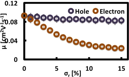
3.2.3 Impact of polydispersity on the charge transport
Figure 3-2 shows the trends of electron and hole mobility with increasing CQD size dispersion. 50 different samples were averaged for each size dispersion. Note that a 70% loss in the electron mobility is observed for samples with size dispersion around 10%. On the other hand, the hole mobility shows only a 11% decreases even in the most dispersive (15%) CQD radius distribution cases. This mobility reduction and the differences in electron and hole mobilities can be understood from the relation between spreads in site energy differences and the CQD size dispersion.
Figure 3-3 shows the increases in the standard deviations in neighboring site energy differences E between hopping pairs for all CQDs as the size dispersion broadens. Since the hopping transport equation 2.1 includes the energy difference terms inside the exponent, the variance in the neighboring site energy differences distracts the charge hopping transports into neighboring CQDs in terms of their directions and rates. The smaller reduction in the hole mobility can be attributed to the small increases in site energy deviation even for a large CQD size dispersion. We further tested this model to investigate the trends of charge carrier mobility in additional
tem-0
0.04
0.08
0.12
0
5
10
15
µ
[c
m
2V
-1s
-1]
σ
r[%]
Hole
Electron
Figure 3-2: Charge carrier mobility of CQD solids with respect to the polydispersity; the large drops are observed in electron mobility at 10-15% polydispersity while the hole mobility did not show significant reduction.
Figure 3-3: Standard deviations of site energy differences for each sample with respect to the dispersion in CQD ensemble; 50 samples were tested for each CQD size-dispersion.
Table 3.1: Electron mobility drops at 10% polydisperse CQD solids. Temperature Mean Radius Ligand Length Electron mobility drops
(K) (nm) (nm) at 10% polydispersity 200 1.9 0.4 87.7% 250 1.9 0.4 77.3% 350 1.9 0.4 57.1% 300 1.7 0.4 72.0% 300 2.1 0.4 61.8% 300 2.3 0.4 54.3% 300 1.9 0.2 62.0% 300 1.9 0.6 70.5% 300 1.9 0.8 73.4%
perature and mean size parameters; more than 54% of the electron mobility drops were observed from a wide variety of samples shown in Table 3.1.
The mobility drops become significant at low temperature, where not enough thermal energy is available for charges to overcome the energy barrier in polydis-perse CQD solids. VRH can provide other transport paths but the transport rates become significantly low due to the increased hopping distance. An increased mean radius makes the dispersion of site energy differences moderate, leading to less impact of polydispersity on the mobility drops. Longer ligands exponentially decrease the charge hopping transport rates in our model as expected from the equation 2.1, where d increases with longer ligands. Shorter ligands may provide more states available for charges to hop in shorter distance in the VRH regime, lowering the impact of