HAL Id: hal-01827055
https://hal.archives-ouvertes.fr/hal-01827055
Submitted on 1 Jul 2018
HAL is a multi-disciplinary open access
archive for the deposit and dissemination of
sci-entific research documents, whether they are
pub-lished or not. The documents may come from
teaching and research institutions in France or
abroad, or from public or private research centers.
L’archive ouverte pluridisciplinaire HAL, est
destinée au dépôt et à la diffusion de documents
scientifiques de niveau recherche, publiés ou non,
émanant des établissements d’enseignement et de
recherche français ou étrangers, des laboratoires
publics ou privés.
immune to device variations
Damien Querlioz, Olivier Bichler, Christian Gamrat
To cite this version:
Damien Querlioz, Olivier Bichler, Christian Gamrat. Simulation of a memristor-based spiking neural
network immune to device variations. 2011 International Joint Conference on Neural Networks (IJCNN
2011 - San Jose), Jul 2011, San Jose, United States. �10.1109/IJCNN.2011.6033439�. �hal-01827055�
Abstract— We propose a design methodology to exploit
adaptive nanodevices (memristors), virtually immune to their variability. Memristors are used as synapses in a spiking neural network performing unsupervised learning. The memristors learn through an adaptation of spike timing dependent plasticity. Neurons’ threshold is adjusted following a homeostasis-type rule. System level simulations on a textbook case show that performance can compare with traditional supervised networks of similar complexity. They also show the system can retain functionality with extreme variations of various memristors’ parameters, thanks to the robustness of the scheme, its unsupervised nature, and the power of homeostasis. Additionally the network can adjust to stimuli presented with different coding schemes.
I. INTRODUCTION
anotechnology has long been announced as a game changer of microelectronics. Nanodevices are compact, low power, and above all they provide novel functions like memristivity [1]. However, introducing them into actual products has proved challenging in particular due to their less desirable features: they have strong variability, and it is difficult to achieve acceptable yield. Fully exploiting nanoelectronics potential will thus require architectures and design approaches with an actual immunity to device variability and a high level of fault tolerance.
Spiking neural networks can provide a serious lead since the brain – in particular – itself relies on variable and unpredictable neurons and synapses [2] and manages computational efficiency that outperforms manmade systems. Architectures allying memristors synapses and CMOS neurons have been proposed [3]-[10], promising cognitive computing and robustness to defects. In this paper system simulations introduce quantitative results in terms of computing performances and robustness to variability. We show that a simplified spike timing dependent plasticity scheme adapted to memristors is key to achieve effective learning with extreme robustness to memristors’ variability. It is associated with the use of unsupervised learning, and of a homeostatic-type mechanism.
We describe the required technology and architecture (section II) and perform system-level simulations on the
Manuscript received February 10, 2011. This work was supported by the European Union through the FP7 Project NABAB (Contract FP7-216777).
D. Querlioz is with Institut d’Electronique Fondamentale, Univ. Paris-Sud, CNRS, 91405 Orsay, France (phone: +33 1 61 15 33 58; fax: +33 1 69 15 40 20; e-mail: damien.querlioz@u-psud.fr).
O. Bichler and C. Gamrat are with CEA, LIST, Embedded Computers Laboratory, 91191 Gif-sur-Yvette Cedex, France (e-mail: olivier.bichler@cea.fr, christian.gamrat@cea.fr)
MNIST database [11] that show the potential of the approach and its robustness. The system consists of a first fully unsupervised layer that extracts features of the inputs using a simplified spike timing dependent plasticity (section III), and can be complemented with a layer to label the outputs (section IV). The network performance compares favorably with traditional – but supervised networks with similar numbers of adjustable parameters and achieves excellent tolerance to various memristors’ parameters variability.
Technological context: In recent years several classes of
adaptive devices have emerged. The most famous are memristors [1] (stricto sensu memristive devices), resistive RAMs [12], or adaptive transistors like the NOMFETs [13] and OG-CNTFETs [14]. An emerging route is to exploit them as synapses in neuromorphic circuits (electronic circuits that work analogously to the brain). In particular it has been suggested [8],[9],[15], and shown experimentally [4], that such devices could indeed reproduce a feature of biological synapses – spike timing dependent plasticity (STDP) [16],[17] – that is believed to be a foundation for learning in the brain [18],[19]. A system consisting of nanoscale synapses and CMOS processing units (neurons) could be a major breakthrough in computing, possibly allowing cognitive-type tasks. This precise idea is currently receiving considerable interest through for example the DARPA SyNAPSE program in the USA or similar projects in Europe and Asia. However, its sustainability is still to be demonstrated.
As mentioned above, one common characteristic of all these technologies is a high degree of variability [20],[21]. Though technological maturity will improve the situation, it is expected to be intrinsic especially if we scale to ultra-small sizes that make the devices particularly sensitive to any variation in the fabrication process. This puts a challenge to designing systems able to exploit their new functionality. This paper provides some insight on how such technology may be exploited.
Prior art: Other proposals have been made to exploit
variable adaptive devices in the context of nanotechnological implementations. Most proposed architectures rely on reconfigurable logic (FPGA type) [22],[23] or on state-based supervised neural networks [7]. In the first approach variability is addressed through error mapping and redundancy, in the second case through a standard neural network approach using supervised learning based on error gradient descent.
Our approach of using unsupervised learning with asynchronous spiking neural networks to tackle the
Simulation of a Memristor-Based Spiking Neural Network
Immune to Device Variations
Damien Querlioz, Olivier Bichler and Christian Gamrat
variability issue of nanodevices is original and takes inspiration from recent works in computational neuroscience and neural networks [24]-[27]. Different works have been published that go into that direction. As mentioned above, several proposals exist to use memristive devices for STDP [8],[9],[15]. In this paper we propose a simplified STDP scheme that we believe to be easier to implement, and to allow learning in a more natural way. Additionally, we propose a homeostasic property to the neurons that has not been used in this context before and that is shown to be essential for the robustness of the scheme. One work had already shown that memristors with STDP could allow the emergence of receptive fields in a variability-compatible unsupervised approach and synchronous neurons [5]. Our work uses asynchronous designs (like the ones used in the neuromorphic community [28],[29]), and performs full learning on a standard dataset. Finally, an alternative way to allow learning with memristors in a variability-compatible way can be to use all digital designs [10]. This requires more devices per synapses [3]. In this paper we show that variation-tolerance can be retained by using nanodevices with continuous variation of the conductance.
II. PRESENTATION OF THE NETWORK AND OF ITS
IMPLEMENTATION A. Architecture
In this paper we first propose a simple two layer topology. Input and output CMOS neurons are connected in a feed-forward manner by nanodevices (the synapses), using a crossbar configuration (described below). The synapses learn using a simplified STDP scheme (II.B.1). The output neurons behave as leaky integrate-and-fire neurons (II.B.2) and have a homeostatic property (II.B.4). They are also connected by inhibitory connections using diffuser networks (II.B.3)
The input neurons present the stimuli as asynchronous voltage spikes using several possible coding schemes
described in section III (spiking rate is proportional to stimulus intensity). These stimuli may originate for example directly from a spiking retina [30] or cochlea [31] designed in the neuromorphic community. It is natural to lay out the nanodevices in the widely studied crossbar as illustrated on Fig. 1 (CMOS silicon neurons and their associated synaptic driving circuitry are the dots, the squares being the nanodevices). The synapses indeed act as adaptive resistors. With the crossbar layout, if several synapses are active at the same time (i.e. receiving spikes), the output receives directly the sum of the currents flowing through the synapses. In a more futuristic design, the system could also be laid out in a CMOL architecture where nanodevices crossbar is fabricated on top of the CMOS neurons and driving circuits [7].
As a result of learning, the output neurons will become selective to the different stimuli classes that are presented in a fully unsupervised manner: the output neurons will develop selectivity to specific features contained in the input patterns. The learning rule of the nanodevices needs to be fully local to be implementable in the crossbar architecture. The behavior of the neurons needs to be simple to make it easy to implement in a compact way. We now describe how this can be achieved.
B. Neurons and synapses
1) Synaptic behavior: In this scheme, the synapses are
acting in two ways. They are variable resistors and thus transmit spikes with a variable conductance (or weight). But
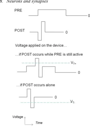
Fig. 2. Pulses for simplified STDP (voltage pulses as a function of time). When an input neuron spikes, it applies a PRE pulse to the nanodevices to which it is connected. When an output neuron spikes it applies a POST spike to the nanodevices to which it is connected. When the voltage applied on the device (difference between the voltages applied at the two ends) reaches VT+ or VT-, its conductance is increased or decreased, respectively.
Input layer 784 neurons (28*28)
Output layer
(integrate & fire neurons)
nanodevice
Fig. 1. Circuit topology. Wires originate from CMOS input layer (horizontal black wires) and from the CMOS output layer (vertical grey wires). Adaptive nanodevices are at the intersection of the horizontal and vertical wires.
they also adapt their weight depending on the activity of the neurons to which they are connected, which provides the foundation of learning by the system.
The memristive nanodevices are programmed as follows. When applied a positive voltage pulse higher than a threshold VT+, they increase their conductance. When
applied a voltage pulse smaller than a negative threshold VT-,
they decrease their conductance [4],[8]. Previous works have shown that memristors can implement spike timing dependent plasticity (STDP), a learning rule used by synapses in the brain. This was proposed in [9], itself close to the proposal [8] and experimentally demonstrated in [4]. We propose a simpler adaptation of these schemes (Fig. 2).
• When an input neuron spikes it applies a long pulse to its synapse (PRE pulse). This voltage is high enough to drive some current into the memristor but not enough to reprogram it. This current is integrated by the output neurons (resistor role of the synapse). If several synapses connected to the same output neuron are ON at the same time their currents are summed. • When an output neuron spikes it applies a pulse that is a
succession of a negative and a positive bias (POST pulse). If no PRE pulse is being applied on the device, only the second part reaches a threshold and the weight of the synapse is decreased by δw−. However, if the input neuron had spiked recently, and the PRE pulse is still being applied on the other end of the device, the voltage applied on the device actually increases its weight by δw+, as illustrated on
Fig. 2.
This simple learning rule, easily implemented with nanodevices, is the ground of all learning. Compared with the purely bioinspired and more complex scheme introduced in [9], no delay matching is necessary between the PRE and POST synaptic waveforms, which should make the driving circuitry much easier to design. The learning rule is also more appropriate for our feed-forward application.
The way this simple learning rule works is straightforward. When an output neuron declares a spike (at time tspike), it increases by δw+ the weights of the synapses
connected to input neurons that spiked recently (from tspike to
tspike-tPRE, if tPRE is the duration of the PRE pulse). It
decreases by δw− the weights of all its other synapses. This
increases the sensitivity of the neuron to the specific pattern that activated it, making it more likely to spike for a similar (correlated) pattern in the future. This process – that works surprisingly well in practice, as we show in this paper – has been partially theorized in [27].
To model the weight increments and decrements δw+ and
w
δ − in our system simulations, we take inspiration from the memristor measurements [4],[32]. When a POST occurs: if PRE has occurred just before the weight is increased by min max min w w w w w e β
δ
α
− + −− += + (1)in the other cases it is decreased by max max min w w w w w e β
δ
α
− − −− −= − (2)The exponential factor expresses the fact that is observed in most memrsitive technology that a same voltage pulse has reduced effect on the device conductance if applied several times [4],[32]. This natural (partly multiplicative) device behavior is actually a valuable behavior for learning. The parameters α+, α-, β+,β+ depend heavily on the PRE and POST pulse voltages that are chosen. These parameters, as well as minimum and maximum weights wmin and wmax are
subject to device variability.
2) Output neurons’ dynamics: Exploiting the devices
requires connecting them to processing units – silicon neurons able to process and generate spikes in a bioinspired manner by integration of their input. An approach widely studied in the neuromorphic community is to use analog circuits (generally with transistors operating in the sub-threshold regime) able to receive and generate asynchronous spikes [28],[29]. Though smaller than in nanodevices, variability is also a serious problem for such devices. It is a challenge for any neuromorphic design [31] and will become even more crucial when scaling to modern technology.
Neurons are leaky integrate-and-fire type that is meant to solve the simple equation (expressed in normalized unit): τdVdt +gV=Iinput (3)
where V is the state variable (a current or a voltage) of the neuron. Iinput is the current flowing through the line of the crossbar connected to the neuron:
=
∑
j j
input I
I (4)
where the Ij are the currents flowing through each memristor j connected to output neuron.
The neuron declares a spike if V reaches a given threshold
Vth, in which case V is reset to zero and the integration is prevented during a so-called refractory period.
Such neurons have been implemented with compact CMOS neuromorphic circuits as in [33] or equivalently with a neuromorphic circuit with positive feedback as in [28],[29].
This kind of CMOS design is extremely low power because most transistors operate in the subthreshold regime, and thanks to the use of asynchronous computation [28],[29]. On the other hand, power consumption of the nanosynapses will depend tremendously on the nanotechnology, and should scale with the devices.
3) Output neurons’ lateral inhibition: When an output
neuron spikes it should send inhibitory signals to the other output neurons of the layer that prevent them from spiking during the inhibition time and resets their potential to zero.
This inhibition between the neurons can be implemented in a compact way through diffuser networks as in [28]. With this inhibition, the network is reminiscent of a Winner-Takes-All topology [27].
More precisely, when an output neuron spikes, the state variable V of the other output neurons is reset to zero during a time tinhibit.
4) Homeostasis: A final difficulty for the architecture is
the adjustment of the neurons’ threshold. It is essential, but although this is natural for traditional artificial neuron networks, it is not for spiking neurons. A bioinspired original route is homoeostasis [2]. A target activity is defined for the neurons (i.e. a number of times an output neuron should spike over an extended period of time, like 100 digits presentation). Regularly the threshold of the neuron is increased if the average activity of the neuron is above the target, and decreased if it is below.
This ensures that all the outputs neurons are used and adjust the neurons’ thresholds to the stimuli for which they become specialized. In neuromorphic hardware, homoeostasis has been implemented with analog memories like in [34] or could be implemented digitally. The potential associated with this technology is evidenced in this paper in section III.B.
C. Simulations
In this paper, all simulations are system-level and are based on a C++ special purpose code. The code is event-based for simulation performance and runs on traditional CPUs. Simulation parameters as introduced above are τ = 100 ms, g = 1, Vth = 0.5 (normalized unit), inhibition
time tinhibit = 10 ms, α+ = 10-2, α− = 5.10-3, wmin = 10-4, max
w = 1 (normalized units), β+ = 3.0, β- = 3.0. The width of
the PRE pulses is 25 ms. Parameter variations are introduced around all the parameters using Gaussian random numbers (the value of their standard deviation is given in Section III). The initial weights are selected randomly around mid-range (0.5). The stimuli are applied using the coding schemes described in section III.C.
For demonstration of the concept, in this paper we use the widely studied case of handwritten number recognition. The
MNIST database is used, which consists in handwritten number of 28x28 pixels by 250 writers [11]. This database has been used as test for many learning algorithms.
In order to achieve learning, we present the full MNIST training database (60,000 digits) three times to the circuit. Each input neuron is connected with one pixel of the image. It emits spikes with a jittered rate that is proportional to the pixel intensity (maximum rate is 20 Hz). The initial phase is random. Every digit is presented during 350ms. No kind of preprocessing on the digits is used and the set is not augmented with distortions. The network is then tested on the MNIST test database (10,000 digits).
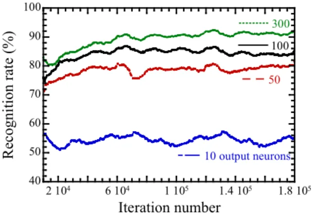
Fig. 3 plots the synaptic weights learned by the system in a configuration with only 10 output neurons. It is remarkable that without any supervision and using only our local custom STDP rule, the system has identified 9 (out of 10) different numbers, the real features of the input. Moreover it has learned the distinctive features of the digits (and not just the most likely handwriting): it has learnt the loop of the digit two, the bottom of the six, or the horizontal parts of three and eight.
In order to evaluate quantitatively the network performance, Fig. 4 plots the recognition rate during the learning process for different numbers of output neurons. To evaluate the recognition rate, we associate output neurons with the digit for which they spike the most frequently a
posteriori. In hardware this association could be performed
with digital circuitry. This labeling could also be implemented using nanodevices in a variability compatible way as will be shown in section IV.
With ten output neurons the recognition rate reaches 60 %. With 50 output neurons it reaches 81% and with 300 output neurons 93.5 % (obtained with the same number of adjustable weights). A traditional artificial neural network with back-propagation with 300 hidden neurons reaches 95 % [11], which compares to our rate of 93.5 %. In the literature, the best algorithm has a largely superior 99.7 %
40 50 60 70 80 90 100 2 104 6 104 1 105 1.4 105 1.8 105 100 10 output neurons 50 300 Recogni tion rat e (%) Iteration number
Fig. 4. Recognition rate during learning for simulations with different numbers of output neurons (from bottom to top: 10, 50, 100, 300). The recognition rates are running averages on 10,000 iterations.
Fig. 3. Weights (conductances) learned in a simulation with 10 output neurons. Red is maximum weight, blue is minimum weight.
recognition rate, but has 12 million adjustable weights (vs. 235,200 here) and is using a largely augmented training set [35]. Though our numbers are clearly more modest, the interest here is that the network is fully unsupervised with local extremely simple learning rules and variability immunity.
III. VARIABILITY IMMUNITY A. Synaptic variability
We first study the impact of nanodevices (synaptic) variability on the performance of the network. For this study, we simulated the network with 50 output neurons, introducing different kinds of variability. All the simulations were repeated five times, and the recognition rate given is averaged on the five runs. Simulation time was about 8 hours per run on an AMD Opteron 2216 CPU. Results are reported in Table I.
On the first row of Table I, we evaluate the impact of variability of the initial state (i.e. the initial weight of the nanodevices, before learning starts). We can see it has no impact on the final performance, even when the variability is extreme. This means that we do not need to control the initial weight precisely. This is fortunate since this would be extremely difficult with memristors.
On the second row of Table I, we evaluate the impact of the variations on the learning increments and decrements (α+, α−). These variations can be caused by variations of the
device thresholds and of their programming characteristics. We can see that the network is immune to variations up to 25% of the mean value of these parameters, which is already an extremely high level of variation for an electron device (but typical for research nanodevices). With 50% of variation, there is a small decrease of performance. With a dramatic variability of 100% on the synaptic parameters, the recognition rate decreases significantly, but interestingly the functionality of the network is not challenged. We should note that with a variability of 50%, 4% of the nanodevices cannot be programmed in at least one direction (i.e. they have an α value of 0). The latter figure becomes 30% when
parameter variability is 100%. This is an indication of the overall tolerance to defects.
The last row of Table I adds variations of
w
min, wmax. Inthat case some nanodevices will overpower the others due to increased maximum weight. Results are however similar to the previous case, and extreme robustness is preserved. The most sensitive parameter is the maximum weight.
Tolerance to synaptic variability is natural in a way since learning actually takes its root in synaptic variability. The degree of tolerance achieved is however still impressive.
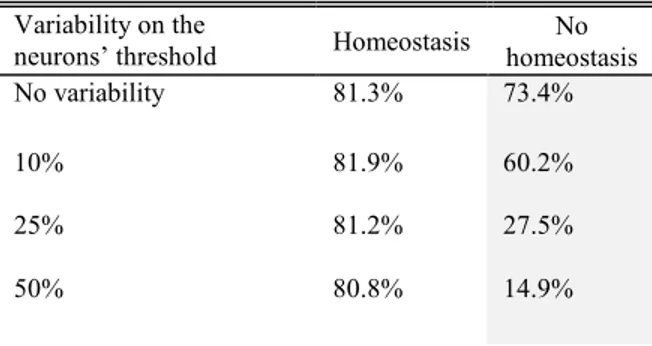
B. CMOS neuron variability
We now study the impact of the variability of the CMOS neurons. The impact of the variability of their threshold is seen in Table II. We can see that without homeostasis the impact of the variability is dramatic. The more excitable neurons (the ones with lower thresholds) spike predominantly and the other neurons do not specialize efficiently. In a typical simulation with a threshold variation of 25 %, the most excitable neuron spikes 51 % of the time, and in a simulation with a threshold variation of 50 %, it spikes 91% of the time. Homeostasis however fully compensates this issue (all the neurons spike between 1.5 and 3% of the time, most neurons spiking around 2%). And the same degree of performance than without threshold variation is achieved as evidenced in Table II. Homeostasis appears as extremely valuable in this application.
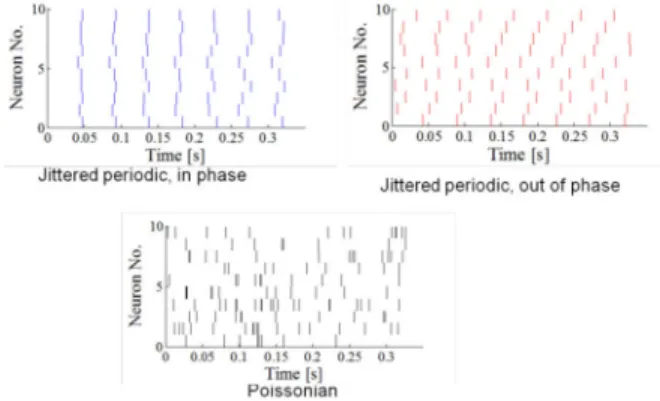
C. Stimulus encoding
Another remarkable point is the insensitivity to stimulus encoding scheme. Different schemes are possible to encode the stimulus into spikes as illustrated in Fig. 5. In the first two schemes, the input neurons spike periodically, the firing rate being proportional to the input quantity. The input neurons can spike either in phase or out of phase. This is a natural scheme based on how spiking retinas currently work [30]. In the last possibility, input neurons spike in a Poissonian way, the time constant being inversely proportional to the input. All three coding styles lead to a
TABLEI
RECOGNITION RATE ON THE MNIST TESTING SET WITH DIFFERENT KINDS OF NANODEVICE (SYNAPTIC) VARIABILITY.ALL THE SIMULATIONS WERE REPEATED 5 TIMES, THE RECOGNITION RATE GIVEN
IS AVERAGED ON THE 5 RUNS.ALL THE SIMULATIONS HAVE HOMEOSTASIS.THE DEGREE OF VARIABILITY (10%,25%,50%,100%)
IS DEFINED AS STANDARD VARIATION OF THE MEAN VALUE.
Dispersion on the parameter 10% 25% 50% 100% Initial weights 81.3% 82.0% 80.8% 81.3% Learning steps α+, α -81.8% 81.4% 79.0% 74.0% Learning steps α+,
α-, min. and max. weights wmin, wmax
81.9% 80.6% 77.2% 67.8%
TABLEII
IMPACT OF THE NEURONS’ THRESHOLD VARIABILITY, WITH AND WITHOUT HOMEOSTASIS ON THE RECOGNITION RATE.ALL THE SIMULATIONS WERE REPEATED 5 TIMES.THE DEGREE OF VARIABILITY
(10%,25%,50%) IS DEFINED AS STANDARD VARIATION OF THE MEAN VALUE.
Variability on the
neurons’ threshold Homeostasis homeostasis No No variability 81.3% 73.4%
10% 81.9% 60.2%
25% 81.2% 27.5%
performance between 81% and 82%, which again shows the robustness of the approach. This kind of robustness to spike jitter is consistent with computational neuroscience works on STDP [24].
IV. OVERALL NETWORK A. Supervised learning scheme
The second layer of the proposed architecture is a simple classical supervised classifier. It is used to label outputs of the first unsupervised layer.
For this second layer, we propose a new scheme. It is similar to the unsupervised scheme presented in the previous sections with the difference that no voltage is applied on the nanodevices when an output neuron spikes. Instead, after a pattern has been applied for a given time, input and output neurons apply a programming pulse on the nanodevices as illustrated on Fig. 6.
The input neurons apply a pulse only if they spiked during the period. Depending if the output neuron reacted as was expected, it will program the nanodevices connected to input neurons that spiked one way or another. The pulse from the input neurons (PRE) indeed contains a positive and a negative part so that by conjunction with the pulse applied to the output neuron (POST) it may program the nanodevice
one way or another.
If the output neuron was expected to spike (it corresponds to the digit actually presented), the connections to the input neurons that spiked should be strengthened. The output neuron applies a negative spike that will strengthen the positive part of pre-synaptic pulses, and increase the weights of nanodevices that present such pulses. If the output neuron was not expected to spike, inversely it should apply a positive pulse to weaken the synapses connected to input neurons that spiked. If the output neuron actually spiked (i.e. made a mistake) a significant pulse is applied to significantly reduce the weights. If it did not spike (and thus was right) – which is the most typical situation – the pulse is smaller in order to only weakly weaken the weights (and not cause the weights to decrease too rapidly).
B. Two layer scheme
The role of the supervised layer is to label neurons trained by the unsupervised first layer of section III. As illustrated on Fig. 7, this works well and in that case the insensitivity to variations is kept because labeling is not a difficult problem. Even with variations of α+, α− ,wmin, wmax of 50% the
supervised layer performance is matching perfectly the unsupervised layer.
The supervision does not improve performance, but provides a practical approach for the labeling operation. This opens up many opportunities. One promising way could be to pretrain the unlabeled layer on natural data, and then to perform a “labeling” on a small training set. This could be a useful way to process all kinds of natural data.
V. CONCLUSION
In this paper we have shown how by using a simple custom STDP scheme, memristors associated with CMOS neuromorphic circuits could perform unsupervised learning in a way that is extremely robust to variability. Non-supervision is the foundation for this tolerance and will provide extreme adaptability to the system. Homeostasis was
60 65 70 75 80 85 2 104 6 104 1 105 1.4 105 1.8 105
First (unsupervised) layer
Second (labeling) layer
Recogni
tion rat
e (%)
Iteration number
Fig. 7. Two layer learning. Learning rate of the second (labeling) layer trained by variability compatible supervision (red) compared with learning of the first layer (black), as computed in the previous section. Variability of 25% on all parameters. (initial weights, α+,
α− ,w , min w ) max
Fig. 6. Pulses for supervised learning (voltage pulses as a function of time).
Fig. 5. Illustration of the three stimulus coding schemes. Stimulus spikes timing for ten input neurons with the same pixel value in the three schemes. All three lead to a recognition rate between 81% and 82%, without any parameter needing to be adjusted.
also introduced as an essential component to retain insensitivity to CMOS variability. In the last section a scheme to use memristors for supervised learning was also introduced in a second layer. When used for labeling results of the first unsupervised layer, it retains excellent variability robustness, and provides a scheme for complete learning of real case data.
This design approach could be the groundwork for future circuits that will process natural data in a compact and low power way. Thanks to their unsupervised learning capabilities, such circuits will be able to adapt to various environments. Future work should focus on the experimental demonstration of these concepts, and to demonstrate its scaling to more complex multi-layer networks, and to other kinds of sensory stimuli.
ACKNOWLEDGMENT
The authors would like to thank S. J. Thorpe, W. Zhao, J.O. Klein, J. Saint-Martin, P. Dollfus, D. Deleruyelle and B. De Salvo for fruitful discussions and collaboration.
REFERENCES
[1] D.B. Strukov, G.S. Snider, D.R. Stewart, and R.S. Williams, “The missing memristor found,” Nature, vol. 453, May. 2008, pp. 80-83. [2] E. Marder and J.-M. Goaillard, “Variability, compensation and
homeostasis in neuron and network function,” Nat. Rev. Neurosci., vol. 7, Jul. 2006, pp. 563-574.
[3] G. Snider, “Instar and outstar learning with memristive nanodevices,” Nanotechnol., vol. 22, 2011, p. 015201.
[4] S.H. Jo, T. Chang, I. Ebong, B.B. Bhadviya, P. Mazumder, and W. Lu, “Nanoscale Memristor Device as Synapse in Neuromorphic Systems,” Nano Lett., vol. 10, Apr. 2010, pp. 1297-1301.
[5] G.S. Snider, “Self-organized computation with unreliable, memristive nanodevices,” Nanotechnol., vol. 18, 2007, p. 365202. [6] M. Versace and B. Chandler, “The brain of a new machine,” IEEE
Spectrum, vol. 47, 2010, pp. 30-37.
[7] J.H. Lee and K.K. Likharev, “Defect-tolerant nanoelectronic pattern classifiers,” Int. J. Circuit Theory Appl., vol. 35, 2007, pp. 239-264.
[8] G.S. Snider, “Spike-timing-dependent learning in memristive nanodevices,” Prof. of IEEE International Symposium on
Nanoscale Architectures 2008 (NANOARCH), 2008, pp. 85-92.
[9] J.A. Pérez-Carrasco, C. Zamarreño-Ramos, T. Serrano-Gotarredona, and B. Linares-Barranco, “On neuromorphic spiking architectures for asynchronous STDP memristive systems,” Proc. of
2010 IEEE Int. Symp. Circuits Systems (ISCAS), 2010, pp.
1659-1662.
[10] G. Snider, R. Amerson, D. Carter, H. Abdalla, M.S. Qureshi, J. Léveillé, M. Versace, H. Ames, S. Patrick, B. Chandler, A. Gorchetchnikov, and E. Mingolla, “From Synapses to Circuitry: Using Memristive Memory to Explore the Electronic Brain,”
Computer, vol. 44, 2011, pp. 21-28.
[11] Y. Lecun, L. Bottou, Y. Bengio, and P. Haffner, “Gradient-based learning applied to document recognition,” Proc. IEEE, vol. 86, 1998, pp. 2278-2324.
[12] G.W. Burr, B.N. Kurdi, J.C. Scott, C.H. Lam, K. Gopalakrishnan, and R.S. Shenoy, “Overview of candidate device technologies for storage-class memory,” IBM J. Res. Dev., 2008.
[13] F. Alibart, S. Pleutin, D. Guérin, C. Novembre, S. Lenfant, K. Lmimouni, C. Gamrat, and D. Vuillaume, “An Organic Nanoparticle Transistor Behaving as a Biological Spiking Synapse,” Adv. Funct. Mater., vol. 20, 2010, pp. 330-337.
[14] G. Agnus, W. Zhao, V. Derycke, A. Filoramo, Y. Lhuillier, S. Lenfant, D. Vuillaume, C. Gamrat, and J.-P. Bourgoin,
“Two-Terminal Carbon Nanotube Programmable Devices for Adaptive Architectures,” Adv. Mater., vol. 22, 2010, pp. 702-706.
[15] A. Afifi, A. Ayatollahi, and F. Raissi, “Implementation of biologically plausible spiking neural network models on the memristor crossbar-based CMOS/nano circuits,” European Conf.
on Circuit Theory and Design (ECCTD), 2009, pp. 563-566.
[16] H. Markram, J. Lubke, M. Frotscher, and B. Sakmann, “Regulation of Synaptic Efficacy by Coincidence of Postsynaptic APs and EPSPs,” Science, vol. 275, Jan. 1997, pp. 213-215.
[17] G.-Q. Bi and M.-M. Poo, “Synaptic modification by correlated activity: Hebb’s Postulate Revisited,” Annu. Rev. Neurosci., vol. 24, 2001, pp. 139-166.
[18] Y. Dan and M.-ming Poo, “Spike Timing-Dependent Plasticity of Neural Circuits,” Neuron, vol. 44, 2004, pp. 23-30.
[19] A. Gorchetchnikov, M. Versace, and M. Hasselmo, “A model of STDP based on spatially and temporally local information: Derivation and combination with gated decay,” Neural Networks, vol. 18, Jul. 2005, pp. 458-466.
[20] S.H. Jo and W. Lu, “CMOS Compatible Nanoscale Nonvolatile Resistance Switching Memory,” Nano Lett., vol. 8, pp. 392-397. [21] J. Borghetti, G.S. Snider, P.J. Kuekes, J.J. Yang, D.R. Stewart, and
R.S. Williams, “`Memristive’ switches enable `stateful’ logic operations via material implication,” Nature, vol. 464, Apr. 2010, pp. 873-876.
[22] J.R. Heath, P.J. Kuekes, G.S. Snider, and R.S. Williams, “A defect-tolerant computer architecture: Opportunities for nanotechnology,”
Science, vol. 280, 1998, p. 1716--1721.
[23] A. DeHon, “Array-based architecture for FET-based, nanoscale electronics,” IEEE Trans. Nanotechnol., vol. 2, 2003, pp. 23-32. [24] R. Guyonneau, R. VanRullen, and S.J. Thorpe, “Neurons Tune to
the Earliest Spikes Through STDP,” Neural Computation, vol. 17, Apr. 2005, pp. 859-879.
[25] T. Masquelier and S.J. Thorpe, “Unsupervised Learning of Visual Features through Spike Timing Dependent Plasticity,” PLoS
Comput Biol, vol. 3, Feb. 2007, p. e31.
[26] J.M. Brader, W. Senn, and S. Fusi, “Learning Real-World Stimuli in a Neural Network with Spike-Driven Synaptic Dynamics,”
Neural Computation, vol. 19, Nov. 2007, pp. 2881-2912.
[27] B. Nessler, M. Pfeiffer, and W. Maass, “STDP enables spiking neurons to detect hidden causes of their inputs,” Advances in
Neural Information Processing Systems (NIPS’09), p. 1357–1365.
[28] J.V. Arthur and K. Boahen, “Learning in silicon: Timing is everything,” Advances in neural information processing systems, vol. 18, 2006, p. 281--1185.
[29] P. Livi and G. Indiveri, “A current-mode conductance-based silicon neuron for address-event neuromorphic systems,” Proc. of
2009 IEEE International Symposium on Circuits and Systems (ISCAS), 2009, pp. 2898-2901.
[30] P. Lichtsteiner, C. Posch, and T. Delbruck, “A 128× 128 120 dB 15 μs Latency Asynchronous Temporal Contrast Vision Sensor,”
IEEE Journal of Solid-State Circuits, vol. 43, 2008, pp. 566-576.
[31] V. Chan, S.-C. Liu, and A. van Schaik, “AER EAR: A Matched Silicon Cochlea Pair With Address Event Representation Interface,”
IEEE Trans. Circuits Syst. Regul. Pap., vol. 54, 2007, pp. 48-59.
[32] M.D. Pickett, D.B. Strukov, J.L. Borghetti, J.J. Yang, G.S. Snider, D.R. Stewart, and R.S. Williams, “Switching dynamics in titanium dioxide memristive devices,” J. Appl. Phys., vol. 106, 2009, p. 074508.
[33] G. Indiveri, E. Chicca, and R. Douglas, “A VLSI array of low-power spiking neurons and bistable synapses with spike-timing dependent plasticity,” IEEE Transactions on Neural Networks, vol. 17, 2006, pp. 211-221.
[34] C. Bartolozzi, O. Nikolayeva, and G. Indiveri, “Implementing homeostatic plasticity in VLSI networks of spiking neurons,” 15th
IEEE International Conference on Electronics, Circuits and Systems (ICECS 2008), 2008, pp. 682-685.
[35] D.C. Ciresan, U. Meier, L.M. Gambardella, and J. Schmidhuber, “Deep Big Simple Neural Nets Excel on Handwritten Digit Recognition,” CoRR abs/1003.0358, Mar. 2010.