HAL Id: tel-00999475
https://tel.archives-ouvertes.fr/tel-00999475
Submitted on 3 Jun 2014HAL is a multi-disciplinary open access archive for the deposit and dissemination of sci-entific research documents, whether they are pub-lished or not. The documents may come from teaching and research institutions in France or abroad, or from public or private research centers.
L’archive ouverte pluridisciplinaire HAL, est destinée au dépôt et à la diffusion de documents scientifiques de niveau recherche, publiés ou non, émanant des établissements d’enseignement et de recherche français ou étrangers, des laboratoires publics ou privés.
drives
Hamid Khan
To cite this version:
Hamid Khan. Optimised space vector modulation for variable speed drives. Other. Université Blaise Pascal - Clermont-Ferrand II, 2012. English. �NNT : 2012CLF22288�. �tel-00999475�
N° d’ordre : D. U : 2288
E D S P I C : 582
U
NIVERSITE
B
LAISE
P
ASCAL
-
C
LERMONT
II
E
COLE
D
OCTORALE
S
CIENCES
P
OUR L
’I
NGENIEUR DE
C
LERMONT
-F
ERRAND
T h è s e
Présentée par
HAMID
HAMID
HAMID
HAMID KHAN
KHAN
KHAN
KHAN
pour obtenir le grade de
D
D
D
D
O C T E U R D
O C T E U R D
O C T E U R D
O C T E U R D
’’’’
U
U
U
U
N I V E R S I T É
N I V E R S I T É
N I V E R S I T É
N I V E R S I T É
SPECIALITE :
ÉLECTRONIQUE
DE
PUISSANCE
Optimised Space Vector Modulation for Variable Speed Drives
Soutenue publiquement le 6 Novembre 2012 devant le jury :
Pr. Bernard DAVAT
Président
Pr. Patrick Chi Kwong LUK
Rapporteur
Pr. Guy FRIEDRICH
Rapporteur
Dr. François BADIN
Examinateur
Pr. Khalil EL KHAMLICHI DRISSI
Directeur de thèse
Dr. El Hadj MILIANI
Encadrant industriel
Résumé
Le travail effectué au cours de cette thèse consiste à étudier et développer des techniques innovantes de modulation de largueurs d'impulsions (MLI) qui visent à optimiser les chaînes de traction électriques embarquées dans des véhicules hybrides ou électriques. La MLI joue un rôle stratégique au cœur des variateurs de vitesse, elle influe sur le comportement général de la chaîne de traction et sur sa performance. La MLI présente des degrés de liberté qui peuvent contribuer avantageusement à redimensionner les composants du variateur tels que le circuit de refroidissement, le filtre EMI et le condensateur du bus continu.
Les véhicules hybrides constituent une étape naturelle dans la transition énergétique entre les véhicules thermiques et les véhicules électriques.
Notre étude contribue à l'optimisation des variateurs de vitesse en général et ceux au cœur des véhicules hybrides ou électriques en particulier. Notre apport consiste à proposer une MLI performante afin de rendre le variateur plus léger et plus compacte tout en garantissant les fonctionnalités traditionnelles. La compétitivité de ces variateurs et par conséquent des véhicules hybrides ou électriques devient alors accessible.
Les véhicules hybrides ou électriques utilisent généralement une machine de
traction à courant alternatif en raison de nombreux avantages que celle ci présente par rapport à une machine à courant continu. La source d’alimentation au bord d'un véhicule est une batterie, il est donc nécessaire d'utiliser un onduleur pour transformer la tension continue en tension alternative à amplitude et fréquence variables. Le contrôle de cet onduleur est réalisé par des techniques de modulation de largeurs d'impulsions (MLI) ce qui permet ainsi de réguler le couple de la machine. Les techniques MLI produisent une composante basse fréquence, le fondamental qui est le signal désiré et des composantes hautes fréquences appelées harmoniques de commutation qui sont indésirables.
Dans les véhicules modernes, il y a de plus en plus de charges mécaniques pilotées par des machines électriques et des systèmes électroniques. Il est impératif d'éliminer le risque d'interférences électromagnétiques entre ces différents systèmes pour éviter le dysfonctionnement ou la défaillance. Il faut donc filtrer ces harmoniques indésirables pour qu'elles ne perturbent pas les calculateurs et autres circuits électroniques de faibles niveaux de tensions. Il existe des techniques de modulation aléatoire (RPWM) qui permettent d'étaler les harmoniques à la fréquence de commutation et ses multiples. Dans cette étude, notre choix s’est porté sur la technique de modulation vectorielle aléatoire (RSVM) qui présente plusieurs avantages par rapport à la MLI intersective.
machine, ces derniers pouvant être destructifs. Nous avons pu développer une technique MLI vectorielle basée sur un choix judicieux des vecteurs nuls pour réduire cette tension de mode commun.
La chaleur produite par les pertes dans les convertisseurs à commutation dure lors de l'ouverture et de la fermeture des interrupteurs doit être évacuée rapidement, ce qui réduit le stress thermique, évite la défaillance et augmente la durée de vie des interrupteurs. Une technique utilisée pour réduire ces pertes par commutation est la modulation discontinue (DPWM); une amélioration est apportée à cette technique dans ce travail. Cette amélioration est présentée sous forme d'une technique discontinue évolutive (EDSVM) qui s'adapte au régime du moteur pour minimiser les pertes. Grâce à cette technique une meilleure distribution du stress thermique sur les différents bras de l'onduleur est rendue possible et permet ainsi d'augmenter la durée de vie de l'onduleur.
Une autre variante de modulation est abordée dans ce travail; cette technique utilise des vecteurs non adjacent et un placement dynamique des pulses permettant ainsi de réduire le stress électrique sur le condensateur du bus continu et de réduire le nombre de capteurs de courants requis pour la régulation du couple de la machine.
Les effets indésirables de la MLI cités ci-dessus ont été abordés séparément et des techniques de modulation dédiées ont été développées telles que : la modulation aléatoire, la modulation discontinue et la modulation discontinue évolutive. Ces techniques permettent de réduire le filtrage passif souvent encombrant et d'utiliser des condensateurs du bus continu moins volumineux. Elles permettent également de réduire les interférences électromagnétiques (EMI) et l'effort de refroidissement.
Un banc de test complet associant l'électronique de puissance à un système de contrôle performant à base de DSP a été réalisé. Toutes les validations expérimentales sont précédées par une étude théorique et validées par simulation.
Mots clés: Electric drives, Interférence Electromagnétique, Véhicules Hybride-Electrique, Pertes par Commutation, Modulation par largeur d’impulsion, MLI Discontinue,
Abstract
The dissertation documents research work carried out on Pulse Width Modulation (PWM) strategies for hard switched Voltage Source Inverters (VSI) for variable speed electric drives. This research is aimed at Hybrid Electric Vehicles (HEV). PWM is at the heart of all variable speed electric drives; they have a huge influence on the overall performance of the system and may also help eventually give us an extra degree of freedom in the possibility to rethink the inverter design including the re-dimensioning of the inverter components.
HEVs tend to cost more than conventional internal combustion engine (ICE) vehicles as they have to incorporate two traction systems, which is the major discouraging factor for consumers and in turn for manufacturers. The two traction system increases the maintenance cost of the car as well. In addition the electric drives not only cost extra money but space too, which is already scarce with an ICE under the hood. An all-electric car is not yet a viable idea as the batteries have very low energy density compared with petrol or diesel and take considerable time to charge. One solution could be to use bigger battery packs but these add substantially to the price and weight of the vehicle and are not economically viable. To avoid raising the cost of such vehicles to unreasonably high amounts, autonomy has to be compromised. However hybrid vehicles are an important step forward in the transition toward all-electric cars while research on better batteries evolves. The objective of this research is to make electric drives suitable for HEVs i.e. lighter, more compact and more efficient -- requiring less maintenance and eventually at lower cost so that the advantages, such as low emissions and better fuel efficiency, would out-weigh a little extra cost for these cars.
The electrical energy source in a vehicle is a battery, a DC Voltage source, and the traction motor is generally an AC motor owing to the various advantages it offers over a DC motor. Hence the need for a VSI, which is used to transform the DC voltage into AC voltage of desired amplitude and frequency. Pulse width modulation techniques are used to control VSI to ensure that the required/calculated voltage is fed to the machine, to produce the desired torque/speed. PWM techniques are essentially open loop systems where no feedback is used and the instantaneous values differ from the required voltage, however the same average values are obtained.
Pulse width modulated techniques produce a low frequency signal (desired average value of the switched voltage) also called the fundamental component, along with unwanted high frequency harmonics linked to the carrier signal frequency or the PWM period. In modern cars we see more and more mechanical loads driven by electricity
harmonics have to be filtered so that they do not affect the electronic control unit or other susceptible components placed in the vicinity. Randomised modulation techniques (RPWM) are used to dither these harmonics at the switching frequency and its multiple. In this thesis a random modulator based on space vector modulation is presented which has additional advantages of SVM.
Another EMI problem linked to PWM techniques is that they produce common mode voltages in the load. For electric machines, common mode voltage produces shaft voltage which in turn provokes dielectric stress on the motor bearings, its lubricant and hence the possibility of generating bearing currents in the machine that can be fatal for the machine. To reduce the common mode voltage a space vector modulation strategy is developed based on intelligent placement of zero vectors.
For hard switched converters, commutations or the switching of the power switches produce losses that heat up the switches and have to be evacuated rapidly as thermal stress reduces the component life and makes it prone to failure. The higher the switching losses the higher the thermal stress that the switch undergoes. The heat sink dimensions are proportional to the energy lost in the form of heat to be dissipated. So higher switching losses result in a bigger heat sink. Discontinuous modulators (DPWM) are used to reduce the switching losses. Here we have developed an improved discontinuous modulator which can adapt itself to the changing machine speed and load to minimise the switching losses. It also offers the possibility to regulate the thermal stress between the inverter legs to increase the inverter life.
A PWM technique to reduce the electric stress on the DC-Link capacitors and reduce the number of current sensors required for torque regulation is presented as well. This technique makes use of non-adjacent active vectors and dynamic pulse placement.
Each of the aforementioned side effects and its alleviation is dealt with separately and dedicated modulation strategies namely Randomized, Discontinuous Space Vector Modulation and Optimised PWM in terms of reduced ripple content of the inverter input current are developed to achieve it. These techniques will eventually result in inverters with a smaller EMI filter, a smaller heat sink, smaller DC-link capacitor i.e. a compact and cheaper inverter.
A befitting test bench is realised to calculate the real gains and check the practical feasibility of these techniques in terms of execution on embedded processor. All experimental work is systematically preceded by theoretical study where analytical expressions are developed to prove the claims made and validation by simulation tools. Keywords: Electric drives, Electromagnetic Interference, Hybrid Electric Vehicles, Commutation Losses, Pulse Width Modulation, Discontinuous-PWM, Random PWM, Space Vector Modulation.
Acknowledgment
I would like to thank my two institutions, LAboratoire des Sciences et Matériaux pour l'Électronique et d'Automatique, LASMEA a Blaise Pascal university laboratory and the department of electronic systems and real time at IFP Energies Nouvelles, a renowned research firm for providing me with such an excellent research opportunity to complete my industrial PhD. This research conducted in collaboration between a university and a public sector research centre provided me with a unique and technically stimulating environment, with both an academic and industrial insights. I'd like to thank my university supervisor Mr. Khalil El Khamlichi Drissi and my industrial advisor Mr. El-Hadj Miliani for sharing their vast knowledge and their valuable experience with me. I would also like to thank my former supervisor Mr. Youssef Touzani who now works for Thales Avionics, for his encouragement and support as I adjusted to life and work in France.
I'd also like to thank the head of the department Mr. Mohammed Abdellahi Ould and the director Mr. Van Bui Tran for their belief in my capacities and the financial support they provided which enabled me to present my work in international conferences. My lab-mates and my office colleagues have been a source of encouragement, entertainment and camaraderie without which it would have been difficult going.
Finally, I cannot express my gratitude to my family and friends, who never ceased to surprise and overwhelm me with their support and faith in my success as I undertook this endeavour.
RÉSUMÉ ...3
ABSTRACT ...5
ACKNOWLEDGMENT ...7
CONTENTS ...8
LIST OF FIGURES ...10
LIST OF TABLES...13
LIST OF ABBREVIATIONS ...14
INTRODUCTION ...15
I.
PRELIMINARIES ...22
I.1. INTRODUCTION...22I.2. LITERATURE REVIEW ...23
I.2.1. Fundamentals of PWM ... 24
I.2.2. Classical Sinusoidal PWM ... 25
I.2.3. Hysteresis Band control... 26
I.2.4. Zero Sequence voltage injection ... 26
I.2.4.1. Third Harmonic Injection PWM... 28
I.2.4.2. Discontinuous PWM... 30
I.2.4.2.1. DPWM1 ... 31
I.2.4.2.2. DPWMMIN & DPMWMMAX ... 31
I.2.4.2.3. DPWM3 ... 32
I.2.5. Space Vector Modulation... 32
I.2.5.1. Sector and time calculation ... 35
I.2.5.2. Space Vector PWM... 38
I.2.6. Random PWM... 41
I.2.6.1. Random Carrier Frequency-PWM... 42
I.2.6.2. Random Pulse Position PWM ... 43
I.2.6.3. Dual Randomization... 44
I.2.7. Practical aspects of PWM... 44
I.2.7.1. Dead time... 44
I.2.7.2. Switching losses... 46
I.2.7.3. Leakage Currents... 46
I.3. ELECTROMAGNETIC INTERFERENCE...50
I.3.1. Introduction ... 50
I.3.2. EMI Standards and measurements ... 51
I.3.3. EMI Filters... 52
I.4. ANALYTICAL ANALYSIS OFPWMSCHEMES...52
I.4.1. Frequency domain analysis ... 53
I.4.1.1. Power Spectrum Density... 55
I.4.2. Waveform quality ... 55
I.4.2.1. Harmonic Voltage Distortion ... 55
I.4.2.3. Subcarrier harmonic analysis... 62
I.5. SUMMARY...66
II.
DEVELOPMENT OF PWM SCHEMES ...68
II.1. INTRODUCTION...68
II.2. DISCONTINUOUSSPACEVECTORMODULATION...68
II.2.1. Zero Vector Placement... 69
II.2.2. Evolutive Discontinuous SVM ... 70
II.2.2.1. Clamping Study... 70
II.2.2.2. Switching loss reduction ... 72
II.2.2.3. Unbalanced load condition... 76
II.2.2.4. Waveform quality ... 77
II.2.2.5. Simulations ... 79
II.2.3. Summary ... 82
II.3. RANDOMISEDSPACEVECTORMODULATION...82
II.3.1. Randomisation parameters ... 82
II.3.1.1. Sequence of vector application ... 83
II.3.1.2. Choice of active vectors ... 84
II.3.1.3. Zero vector distribution ... 86
II.3.1.4. Counter profile ... 88
II.3.2. Random number generation... 90
II.3.3. Random Space Vector Modulation... 91
II.3.3.1. Pulse Generation ... 92
II.3.3.2. Acquisition and control sequence ... 93
II.3.4. Random discontinuous modulation ... 94
II.3.5. Simulation... 95
II.3.5.1. Open loop ... 95
II.3.5.2. close loop... 96
II.3.6. Summary ... 98
II.4. PWM OPTIMIZED EMBEDDED ELECTRIC DRIVES...98
II.4.1. Introduction... 98
II.4.2. Phase current reconstruction ... 98
II.4.2.1. Limitations and Boundary conditions ... 100
II.4.2.2. State of the art ... 101
II.4.2.2.1. Reconstruction error ... 102
II.4.2.2.2. Fault Detection ... 103
II.4.2.3. Proposed solution ... 106
II.4.2.4. Simulation ... 108
II.4.2.5. Summary... 109
II.4.3. DC link capacitor reduction ... 110
II.4.3.1. Ripple component of the inverter input current ... 110
II.4.3.1.1. Reduction of input RMS ripple current ... 112
II.4.3.2. Ripple component of the inverter input Voltage ... 117
II.4.3.3. Simulation ... 120
II.4.3.4. Summary... 121
III.
EXPERIMENTAL VALIDATION ...123
III.1. INTRODUCTION...123
III.2. TEST BENCH...124
III.2.1. Power Unit ... 124
III.2.1.1. Power Converter -- VSI ... 124
III.2.1.2. DC source ... 126
III.2.1.3. Electric machine... 126
III.2.2. Control unit ... 127
III.2.3. Power and control Interface ... 129
III.2.3.1. Analog signal interfacing ... 131
III.2.3.2. Digital signal interfacing ... 132
III.3. TEST BENCH VALIDATION...133
III.3.1. ADC Modules and sensors... 133
III.3.2. Incremental encoder... 134
III.3.3. PWM Module ... 135
III.5.1.1.1. Sinusoidal Pulse Width Modulator ... 139
III.5.1.1.2. Space Vector Modulator ... 140
III.5.1.2. Discontinuous Modulator... 142
III.5.1.2.1. DPWM1 ... 142
III.5.1.2.2. DPWMMIN & DPWMMAX ... 144
III.5.1.3. Random modulator... 146
III.5.2. Dynamic Load... 148
III.5.2.1. Continuous Modulator ... 148
III.5.2.1.1. Sinusoidal Pulse Width Modulator ... 148
III.5.2.1.2. Space Vector Modulator ... 150
III.5.2.2. Discontinuous modulator... 152
III.5.2.2.1. DPWMMIN & DPWMMAX ... 152
III.5.2.2.2. EDSVM... 154
III.5.2.3. Randomised modulator ... 155
III.5.2.4. Random discontinuous modulator... 157
III.6. SUMMARY...159
IV.
CONCLUSION & FUTURE WORK...161
IV.1. CONCLUSION...161
IV.2. SUGGESTIONS FOR FUTURE WORK...163
REFERENCE...164
List of Figures
FIGURE1. WORLDCO2EMISSIONS BY SECTOR IN2009 [3] ... 16FIGURE2. PARALLELHEV DRIVETRAIN... 17
FIGUREI-1: SCHEMATIC DIAGRAM OF ANELECTRICDRIVE... 22
FIGUREI-2: HALFBRIDGE... 24
FIGUREI-3: (A), (B): NATURALLY SAMPLED, (C), (D)REGULARLY SAMPLED... 24
FIGUREI-4: ASYMMETRICALLY SAMPLED... 24
FIGUREI-5: HYSTERESISBAND... 26
FIGUREI-6: INVERTER FED FLOATING NEUTRAL 3-PHASE LOAD... 27
FIGUREI-7: GENERALIZED MODULATOR: ZSSINJECTION... 27
FIGUREI-8: FLOATING NEUTRAL... 28
FIGUREI-9: 1/4THTHIPWM ... 28
FIGUREI-10: DPWM1,MI=0.68 ... 31
FIGUREI-11: DPWM1,MI=0.907 ... 31
FIGUREI-12: DPWMMAX ... 31
FIGUREI-13: DPWMMIN ... 31
FIGUREI-14: DPWM3,MI=0.68 ... 32
FIGUREI-15: DPWM3,MI=0.907 ... 32
FIGUREI-16: VOLTAGESPACEVECTORS... 33
FIGUREI-17: SVM;MODULATION FUNCTION AND CORRESPONDING SECTORS... 35
FIGUREI-18: SVM SECTOR IDENTIFICATION... 36
FIGUREI-19:TIME CALCULATION SECTOR1 ... 37
FIGUREI-20: SVPWM... 39
FIGUREI-21: FREQUENCYSPECTRUM- PHASEVOLTAGEVA0... 39
FIGUREI-22:INCREASED LINEARITY OFMODULATIONINDEX... 40
FIGUREI-23: AMPLITUDES OF DIFFERENT MODULATION SCHEMES IN ΑΒ-PLANE... 40
FIGUREI-25:RCFM ... 42
FIGUREI-26:FREQUENCYSPECTRUMPWM-RPWM... 43
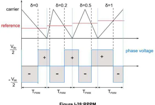
FIGUREI-27: PULSE POSITIONING... 43
FIGUREI-28:RPPM ... 44
FIGUREI-29: HALF BRIDGE... 45
FIGUREI-30: DEAD TIME... 45
FIGUREI-31: DEAD TIME; VOLTAGE DISTORTION... 46
FIGUREI-32: HARDSWITCHING... 46
FIGUREI-33: HIGH FREQUENCY MODEL OF AN ELECTRIC MOTOR... 47
FIGUREI-34:LEAKAGE CURRENT(TOP), IAANDVA0... 47
FIGUREI-35: HIGH FREQUENCY EQUIVALENT MODEL... 48
FIGUREI-36: INVERTER FEEDING TOPOLOGIES... 49
FIGUREI-37: EMIPROPAGATION... 50
FIGUREI-38: MODES OF COUPLING... 51
FIGUREI-39: CONDUCTED NOISE FILTER... 52
FIGUREI-40: FREQUENCYSPECTRUM: PWM... 54
FIGUREI-41: CARRIERHARMONICAMPLITUDES... 54
FIGUREI-42: SIDEBANDHARMONICAMPLITUDES... 54
FIGUREI-43: HARMONIC CURRENT... 58
FIGUREI-44: HDF ... 61
FIGUREI-45: HDF;SAME EFFECTIVE FREQUENCY... 62
FIGUREI-46:SPACE VECTOR,ARBITRARY REFERENCEV* ... 62
FIGUREI-47: HARMONIC VOLTAGE VECTORS... 63
FIGUREI-48: SVMSWITCHING SEQUENCE... 63
FIGUREI-49: SVM, HARMONIC FLUX TRAJECTORIES... 64
FIGUREI-50: SVM, HARMONIC FLUX... 65
FIGUREI-51: VECTOR APPLICATIONSAWTOOTH CARRIER... 65
FIGUREI-52: ΛH;TRIANGULAR AND SAWTOOTH CARRIER... 65
FIGUREI-53: VECTOR APPLICATIONDPWM... 66
FIGUREI-54: ΛHDPWMTRIANGULAR CARRIER... 66
FIGUREII-1: SVM, DSVMMAX, DSVMMIN... 69
FIGUREII-2: ZEROVECTORPLACEMENT... 70
FIGUREII-3: CLAMPING ZONES... 71
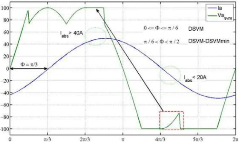
FIGUREII-4:INTELLIGENTSWITCHINGFUNCTION– Φ=30° ... 73
FIGUREII-5: INTELLIGENTSWITCHINGFUNCTION- Φ>30° ... 74
FIGUREII-6: ALGORITHMEDSVM ... 74
FIGUREII-7: SWITCHING LOSS REDUCTION Φ=0° ... 75
FIGUREII-8: SWITCHING LOSS REDUCTION Φ=30° ... 75
FIGUREII-9: SWITCHING LOSS REDUCTION Φ=90° ... 75
FIGUREII-10: SWITCHING LOSS REDUCTION-DSVM ... 76
FIGUREII-11: DSVM:UNSYMMETRICAL CLAMPING... 77
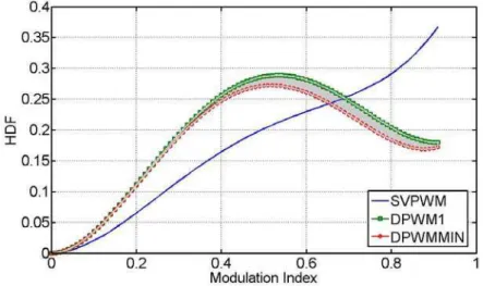
FIGUREII-12: HDF EDSVM ... 78
FIGUREII-13: HDF EDSVM;SAME EFFECTIVE FREQUENCY... 78
FIGUREII-14: HDF EDSVM;EQUAL SWITCHING LOSSES... 79
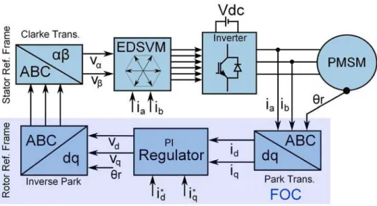
FIGUREII-15: FOCWITHDSVM ... 80
FIGUREII-16: FOC PHASOR DIAGRAM... 80
FIGUREII-17: EDSVMTORQUE RESPONSE... 81
FIGUREII-18: STATORCURRENTEVOLUTION... 81
FIGUREII-19: EDSVM- IA,DA... 82
FIGUREII-20: RANDOMVECTORSEQUENCE,TRIANGULAR CARRIER... 83
FIGUREII-21: RANDOMVECTORSEQUENCE,SAWTOOTH CARRIER... 84
FIGUREII-22: RANDOM ACTIVE VECTOR SELECTION... 84
FIGUREII-23: COMPLEMENTARYCOUNTERS... 85
FIGUREII-24: RANDOM ACTIVE VECTOR SELECTION;COMMUTATION SIGNALS... 86
FIGUREII-25: RANDOM ZERO VECTOR DISTRIBUTION... 87
FIGUREII-26:HARMONIC FLUX, ΛHFOR D0≠D7... 87
FIGUREII-27: DIGITALCOUNTER... 88
FIGUREII-28: PULSE GENERATOR... 89
FIGUREII-29: RSVMCONTINUOUS... 92
FIGUREII-34: SVM, RSVM; FREQUENCYSPECTRUMCONTRAST... 95
FIGUREII-35: RSVM STATORCURRENTEVOLUTION... 96
FIGUREII-36: FREQUENCYSPECTRUMCONTRAST(CLOSEDLOOP) ... 97
FIGUREII-37: SWITCHINGHARMONICS(RSVMANDSVM) ... 97
FIGUREII-38: THREE PHASEINVERTER AND CURRENT SENSORS... 99
FIGUREII-39: CURRENT CHANNELLING... 99
FIGUREII-40. SPACE VECTOR REPRESENTATION... 100
FIGUREII-41: MEASUREMENT VECTORS, [46]... 101
FIGUREII-42: PULSE DISPLACEMENT, [48] ... 101
FIGUREII-43:DUTY CYCLE ALTERATION, [49] ... 102
FIGUREII-44: AVERAGE CURRENT AND HARMONIC CURRENT... 102
FIGUREII-45: CURRENT RECONSTRUCTION ERROR ELIMINATION... 103
FIGUREII-46: FAULT DETECTION WITH ONE CURRENT SENSOR, [51] ... 104
FIGUREII-47: DCLINK SHORT-CIRCUIT... 104
FIGUREII-48: PHASE SHORT-CIRCUIT... 105
FIGUREII-49: GROUNDFAULT... 105
FIGUREII-50: FAULT DETECTION USING ONE CURRENT SENSOR, [50] ... 106
FIGUREII-51: TRIANGLE AND SAWTOOTH MODULATION... 107
FIGUREII-52: PHASE CURRENT DEDUCTION;HIGH MIAND SECTOR EXTREMITIES... 108
FIGUREII-53: DISCONTINUOUSPWMFOR PHASE CURRENT DEDUCTION... 108
FIGUREII-54: PHASE CURRENT IN THE ΑΒ-PLANE... 109
FIGUREII-55: CURRENT IN THEDC-LINK... 110
FIGUREII-56: TWO NON-ADJACENT VECTORS–CASE1 ... 113
FIGUREII-57: TWO NON-ADJACENT VECTORS–CASE2 ... 114
FIGUREII-58: THREE NON-ADJACENT VECTORS... 115
FIGUREII-59 THREE ADJACENT VECTORS... 115
FIGUREII-60: RMSINPUT CURRENT RIPPLE... 117
FIGUREII-61: RMSINPUT VOLTAGE RIPPLE... 119
FIGUREII-62: IDCANDIABC, SVM. E.G.-1 ... 120
FIGUREII-63:IDCANDIABC, OPT. E.G.-2 ... 120
FIGUREII-64: IDCANDIABC, SVM. E.G.-2 ... 121
FIGUREII-65: IDCANDIABC, OPT. E.G.-2 ... 121
FIGUREIII-1: TEST BENCH,SCHEMATIC DIAGRAM... 123
FIGUREIII-2: INVERTERV-ICHARACTERISTICS... 124
FIGUREIII-3: INVERTER MODULE... 125
FIGUREIII-4: IGBT SWITCHING CHARACTERISTICS... 125
FIGUREIII-5: DCSOURCE... 126
FIGUREIII-6: ELECTRICMACHINE... 126
FIGUREIII-7: F28X ARCHITECTURE... 127
FIGUREIII-8: RAPID PROTOTYPING... 128
FIGUREIII-9: SIMULATION IN THELOOP... 129
FIGUREIII-10: AUTOMATIC CODE GENERATION... 129
FIGUREIII-11: SCHEMATIC DIAGRAM OF THE INTERFACE CIRCUIT... 130
FIGUREIII-12: ANALOGSIGNALSCALING... 131
FIGUREIII-13: ANTI-ALIASING FILTER... 131
FIGUREIII-14: INTERFACE BOARD... 132
FIGUREIII-15: TEST BENCH... 133
FIGUREIII-16: ADCCALIBRATION... 134
FIGUREIII-17: CURRENT CALIBRATION... 134
FIGUREIII-18: ENCODER VERIFICATION... 135
FIGUREIII-19: PWMSIGNALS FROMDSP... 135
FIGUREIII-20: WTHD0FORSPWMFOR DIFFERENT PULSE RATIOS... 137
FIGUREIII-21: INVERTER FEEDING A STATIC LOAD... 138
FIGUREIII-22: SPWM: PHASE VOLTAGE AND CURRENT... 139
FIGUREIII-23: SPWM: HARMONIC SPECTRUM... 139
FIGUREIII-24: SPWM:FREQUENCY SPECTRUM... 140
FIGUREIII-26: SVM: HARMONIC SPECTRUM... 141
FIGUREIII-27: SVM:FREQUENCY SPECTRUM... 142
FIGUREIII-28: DPWM1: PHASE VOLTAGE AND CURRENT... 143
FIGUREIII-29: DPWM1: HARMONIC SPECTRUM... 143
FIGUREIII-30: DPWM1 SPWM:FREQUENCY SPECTRUM... 144
FIGUREIII-31: DPWMMAX: PHASE VOLTAGE AND CURRENT... 144
FIGUREIII-32: DPWMMIN: PHASE VOLTAGE AND CURRENT... 144
FIGUREIII-33: DPWMMIN: HARMONIC SPECTRUM... 145
FIGUREIII-34: DPWMMAX: HARMONIC SPECTRUM... 145
FIGUREIII-35: DPWMMIN:FREQUENCY SPECTRUM... 145
FIGUREIII-36: DPWMMAX:FREQUENCY SPECTRUM... 145
FIGUREIII-37: SVM: PHASE VOLTAGE AND CURRENT... 146
FIGUREIII-38: RSVM: PHASE VOLTAGE AND CURRENT... 146
FIGUREIII-39: RSVM: HARMONIC SPECTRUM... 147
FIGUREIII-40: DPWMMAX:FREQUENCY SPECTRUM... 147
FIGUREIII-41: SPWM: PHASE VOLTAGE AND CURRENT... 149
FIGUREIII-42: VECTOR CONTROLLEDSPWM: HARMONIC SPECTRUM... 149
FIGUREIII-43: VECTOR CONTROLLEDSPWM:FREQUENCY SPECTRUM... 150
FIGUREIII-44: VECTOR CONTROLLEDSVM: PHASE VOLTAGE AND CURRENT... 150
FIGUREIII-45: VECTOR CONTROLLEDSVM: HARMONIC SPECTRUM... 151
FIGUREIII-46: VECTOR CONTROLLEDSVM:FREQUENCY SPECTRUM... 151
FIGUREIII-47: VECTOR CONTROLLEDDSVMMAX: PHASE VOLTAGE AND CURRENT... 152
FIGUREIII-48: VECTOR CONTROLLEDDSVMMIN: PHASE VOLTAGE AND CURRENT... 152
FIGUREIII-49: VECTOR CONTROLLEDDPWMMAX: HARMONIC SPECTRUM... 153
FIGUREIII-50: VECTOR CONTROLLEDDPWMMIN: HARMONIC SPECTRUM... 153
FIGUREIII-51: VECTOR CONTROLLEDDPWMMIN:FREQUENCY SPECTRUM... 153
FIGUREIII-52: VECTOR CONTROLLEDDPWMMAX:FREQUENCY SPECTRUM... 153
FIGUREIII-53: VECTOR CONTROLLEDEDSVM: PHASE VOLTAGE AND CURRENT... 154
FIGUREIII-54: VECTOR CONTROLLEDEDSVM: HARMONIC SPECTRUM... 154
FIGUREIII-55: VECTOR CONTROLLEDEDSVM:FREQUENCY SPECTRUM... 155
FIGUREIII-56: VECTOR CONTROLLEDSVM: PHASE VOLTAGE AND CURRENT... 156
FIGUREIII-57: VECTOR CONTROLLEDRSVM: PHASE VOLTAGE AND CURRENT... 156
FIGUREIII-58: VECTOR CONTROLLEDRSVM: HARMONIC SPECTRUM... 156
FIGUREIII-59: VECTOR CONTROLLEDRSVM:FREQUENCY SPECTRUM... 157
FIGUREIII-60: VECTOR CONTROLLEDRDSVM: PHASE VOLTAGE AND CURRENT... 157
FIGUREIII-61: VECTOR CONTROLLEDRSVM: HARMONIC SPECTRUM... 158
FIGUREIII-62: VECTOR CONTROLLEDRSVM:FREQUENCY SPECTRUM... 158
List of Tables
TABLEI-1 COMPARISON OFELECTRICALMACHINES... 23TABLEI-2 VECTOR MAGNITUDES IN ΑΒ-PLANE... 34
TABLEI-3 ATTAINABLEVOLTAGE USING DIFFERENT TECHNIQUES... 41
TABLEI-4: VCMFOR A SINGLE PHASE FULL WAVE RECTIFIER... 49
TABLEII-1: PHASE CURRENT AND SPACE VECTORS... 99
TABLEIII-1: MACHINE CHARACTERISTICS... 127
TABLEIII-2: EXPERIMENTAL PERFORMANCE COMPARISON OF DIFFERENTPWMSTRATEGIES... 148
DPWM Discontinuous Pulse Width Modulation
DFT Discrete Fourier Transformation
DSP Digital Signal Processor
DSVM Discontinuous Space Vector Modulation
DTC Direct Torque Control
ECU Electronic Control Unit
EMC Electromagnetic Compatibility
EMF Electromotive Force
EMI Electromagnetic Interference
FFT Fast Fourier Transformation
FOC Field Oriented Control
HEV Hybrid Electric Vehicle
ICEV Internal Combustion Engine Vehicle
IGBT Insulated Gate Bipolar Transistor
MOSFET Metal Oxide Field Effect Transistor
PMSM Permanent Magnet Synchronous Motor
PSD Power Spectral Density
PWM Pulse Width Modulation
RCF Random Carrier Frequency
RPP Random Pulse Position
RPWM Random Pulse Width Modulation
RSVM Random Space Vector Modulation
SVM Space Vector Modulation
THIPWM Third Harmonic Injection PWM
THD Total Harmonic Distortion
VSI Voltage Source Inverter
List of Notations
ga Upper switch Gating signal for phase 'a'
<Va>T Mean phase voltage over a modulation period
Ca Clamping duration phase 'a'
CNK Fourier coefficients
Cws Parasitic capacitance between the stator windings and stator frame
E Back EMF of the machine
f(mi) Harmonic distortion factor
fPWM Carrier frequency
ih Harmonic current
L Inductance
mi Modulation index
Psw Switching losses
S(f) Power density spectrum
u0 Zero sequence voltage
V*a Voltage reference, phase 'a'
Va0 Phase 'a' voltage with respect to DC mid-point
Van Phase voltage with respect to the load neutral
VCM Common mode voltage
Vdc Inverter input voltage
Vi Space vectors (i=0,1,2,3,4,5,6,7)
vmax Maximum instantaneous value of a 3 phase system
Vn0 Potential difference between load neutral and the DC mid-point
Vα, Vβ Voltages in αβ-plane
αi Duty cycle of space vectors
λh Harmonic flux
Vehicles contribute enormously to atmospheric pollution, about 20%-35% of total atmospheric pollution [1]. An average European car produces about 4 tonnes of CO2every
year [2], [3]. These emissions can be classified further as exhaust emissions including dangerous gases such as carbon monoxide, oxides of nitrogen, hydrocarbons and particulates and evaporative emissions vapours of fuel which are released into the atmosphere without being burnt. Some of these gases contribute to the greenhouse effect which is a threat to the planet.
EVs or HEV can help to considerably reduce these emissions. Depending on the way the electricity is produced and on the type and extent of electrification of the vehicle (e.g. micro hybrid, mild hybrid, Plug in HEVs range extenders, pure electric etc.) the emissions can be reduced from 5% to 100%. Statistics for some HEVs are given in Table I. Toyota Prius is most sold HEV.
Figure 1. World CO2emissions by sector in 2009 [3]
Figure 1 shows the carbon dioxide emissions by sector for the year 2009. It is clear that transport represents the second largest chunk on the pie chart, however electricity and heat remain the biggest contributors of this greenhouse gas. Hence all the more reason to concentrate on Hybrids rather than on all-electrics, until we get this percentage down. However this doesn't apply to countries which do not use fossil fuel to generate electricity. The 'Other' on the chart includes commercial/public services, agriculture/forestry, fishing, energy industries other than electricity and heat generation, and other emissions not specified elsewhere.
CO2 Reduction (%)
Fuel consumption Reduction (%)
Toyota Prius 42 38
Ford Fusion Hybrid 36 31
Lincoln MKZ Hybrid 36 31
Honda Civic Hybrid 31 28
Lexus HS 250h 30 28
Mazda Tribute Hybrid 26 23
Nissan Altima Hybrid 21 19
Table I. HEV pollution reduction
ICEVs give good performance and autonomy, taking advantage of the rich petroleum fuels. The efficiency and pollution of such vehicles is a threat to the environment and limited energy reserves. Whereas battery powered EVs have high efficiency and zero emission but very low operating range per battery charge. HEVs have the advantages of an ICEV and an EV while alleviating their drawbacks [1], [6]. Since HEVs have two energy sources and converters it could considerably increase the cost and space requirements as can be seen in Figure 2. Many types of hybrid structures are possible like series, parallel, series-parallel and complex hybrid [7]. Parallel hybrid best meets the objective of increased efficiency and low emissions. There are serious drawbacks of the series hybrid drivetrain, such as the energy conversion takes place twice and the electric traction motor needs to be rated for maximum power. Whereas for a parallel drivetrain, a complex mechanical coupling design is required with the additional complexity of regulating/blending two parallel power sources [8], [1].
Figure 2. Parallel HEV Drivetrain
Regenerative braking, or energy recuperation, is the principal means through which the kinetic energy of the vehicle is returned to electric energy storage rather than burned off as heat in the brake pads. But there are practical limits to how much and how fast
result of a fine balance between electric motor energy recuperation and the vehicle’s foundation brakes. The best brake system for a hybrid is what is known as series regenerative braking system (RBS). With series RBS the electric motor extracts braking energy without application of the service brakes, then when higher braking forces are required, or if the brake pedal is depressed faster than a prescribed threshold, the service brakes are engaged so that total braking effort is delivered. Not only are such cars energy efficient they have better performance owing to very dynamic torque response, particularly under Field Oriented Control (FOC), it is quicker than ICE response. During gear-shifting the electric motor can add torque to the driveline, thus filling in for lack of engine-supplied torque and give a better driving experience. Hybrid electric power trains require a large investment in electric motor and power electronics technology. Package space is extremely restricted so that even with a ground-up design for a hybrid there is little space to put 20 to 100 kW electric machines and the power electronics to drive them. Such machines must not only have the highest power density but they must also be robust and efficient. The power electronics must be of the highest power density both gravimetrically and volumetrically [1].
Nonetheless EVs have already penetrated the off-road vehicles where the required autonomy is not the limiting factor and is known beforehand and where low acoustic noise and clean air are a priority. Such applications include airport vehicles for passenger and ground support; recreational vehicles like golf carts and for theme parks, plant operation vehicles like forklifts and loader trucks. All of this is possible because of the technological advancements in power electronics and digital signal processors. The recent developments in the field of power solid state devices or Power Electronics has changed completely the form of electric propulsion system, it has made the use of AC machines possible. Here we'll discuss electric drives with a portable energy source, the battery for automotives. A typical modern electric drive is shown in Figure I-1. The AC motor is fed by a battery via a Voltage Source Inverter (VSI), it can be seen as the interface between the DC voltage source (battery) and the AC Motor. The inverter can convert DC Voltage in a poly phase AC voltage source of variable amplitude and frequency. They are made up of power switches that can be electronically switched on and off. These electronic signals are voltage pulses for IGBTs, which have been used in this work as they meet our power and frequency requirements. An Electronic Control Unit (ECU) calculates the duty cycle of the pulses using the information fed to it by an acquisition circuit, this is known as Pulse Width Modulation.
The research revolves around the development of modulation techniques for hard switched three phase two level inverters for variable speed drives destined for HEV to alleviate the drawbacks of the hybrid drivetrains mentioned above. Random and discontinuous modulation techniques have been developed to address the issues of EMI
interference and switching losses respectively and their digital implementation has been given equal importance. Techniques to reduce DC-link capacitors are also developed.
Hard switched PWM converters have the following drawbacks:
1) Electromagnetic pollution caused by the switching harmonics and switching transients [11] may hamper the proper functioning of digital electronic circuitry used extensively in modern cars. This is normally dealt by adding bulky and voluminous L-C filters and shielding of the power converter.
2) Switching Losses [12] are not only a waste of energy but give rise to another very important concern -- evacuating this energy dissipated in the form of heat in the power switches. Thermal stress can lead to poor functioning and in extreme cases complete failure of the switch.
3) Shaft voltages may cause an electric discharge through the lubricant around the ball bearing and the stator called bearing current and destroy the motor [13].
4) Acoustic noise in power converters [14] for switching frequencies in the audible range till 22kHz can be very annoying.
To alleviate these drawbacks this work has the objective of reducing the cost and volume of the electric drivetrain by developing innovative PWM techniques to reduce the need of auxiliary components required to suppress the side effects of such systems namely EMI, DC link fluctuations and heating of the power switches and at the same time increasing the efficiency and hence an improved autonomy on battery. These auxiliaries are namely the passive filters to absorb the switching harmonics, DC stabilizing capacitors and voluminous cooling circuit.
A very important aspect of this research is the integration of EMI mitigation
techniques and meeting Electromagnetic Compatibility (EMC) standards at the
development stages of the electric drive rather than troubleshooting at the end, which is a costly and time-consuming process. The motivation behind the work is to reduce the cost to market of HEVs which is significantly higher than conventional cars. Innovative techniques based on the classical PWM techniques such as RPWM and DPWM exist to address the issue of unwanted harmonics linked to the switching frequency and the switching losses. These techniques are explained in the chapters to follow. Space Vector Modulation (SVM) is a relatively new PWM technique based on mathematical transformations and has some advantages over conventional techniques. Since more and more sophisticated techniques are used, such as FOC, DTC, the digital signal processors have become indispensible and this means SVM can be implemented at no extra cost. SVM has been taken as the basic modulation technique and its derivatives are developed to address the issues mentioned above.
In such electric drives, PWM methods influence heavily the behaviour of the drive. A meticulously programmed technique cannot only give improved performance but also reduce many of the unwanted secondary effects of modulated power supply. The work
The thesis is divided into four parts, the first part puts into perspective the need for this study and an assessment of the state of the art of the field, explaining briefly the major problems that need to be addressed. Introduction to EMI is given and then an overview of some performance indicators of Pulse Width Modulators. The second part gives details of the PWM techniques developed during this PhD. The third part gives the details of the experimental setup and the experimental validations of the techniques developed in the second part. The fourth part is the conclusion and few suggestions for future works.
PART I
I. Preliminaries
The research documented in this thesis relates to pulse-width modulation (PWM) techniques for hard-switched three phase two level power electronic inverters for variable speed drives destined for vehicle propulsion. Focus has been on two different types of modulators that introduce randomness and discontinuity to the system for reasons to be described shortly. Such modulators are generally designated as random PWM techniques in the literature to emphasize their non-deterministic properties.
I.1. Introduction
An electric drive comprises of an inverter which interfaces the energy source to the motor/generator. In the context of vehicle propulsion system the inverter helps feeding the motor as required by the driver but also recharging the batteries during deceleration and braking. The inverter is comprised of electronically controllable switches. The PWM schemes control the state of the switches whether conducting or not. The maximum DC side voltage is about 600V hence 2 level IGBT inverters are sufficient. However to improve the signal quality one can imagine the use of multilevel inverters but for automotive applications it is not practical owing to the extra cost it will add to the overall system, i.e. extra gate drivers, extra PWM peripherals, extra processing power, extra space.
Figure I-1: Schematic diagram of an Electric Drive
Permanent Magnet Synchronous Motor (PMSM) are preferred as they are superior to the DC and induction motors in servo applications due to their high power density, efficiency, moment to current ratio and their low moment of inertia [9]. Permanent Magnet Synchronous Motors (PMSM) have been unanimously declared to be the most suitable for
HEVs. Table I-1 recapitulates how different electrical machines fair on grounds mentioned above. DC IM PMSM SRM Power Density -- + ++ 0 Efficiency -- + ++ 0 Cost + + 0 +
Table I-1 Comparison of Electrical Machines
The two most pertinent control schemes for AC motors are Field Oriented Control (FOC) and Direct Torque Control (DTC). The former was chosen because DTC is a method based on hysteresis comparators which require the controller to work at a very high frequency in order to confine the error in the hysteresis band which means introducing error to the system and hence torque ripple. FOC unlike DTC is based on regulators which calculate the exact value of the phase voltage to be fed to the motor. PWM techniques are used to calculate the duty cycle of the pulse to be applied to the switch to produce the required output voltage to be applied to the motor [10]. PWM techniques are at the heart of such drives, they have a huge influence on various aspects apart from the quality of the voltage produced, like the losses and electromagnetic interference.
I.2. Literature review
Pulse Width Modulation is an interface between the control circuit and the inverter, where the modulator is given a value that is required at the converter terminal and it has to produce it for a given period and a given DC voltage. Modulation technique was developed by communication engineers to transmit a baseband signal by transforming it into a pass-band signal. The use of PWM for electric drives dates as back as the early 1960s [15].
The concept is to achieve a variable voltage from a fixed DC voltage source while regulating the duty cycle of the power converter control signal. Half bridge or a converter leg configuration is shown in Figure I-2. The control signals gaand ga' of the two switches
S1 and S2 are complementary in nature. The voltage output (Va0) for a sinusoidal reference
signal (V*a) is the modulated signal generated by comparing a high frequency carrier wave
with the reference signal, the switch changes state each intersection of the these two signals The voltage produced is known as Pulse Width Modulated Voltage. The average value of the modulated voltage over a carrier period is equal to the reference voltage for that carrier period this is also known as Volt-Sec match. For good results the carrier frequency should be at least 20 times higher than the fundamental frequency.
Figure I-2: Half Bridge
I.2.1.
Fundamentals of PWM
Different types of carrier signal and the frequency of the reference voltage updates schemes can be envisioned and some of the most common methods are discussed here. The two predominant carrier signals used are sawtooth, triangular and the reference voltage updates usually employed are naturally sampled, regularly sampled (symmetrical and asymmetrical).
Figure I-3: (a), (b): Naturally sampled, (c), (d) regularly sampled
The naturally sampled scheme is realized by an analog circuit and therefore the comparator is updated continuously and thus the most accurate. Whereas other techniques such as symmetrical, asymmetrical, multi-sampled schemes are digitally implemented using DSP/FPGA. In Figure I-3 and Figure I-4 the evolution the reference signal is highly exaggerated as the carrier is very high compared to the reference signal frequency for a carrier period the reference signal can be considered constant.
I.2.2.
Classical Sinusoidal PWM
Three half bridges in parallel form a three phase inverter. For a 3-phase system given by (1.1) the voltage reference of each leg is phase delayed by 120°.
* * *
sin ( )
sin (
2
)
3
sin (
4
)
3
a b cA
v
v
v
(1.1)The most basic and straight forward PWM strategy is the Sinusoidal PWM. This method is used specially for loads with neutral tied to the ground or the DC mid-point.
*
2
(1
) 100
2
{ , , }
PWM i dc iT
v
d
v
wherei
a b c
(1.2)Equation (1.2) gives the duty cycle in percentage of the modulation period 'TPWM' for
symmetrically sampled PWM. Since the duty cycle cannot be greater than 100, again from equation (1.3) one can deduce that the amplitude of the reference is limited to half of Vdc.
Hence the maximum value of A is Amax=Vdc/2.
Modulation Index (mi) is given by (1.3) to evaluate the extent to which the DC input
voltage is used.
fundamental PWM i
fundamental six step
V m V (1.3)
Six step refers to square wave phase voltage were for the positive half cycle the phase is clamped to the positive terminal of the DC source and for the negative half to the negative terminal hence the voltage is not modulated and produces the maximum output voltage. This definition of mi is chosen so because it makes sure that
0
m
i1
. Thefundamental component of a square wave is 2 Vdc/ π. So the modulation index for SPWM
is 4
or 0.785.Frequency domain analysis of the modulated signal helps visualizing the presence of the reference signal in the square pulse train. The switching harmonics are the by-product of the PWM, frequency domain analysis of the PWM signals are elaborated later in the thesis. These unwanted high frequency voltage causes conducted and radiated electro-magnetic emissions. Passive filters are used to send back these voltages back to the source and absorb some of these unwanted signals however to reduce the filtering effort one can use Random PWM methods explained in the next section.
I.2.3.
Hysteresis Band control
Before we go further I'd like to mention a slightly different type of controller, called the hysteresis controller or a current regulator. As the name current regulator suggest this technique directly controls the current in the inverter. What distinguishes it from the other PWM techniques is that it is technique is a closed loop technique i.e. it requires a feedback. This is the most basic current control method that doesn't require current regulators. The switches are controlled to maintain the current around the desired value defined by the hysteresis band (HB). As indicated in Figure I-5, if the actual current exceeds the HB, the upper device of the half-bridge is turned off and the lower device is turned on. As the current decays and crosses the lower band, the lower device is turned off and the upper device is turned on. If the HB is reduced, the harmonic quality of the wave will improve, but the switching frequency will increase, which will in turn cause higher switching losses.
Figure I-5: Hysteresis Band
Basically, the current loop error signal generates the PWM voltage wave through a comparator with a hysteresis band. Although the technique is simple, control is very fast, and device current is directly limited, the disadvantages are a harmonically non-optimum waveform and the phase lag is frequency dependent, increases with the increase in frequency.
I.2.4.
Zero Sequence voltage injection
If the neutral point on the poly-phase load has a floating neutral i.e. not connected to the DC side midpoint 0 or the ground, the zero sequence signals (ZSS) in the phase voltages disappear from the line voltages and thus the phase currents depend only on the potential difference between the phases and the phase to neutral voltages are perfectly sinusoidal and in turn the phase currents.
A 3-phase 3-wire system, i.e. neutral free to float with respect to the ground or the DC mid-point is shown in Figure I-6.
Figure I-6: Inverter fed floating neutral 3-Phase load
However certain rules must be followed while inserting ZSS into the reference voltages. In equation (1.4) the u0is the ZSS voltage added and u* is the original reference
voltage generally sinusoidal and u** is the final voltage seldom a sinusoid of different amplitude.
** *
0
u u u (1.4)
Figure I-7 shows a generalised modulator commonly abbreviated as GPWM.
Figure I-7: Generalized modulator: ZSS injection
Figure I-8 helps visualize the concept of floating neutral and how one can achieve higher phase voltages injecting the right zero sequence component without creating an imbalance, in the next section we'll see what ZSS should be injected if the goal is to achieve higher phase voltages. Whatever be the zero sequence voltage injected into the system it should not make the phase voltages go beyond the maximum calculated value, beyond this value it will introduce imbalance in the system. Another very important aspect about ZSS component is the possibility of adding discontinuity to the modulator.
Figure I-8: Floating neutral
From the above figure the maximum value of the phase to neutral voltage can be calculated.
max max
max max max max
max
240
0
cos 30
cos 30
cos 60
cos 60
2cos 30
3
an bn DC dc dc dc dcV
V
V
V
V
V
V
V
V
V
V
V
V
V
max3
dcV
V
(1.5)From the above derivation it is evident that there are limits to the ZSS that can be added without creating an imbalance in the poly-phase system.
I.2.4.1.
Third Harmonic Injection PWM
Third harmonic injection PWM (THIPWM) can increase the value of the fundamental component of the phase voltage, Figure I-9 shows that after the addition of the zero sequence component the region which would have been over-modulated or un-modulated is now under linear modulation region. The optimum injection value can be calculated as following: [16].
The most prominent third harmonic injection schemes are THIPWM1/4 and THIPWM1/6 where the zero sequence voltage to be injected is given by (1.6).
0 3 1 1 3 3
cos(3
)
4
6
u
A
t
A
A
A
or A
(1.6)Where A1 and A3 are the amplitudes of the fundamental and the third harmonic components respectively. Injecting ¼ of the fundamental is theoretically superior in terms of harmonic distortion [17] while injecting 1/6 increases the fundamental to the maximum possible value , this can be shown in the following manner: Let Eq.(1.7) give the resultant voltage after third-harmonic injection.
1cos 3cos 3
2 dc a V V M
M
(1.7) Dividing by 12
dcM V
we get: cos cos 3 v
Where 3 1M
M
. sin 3 sin 3 0 dv dt
(1.8)The maxima or minima of (1.7) would lie on the values of θ and
that satisfy equation (1.8) and sin3θ can be written as:2
sin 3
(4cos
1)sin
Substituting it in equation (1.8) gives
2
sin
3 (4 cos
1) sin
0
from where the value of cosθ can be calculated as:3 1
cos
12
(1.9)cos3θ can similarly be expanded to give as 2
cos 3
(4 cos
3) cos
and therefore6 1 3 1 cos 3 6 12
.Substituting these values back in (1.8) give:
max 3 1 3 1 3 3 v
(1.10)Differentiating this time with .respect to γ and equating to 0. max 2 1 1 3 1 1 1 1 3 6 1 3 1 3 dv d
1
1
0
1
(1
)
3
6
We get two values of
.1 1
&
3 6
(1.11)The first one can be neglected and clearly produces 0 when substituted in (1.10). Hence a minimum.
With the second value of
the maximum attainable fundamental component isfound. 1,max
3
dcV
A
(1.12)It should be noted that the amplitude is one-sixth of the A1,max given by equation (1.12). It is the same value that was calculated earlier in this chapter hence it confirms that injecting this ZSS the maximum possible phase voltage can be achieved.
I.2.4.2.
Discontinuous PWM
ZSS can be injected in the system not only to make better use of the DC link voltage, it can also reduce the effective switching frequency over a fundamental period avoiding commutations during a part of the fundamental period. The idea behind such techniques is clamping a phase to either side of the DC rail. To clamp phase 'i' the following condition must be met:
*
max min
i
v
v
v
(1.13)This condition basically assures that the line voltages will not be distorted and since line voltages dictate the current in the phases for loads with floating neutral. Respecting this condition one can imagine quite a few discontinuous techniques. The commonly found techniques in the literature are briefly covered here. All the figures in this section show three waveforms: the zero sequence signal in red, the initial voltage reference signal in black and the new resultant signal (blue) u**. In this method the voltage clamping is symmetrical for the positive and negative half cycles.
I.2.4.2.1.
DPWM1
DPWM1 is one of the most basic types of modulation scheme where the phase with the maximum absolute amplitude is clamped. The expression of the voltage to be injected in this case is given by (1.14).
0 ( max) max
2
dc
V
u sign v v (1.14)
Figure I-10: DPWM1, mi=0.68 Figure I-11: DPWM1, mi=0.907
Where Vmax= max(abs(Va, Vb, Vc). Figure I-10 and Figure I-11 show the DPWM1
method for two different modulation index.
I.2.4.2.2.
DPWMMIN & DPMWMMAX
Voltage clamping for these methods is done either at maximum voltage or minimum. This method unlike DPWM1 is an unsymmetrical method where clamping is done only during one of the two half cycles for 120°. The harmonic injection law for DPWMMIN is given by (1.15): 0 min 2 dc V u v (1.15)
Figure I-12: DPWMMAX Figure I-13: DPWMMIN
Similarly the zero sequence component to be inserted is given by equation (1.16). Figure I-12 and Figure I-13 show the modulation functions for DPWMMAX and DPWMMIN respectively.
0 max 2 dc V u v (1.16)
I.2.4.2.3.
DPWM3
DPWM3 has four 30° discontinuous segments as can be seen in Figure I-14 and Figure I-15, the zero sequence voltage to be injected is given by:
max min
0
(
1)
(
1)
2
dc
signV
sign
V
sign
V
u
(1.17)If |Va|<|Vb|<|Vc|, then sign=1 if Va>0 and -1 otherwise.
Figure I-14: DPWM3, mi=0.68 Figure I-15: DPWM3, mi=0.907
The reference signal with the intermediate magnitude defines the zero sequence signal. This method has low harmonic distortion characteristics [20].
0 * * *
(
)
2
,
max (
(
) ,
(
) ,
(
) )
{0, 30 , 60 }
dc max max max a b cV
u
sign v
v
where
v
v
t
v
t
v
t
(1.18)There are plenty of methods to achieve voltage clamping but they are not all discussed here as the only the concept was to be introduced and only most of common of these discontinuous modulators discussed. Such modulators are called generalized discontinuous modulator where a generic type of zero sequence can be added [19].
I.2.5.
Space Vector Modulation
Space vector modulation (SVM) is a digital modulation technique based on mathematical transformation. A three phase electrical system can be represented on the αβ-plane using the well-known Clark transform (1.20). as shown in Figure I-16. to calculate the duration of the active vectors to applied [16], the modulation period is completed by the zero vectors(V0 and V7). Figure I-16 depicts the vectors representing all possible inverter states that form the vertex of a hexagon on the αβ-plane.
Figure I-16: Voltage Space Vectors
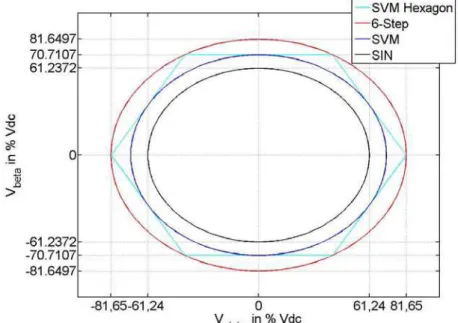
The three bit binary subscript denotes the state of upper switch of the inverter leg corresponding the three phases 'a, b and c' in the same order. '0' and '1' represent the OFF and ON state respectively. The upper and lower switch states of a leg are complimentary to avoid short circuiting the voltage source. The other vectors are to be interpreted in the same way. SVM is the generation of a voltage vector using two adjacent vectors among the six active vectors (explained later in document) and the two zero vectors.
The phase voltages 'vin' are given by (1.19).
2 1 1 1 1 2 1 3 1 1 2 1 ( ) & { , , } 2 a n a o b n b o c n c o i o dc i v v v v v v where v V g i a b c (1.19)
A 3-phase system can be projected on the αβ-plane using the following transformation. 1 1 1 2 2 2 3 3 3 0 2 2 a b c x x
x
x
x
(1.20)Applying (1.20) and (1.19) on (1.1) we get the projections in the αβ-plane as shown in the Table I-2.
ga gb gc vα vβ Vector 0 0 0 0 0 V0 0 0 1 6 dc V 2 dc V V5 0 1 0 6 dc V 2 dc V V3 0 1 1 2 6 dc V 0 V4 1 0 0 2 6 dc V 0 V1 1 0 1 6 dc V 2 dc V V6 1 1 0 6 dc V 2 dc V V2 1 1 1 0 0 V7
Table I-2 Vector magnitudes in αβ-plane
The magnitudes of all the active vectors can be given by (1.21). 2 3 {1, 2,3, 4,5,6} i dc V V wherei (1.21)
Using (1.20) a balanced three phase system expressed by (1.1) can be represented by a circle whose radius is given by A.
3 sin( ), 2 3 cos( ) 2 v A v A
(1.22) 2 23
2
v
v
A
(1.23)Let Amax be the maximum amplitude of the 3-phase Voltage that can be generated
using the space vectors shown in Figure I-16. Then the radius of such system is given by (1.24).
max max
3
2
r
A
(1.24)The circle inscribed in the hexagon represents a circle whose radius is 'rmax'. Hence
this defines the boundary limit of the attainable voltage. From the (1.24) we get (1.25).
max
2
cos
3
dc6
r
V
(1.25)Comparing (1.24) and (1.25) we get Amax as expressed by (1.26).
max
3
dc
V
A
(1.26)I.2.5.1.
Sector and time calculation
The Space vector hexagon can be divided into six parts according to the six active vectors. They are called sectors. A vector in any sector can be produced as the resultant of the two vectors defining the sector. Active vector application duration is calculated with the help of Figure I-16 in the following manner.
Figure I-17: SVM; modulation function and corresponding sectors
For a balanced three phase system the space vector modulation function and sectors in the time domain are shown in Figure I-17. Each sector is 60° long i.e. one-sixth of the fundamental period.
The αβ-plane is divided by lines;
V
3
V
, V 0 andV
3
V
in 6 sectors to make the calculations simple. Any arbitrary vector in a sector would be a resultant of the two adjacent active vectors named Vi and Vi+1. Figure I-18 gives the algorithm to identify the sector.Figure I-18: SVM Sector identification
Once the sector has been identified the calculation of the duty cycles of the corresponding active vectors are calculated. A reference vector lying in the first sector is shown in Figure I-19, i.e. 0
60 .i i svm T T
(1.27)The duty cycle calculations are done using simple geometric identities and rules, for e.g. the calculations for the duty cycle 'α' for the two active vectors for the first sector is shown here. Time Calculation for Sector 2 Time Calculation for Sector 1 Time Calculation for Sector 2 Time Calculation for Sector 3 Time Calculation for Sector 5 Time Calculation for Sector 6 Time Calculation for Sector 5 Time Calculation for Sector 4
then
then
then
then
then
then
then
else
else
else
else
if
if
if
if
if
else
end if
if
else
end if
if
else
end if
0
V
V
V
3
0
V
V
V
3
V
V
3
V
V
3
0
V
Figure I-19:Time calculation sector 1
Applying the sine law to the triangle of Figure I-19 we get:
2 2 1 1
sin
sin
sin 2
3
3
refV
V
V
(1.28) From where, 1 2 1 2sin
2 sin
cos
3
3
ref refV
V
and
V
V
(1.29)Substituting the values of
sin
_, cos
_ 1 22
3
ref ref dc ref refV
V
and V
V
V
V
V
inequation (1.29) leads to the following result for the duty cycle of each of the two vectors used.
1
1 3 1 1
. . & 2.
2 ref 2 ref ref
i i dc dc v v v V V
(1.30)In a similar way we calculate the duration of the vector to be applied for other
sectors, the time expressions are given below. For a given sector k,
13 k
in equation (1.29). Sector 2: 1 1 3 1 1 3 1 . . & . .2 ref 2 ref 2 ref 2 ref
i i dc dc v v v v V V