Computational Raman Imaging and
Thermography
by
Zheng Li
B.S. in Physics, Peking University (2013)
M.S. in Materials Science and Engineering, Massachusetts Institute of
Technology (2017)
M.S. in Electrical Engineering and Computer Science, Massachusetts
Institute of Technology (2017)
Submitted to the Department of Materials Science and Engineering
in partial fulfillment of the requirements for the degree of
Doctor of Philosophy in Materials Science and Engineering
at the
MASSACHUSETTS INSTITUTE OF TECHNOLOGY
February 2021
c
○ Massachusetts Institute of Technology 2021. All rights reserved.
Author . . . .
Department of Materials Science and Engineering
December 30, 2020
Certified by . . . .
Rajeev J. Ram
Professor of Electrical Engineering and Computer Science
Thesis Supervisor
Certified by . . . .
Silvija Gradečak
Visiting Professor of Materials Science and Engineering
Thesis Reader
Accepted by . . . .
Frances
M. Ross
Professor
of Materials Science and Engineering
Chair, Departmental Committee on Graduate Studies
Computational Raman Imaging and Thermography
by
Zheng Li
Submitted to the Department of Materials Science and Engineering on December 30, 2020, in partial fulfillment of the
requirements for the degree of
Doctor of Philosophy in Materials Science and Engineering
Abstract
Thermography tools that perform accurate temperature measurements with nanoscale resolution are highly desired in our modern society. Although researchers have put extensive efforts in developing nanoscale thermography for more than three decades and a significant amount of achievements have been made in this field, the mainstream thermography tools have not fully met the requirements from the industry and the academia.
In this thesis, we present our home-built Raman microscope for Raman imaging and thermography. The performance of this instrument is enhanced by computa-tional approaches. The body of the thesis will be divided into three parts. First, the instrumentation of our setup are introduced. Second, we present the results of Raman imaging with computational super-resolution techniques. Third, this instrument is used as a thermography tool to map the temperature profile of a nanowire device. These results provide insights in combining advanced instrumentation and computa-tional methods in Raman imaging and Raman thermography for the applications in modern nano-technology.
Thesis Supervisor: Rajeev J. Ram
Title: Professor of Electrical Engineering and Computer Science Thesis Reader: Silvija Gradečak
Acknowledgments
I would like to thank my thesis advisor Professor Rajeev Ram. He is not only a great academic advisor but also a life mentor to me. During my life at MIT, he has spent enormous time and effort helping me on research, coursework, future career planing, and all the other things. I cannot imagine finishing my PhD without him.
I would like to thank my thesis committee members: Professor Gradečak, Profes-sor Hu and ProfesProfes-sor Grossman for their patience, support and valuable suggestions from the committee meetings.
I would like to thanks my research group members. They are the most creative, most helpful and most energetic group of people I have ever met.
I would like to thanks all my family and other friends outside of the research group. They may not directly contribute to the thesis, but their unconditional support, care and love are the fundamental excitation of my life.
Contents
1 Introduction 25
1.1 Review of Nanoscale Thermography . . . 26
1.1.1 Scanning Thermal Microscopy . . . 26
1.1.2 Thermoreflectance Imaging . . . 28
1.1.3 Infrared Thermography . . . 30
1.1.4 Other Methods . . . 32
1.2 Raman Microscopy and Raman Thermography . . . 32
1.2.1 Basis of Raman effect and Raman Spectroscopy . . . 32
1.2.2 Spatial Resolution of Optical Microscopy . . . 35
1.2.3 Basis of Raman Thermography . . . 36
1.2.4 Applications of Raman Thermography . . . 37
1.2.5 Heating Issue of Raman Thermography . . . 40
1.2.6 Comparison of Nanoscale Thermography . . . 41
1.3 Super-resolution Raman Microscopy . . . 43
1.3.1 Confocal Configuration . . . 43
1.3.2 Near-field Super-resolution: TERS . . . 45
1.3.3 Far-field Super-resolution: STED . . . 46
1.3.4 Far-field Super-resolution: Computational Approaches . . . . 48
1.3.5 Comparison of Super-resolution Techniques . . . 51
1.4 Discussions on Thermography and Related Applications . . . 51
1.4.1 Raman Thermography as a Direct Method for Semiconductors 52 1.4.2 Example: Hot Carrier Degradation Heating of FETs . . . 54
1.4.3 Example: Local Cooling in PN Junctions . . . 54
1.5 Thesis Overview . . . 56
2 Raman Microscope: Instrumentation and Applications 59 2.1 Optical Components . . . 59 2.1.1 Excitation Optics . . . 62 2.1.2 Polarization Selection . . . 65 2.1.3 Objective . . . 65 2.1.4 Collection Optics . . . 65 2.1.5 Spectrometer . . . 67 2.1.6 Imaging Camera . . . 68
2.2 Computer Controlled Components . . . 68
2.2.1 TEC Swept-source . . . 68
2.2.2 Laser Diode Driver . . . 71
2.2.3 Scanning Stage . . . 71
2.2.4 Flip Mount . . . 73
2.2.5 Source-meter . . . 74
2.2.6 Data Acquisition . . . 74
2.3 Early Generation: Gen 1 and Gen 1.5 . . . 75
2.4 PSF Calibration . . . 76
2.5 3D Scan: Resolve Buried Features . . . 77
2.5.1 Sample Information . . . 79
2.5.2 Drift Problem . . . 79
2.5.3 3D Scan Results . . . 83
2.6 Conclusion . . . 87
3 Computational Super-resolution Raman Imaging 89 3.1 Problem Formalization and Algorithms . . . 90
3.1.1 Deconvolution as an Optimization Problem . . . 90
3.1.2 Deconvolution on Hyperspectral Images . . . 92
3.2.1 Instrument and Sample . . . 96
3.2.2 PSF calibration . . . 96
3.2.3 Deconvolution Results . . . 98
3.2.4 Discussion . . . 105
3.3 Deconvolution 2D Features . . . 107
3.3.1 Instrument and Sample . . . 107
3.3.2 PSF Calibration . . . 108
3.3.3 Regularization Parameters . . . 113
3.3.4 Deconvolution on 2D Poly-Si Grating . . . 115
3.4 Comparison with Literature . . . 119
3.5 Conclusion . . . 122 4 Raman Thermography 123 4.1 Sample Information . . . 123 4.1.1 Nanowire: L5-1 . . . 123 4.1.2 PSF Calibration . . . 126 4.2 Polarization Selection . . . 128
4.2.1 Polarization-dependence of Si Raman Intensity . . . 128
4.2.2 2D Thermography without Polarization Control . . . 131
4.2.3 Preparation for Scanning . . . 134
4.2.4 1D Scan with Polarization Selection in Gen 1.5 . . . 135
4.3 1D Scan in Gen 2 setup and Lorentzian Fitting . . . 138
4.3.1 1D Scan in 𝑥 . . . 140
4.3.2 1D Scan in 𝑦 . . . 143
4.3.3 Discussion . . . 150
4.4 Swept-Source Measurements . . . 150
4.4.1 Swept-Source Raman . . . 150
4.4.2 Swept-Source Measurements on Single Point . . . 153
4.5 Compared with Literature . . . 156
5 Conclusion and Future Work 159
5.1 Summary of the Thesis . . . 159
5.2 Future Work . . . 161
5.2.1 Raman Thermography on L5-1 . . . 162
5.2.2 Multi-modal Measurements . . . 163
5.2.3 Raman Thermography on III-V Materials . . . 164
5.2.4 Improvement on the Algorithms . . . 167
5.2.5 Raman on Biological Samples . . . 168
5.3 Conclusion . . . 169
A Supplementary Information of the Micron D0 and D-1 Samples 171 A.1 Micron D0 sample information . . . 171
A.2 Micron D-1 sample information . . . 171
List of Figures
1-1 Schematic SThM setup. [1] . . . 27 1-2 Schematic TRI setup for (a)measurement and (b)calibration. [2] . . . 28 1-3 A lock-in IRT setup for detection of the spin Peltier effect. [3] . . . . 31 1-4 The energy diagram of Rayleigh scattering and Raman scattering. The
black lines indicate the energy levels. The upward arrows and down-wards arrows indicate the incident photons and the scattered photons, respectively. . . 33 1-5 A schematic plot of a typical dispersive Stokes Raman spetroscope.
The green and red blocks indicate the incident light and Raman scat-tered light, respectively. The incident and the scatscat-tered light is shifted slightly for clearness. The yellow and orange blocks indicate the dis-persed components of the Raman light. . . 34 1-6 Temperature rise near the center of a silicon membrane versus the
excitation wavelength with temperature-dependent 𝜅. Δ𝑇 = 𝑇 (𝑟) − 𝑇0
is computed at 𝑟
𝑟0 = 0.1 . . . 41
1-7 A typical Raman microscope in the configuration of the confocal laser scanning microscopy. [4] . . . 44 1-8 A schematic plot of a typical TERS setup. [5] . . . 45 1-9 (a) PSF of STED microscopy. (b) PSF size is reduced with the STED
beam intensity. [6] . . . 47 1-10 The image is the convolution of the object and the PSF. [7] . . . 48 1-11 Simulated tempreature rise based on an equivalent thermal circuits
2-1 A schematic plot of the optical components. (Gen 2) . . . 60 2-2 A photo of our confocal Raman microscope. The blue arrows and
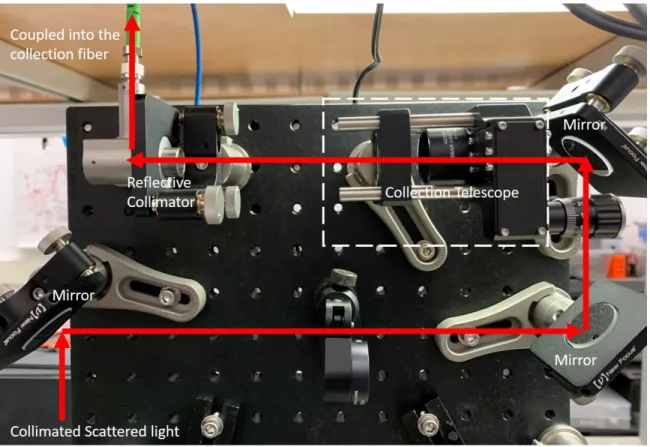
the red arrows indicate the excitation and the collection beam path, respectively. The green arrows and the purple arrows indicate the LED illumination and the reflection imaging beam path, respectively. The components are numbered and are listed in Fig. 2-3. . . 61 2-3 The components in our confocal Raman microscope. The numbers are
labeled in Fig. 2-2. . . 62 2-4 (a) The laser diode packaging and the mounting. (b) The diode driver
and TEC driver. (c) The 99-to-1 fiber tap. (d) The Bristol 621B wavemeter. . . 63 2-5 (a) The input of our setup including the fiber adaptor, the collimator
and the laser clean up filter. (b) The half wave plate (HWP0). The blue arrow indicates the excitation beam. . . 63 2-6 The excitation telescope, the dichroic mirror, and the polarization
se-lection components (HWP+PBC). The blue arrows indicate the exci-tation beam path. . . 64 2-7 (a) The Olympus Objective. (b) The objective Zoomed-in with a
sam-ple under test. The working distance is 350 𝜇m. . . . 66 2-8 The collection optics. The red arrows indicate the collection beam
path. . . 66 2-9 (a) The liquid nitrogen cooled spectrometer. (b) The spectrometer
input from the collection fiber. . . 67 2-10 (a) The imaging optics and the flip mount. The green arrows and the
purple arrows indicate the LED illumination and the reflection imaging beam path, respectively. (b) The LED and its controller. . . 69 2-11 (a) The laser diode packaging and the mounting. (b) The diode driver
and TEC driver. (c) The 99-to-1 fiber tap. (d) The Bristol 621B wavemeter. . . 70
2-12 (a) The piezoelectric scanning stage and the manual stage. (b) The
controller of the piezoelectric scanning stage. . . 71
2-13 The setup to calibrate the strain gauge in the piezoelectric stage using an external gauge. A magnet is used to keep the tip of the nano-gauge in contact with the piezoelectric stage. . . 72
2-14 (a) Displacement readout from the strain gauge and the nano-gauge when the piezoelectric stage is still. (a) Displacement readout from the strain gauge and the nano-gauge when the piezoelectric stage moves in a 100 nm step size. . . 72
2-15 A source-meter used to bias active samples. . . 74
2-16 (a) The AWG trigger. . . 74
2-17 A schematic plot of the optical components. (Gen 1) . . . 75
2-18 Calibration the PSF of Gen 2 in (a) 𝑥 and (b) 𝑦. The inset plots are the optical micrograph of the Au/Si edges. The bright spot is the excitation laser spot. The red arrow indicates the scan direction. The dark region is Si and the bright region is Au. . . 77
2-19 (a) The optical microscopic plot, (b) the SEM of the 2D poly-Si grating. [10] (c) The layer structure of the sample. . . 78
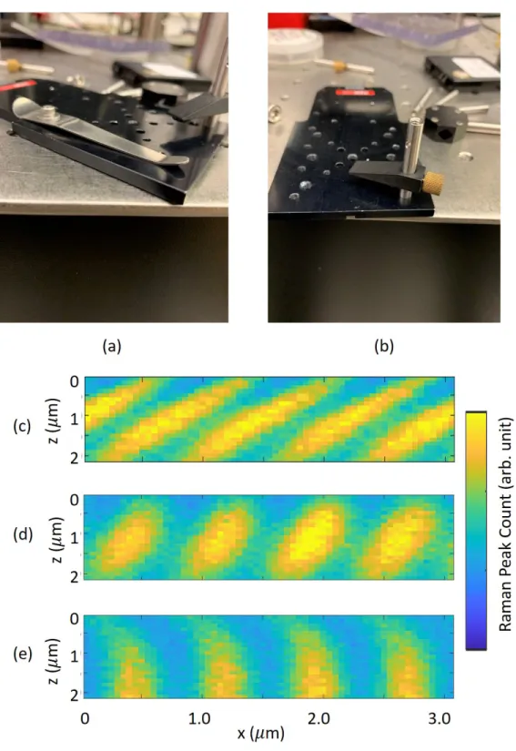
2-20 (a) (b) Two clamps used to hold the samples in the early experiments. (c) (d) (e) Results from 𝑥𝑧 scans with clamps holding the sample. The clamping strength is increased by tightening the screw. Here the 𝑥𝑧 scan is first in 𝑥 then in 𝑧. . . . 80
2-21 The 𝑥𝑧 scan results using different scan patterns. (a) 𝑥 first. (b) 𝑧 first (c) zig-zag. . . 81
2-22 The Si Raman peak count versus time without scanning. The liquid nitrogen tank is refilled at 𝑡 = 0. . . . 81
2-23 The sample is bonded to a small steel board using crystal bond. The steel board is screwed to a rotational stage and the rotational stage is screwed to the 𝑥𝑦𝑧 stage. . . . 82
2-24 The 3D contour surface of the Si Raman peak count from a 3D scan on the 2D poly-Si grating. The contour value is half of the maximum
count. The black curves are the contour lines at each 𝑧. . . . 83
2-25 Slices of the 3D scan in 𝑥𝑦 plane at multiple 𝑧. . . . 84
2-26 Slices of the 3D scan in 𝑥𝑧 plane at multiple 𝑦. . . . 85
2-27 Slices of the 3D scan in 𝑦𝑧 plane at multiple 𝑥. . . . 86
3-1 Comparison of different regularization functions. . . 92
3-2 The model of MCR. [11] . . . 94
3-3 The flowchart of MCR-ALS. [12] . . . 95
3-4 (a) The optical micrograph and (b) the layer structure of the 1D poly-Si grating. The red arrow indicates the scanning direction. . . 97
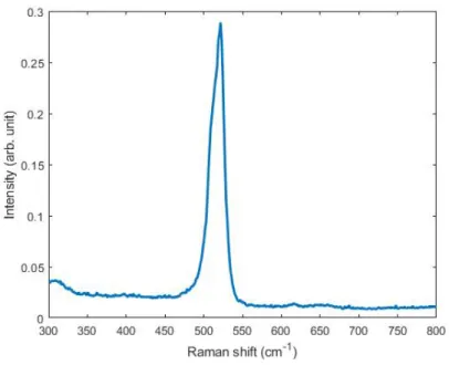
3-5 (a) A typical Si Raman spectrum with the peak located at 518 cm−1. (b) PSF calibration by scanning across the Au/Si edge. The inset plot is the optical micrograph of the Au/Si edge. The red arrow indicates the scanning direction. . . 99
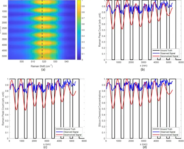
3-6 (a) The raw hyperspectral image of the 1D grating. (b) The Raman peak values at 518 cm−1 versus the position. (c) The estimated Si concentrations from MCR-ALS versus the position. (d)The ground truth of the Si concentrations. . . 100
3-7 Deconvolution results using L2 regularization. 𝜇𝑥 = 0.1, 𝜇𝜆 = 0.1. (a) Deconvolution on the hyperspectral image. (b) the data on the dashed line in (a). (c) Deconvolution using the Raman peak values at 518 cm−1 . (d) Deconvolution using the estimated Si concentrations from MCR-ALS. . . 102
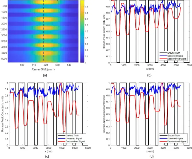
3-8 Deconvolution results using L1 regularization. 𝜇𝑥 = 0.1, 𝜇𝜆 = 0.1. (a) Deconvolution on the hyperspectral image. (b) the data on the dashed line in (a). (c) Deconvolution using the Raman peak values at 518 cm−1 . (d) Deconvolution using the estimated Si concentrations from MCR-ALS. . . 103
3-9 Deconvolution results using L1-L2 regularization. 𝜇𝑥 = 0.1, 𝜇𝜆 = 0.1,
𝜂 = 5 for hyperspectral, 𝜂 = 0.01 for the peak value and concentrations.
(a) Deconvolution on the hyperspectral image. (b) the data on the dashed line in (a). (c) Deconvolution using the Raman peak values at 518 cm−1 . (d) Deconvolution using the estimated Si concentrations from MCR-ALS. . . 104 3-10 Comparison of the deconvolved hyperspectral images with the raw
hy-perspectral images. (a) The raw hyhy-perspectral images. (b) Decon-volution results using L2 regularization. 𝜇𝑥 = 0.1, 𝜇𝜆 = 0.1. (c)
Deconvolution results using L1 regularization. 𝜇𝑥 = 0.1, 𝜇𝜆 = 0.1. (d)
Deconvolution results using L1-L2 regularization. 𝜇𝑥 = 0.1, 𝜇𝜆 = 0.1,
𝜂 = 5. . . . 106 3-11 (a) The optical microscopic plot, (b) the SEM of the 2D poly-Si grating.
[10] (c) The layer structure of the sample. . . 107 3-12 PSF calibration using the waveguide structures in (a)x and (b)y
direc-tion. The bright spot is the laser spot. The red arrow indicates the scanning direction. . . 108 3-13 Singular values of the 𝑥𝑧 scan data set . . . . 109 3-14 Estimated spectrum of poly-Si in the 𝑥𝑧 scan data set . . . . 110 3-15 The Raman images based on the (a)(b) MCR-ALS results and (c)(d)
Si peak intensity. (a)(c) are from the 𝑥𝑧 scan and (b)(d) are from the
𝑦𝑧 scan. The step size is 50 nm in the 𝑥 (𝑦) direction and 100 nm in
the 𝑧 direction. . . . 111 3-16 (a) The half-maximum contour plots of (a)𝑥𝑧 and (b)𝑦𝑧 scan. . . . . 112 3-17 (a) The convolved signal simulated using a PSF FWHM of 400 nm.
(b) The FWHM of the simulated convolved signal versus the FWHM of the PSF. . . 112 3-18 Simulated and experimental convolved signal in the (a)𝑥 and (b)𝑦
3-19 PSF calibration using Au/Si edges in (a)x and (b)y direction. The bright spot is the laser spot. The red arrow indicates the scanning direction. . . 114 3-20 The ground truth and deconvolved signal with varying 𝜇𝑥 based on the
𝑥𝑧 scan data. 𝜇𝑥 = 10−5, 10−3, 10−1, 10. . . . 114
3-21 The FWHM of deconvolved signal versus (a) 𝜇𝑥 and (b) 𝜇𝑦. Given
the FWHM of the ground truth is 550nm, the optimal 𝜇𝑥 = 0.019,
𝜇𝑦 = 0.008. . . . 115
3-22 (a) The hyperspectral image of the 2D grating. The pixels are vector-ized. (b) The image of the Raman peak count at the 518 cm−1channel. (c) The image of the Si concentration from MCR-ALS. (d) The ground truth of the 2D grating. The yellow grid denotes the poly-Si. . . 116 3-23 (a) The MCR-ALS result and (b) deconvolution result of the 2D
poly-Si grating. (c) An 1D slice of data on the red dashed lines in (a) and (b). (d) An 1D slice of data on the yellow dashed lines in (a) and (b). PSF FWHM is 570 nm in 𝑥 and 655 nm in 𝑦. 𝜇𝑥 = 0.008, 𝜇𝑦 = 0.019. 118
3-24 (a) The MCR-ALS result and (b) deconvolution result of the 2D poly-Si grating. (c) An 1D slice of data on the red dashed lines in (a) and (b). (d) An 1D slice of data on the yellow dashed lines in (a) and (b). PSF FWHM is 588.7 nm in 𝑥 and 951.4 nm in 𝑦. 𝜇𝑥 = 0.008,
𝜇𝑦 = 0.019. . . . 120
4-1 (a) The optical micrograph of the TC2 chip. The white dashed box indicates the the region containing L5-1. (b) The optical micrograph of the region containing L5-1. The bright spot is the excitation laser spot. (c) Schematic plot zoomed in the read dashed box in (b). (d) Cross section of the red dashed line in (c). . . 124 4-2 (a) The packaging of the chip with the L5-1 device. (b) The packaging
under test. . . 125 4-3 The IV curve of L5-1. . . 126
4-4 (a) Schematic cross section of L5-1 near the Au contact. PSF calibra-tion on L5-1 in (b) 𝑥 and (c) 𝑦. The bright spot is the excitacalibra-tion laser spot. The red arrow indicates the scanning direction. The calibration is on the same metal line but the sample is rotated 90∘. . . 127
4-5 The Raman spectra at the poly-Si region and the no-poly-Si region with the polarization along (a) ⟨110⟩ and (b) ⟨100⟩ . . . 129
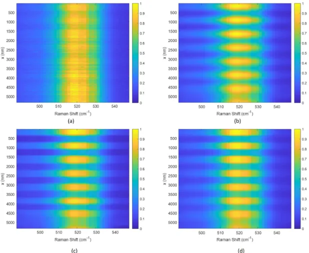
4-6 The Raman images of L5-1 biased at (a) 0 mA, (c) 0.5 mA and (e) 1.0 mA. (b)(d)(f) The Raman spectra near the Si peak in the center and the taper regions, which correspond to the red and the blue circles in (a)(c)(e). There is no polarization selection. . . 130
4-7 The hyperspectral Raman images of L5-1 biased at (a) 0 mA, (b) 0.5 mA and (c) 1.0 mA. The scan is in 𝑧 with 10 𝜇m travel range and 50 nm step size. There is no polarization selection. . . 132
4-8 The hyperspectral images of 𝑧 scan in (a) the poly-Si region and (b) the no-poly-Si region. In the inset plots, the bright spot is the excitation laser spot and the red cross indicates the scanning direction. (c) Blue lines: The poly-Si Raman peak count at the poly-Si region and that at the oxide region versus 𝑧. These lines are on the red dashed line in (a) and (b). Red line: The inverse contrast of the poly-Si Raman peak versus 𝑧. (d) The Raman spectra at the 𝑧 with the maximum contrast. 133
4-9 (a) A 𝑥𝑦 poly-Si Raman peak image on L5-1 at 𝑧𝑚 to find the center
of the device. The polarization is along ⟨100⟩. The images are within 2 × 2 𝜇m2 regions with 50 nm pixel size. (b) A 𝑥𝑦 poly-Si Raman peak
image on L5-1 with no polarization selection. This is the same plot as Fig. 4-6 (a). The images are within 3 × 3 𝜇m2 regions with 50 nm
pixel size. The while dashed boxes indicate the nanowire region. The white dashed triangles indicate the no-poly-Si regions. . . 134
4-10 Hyperspectral Raman images of 1D scan in 𝑦 with bias (a) 𝐼 = 1 mA and (b) 𝐼 = 0 mA. The scanning range is 5 𝜇m and the pixel size is 100 nm. The red dashed lines denote the peak positions. The Raman spectra at 𝑦 = 0, 0.5, 1.0, 1.5, 2.0, 2.5 𝜇m around the poly-Si peak with bias (c) 𝐼 = 1 mA and (d) 𝐼 = 0 mA. The Raman spectra at
𝑦 = 2.5, 3.0, 3.5, 4.0, 4.5, 5.0 𝜇m around the poly-Si peak with bias
(c) 𝐼 = 1 mA and (d) 𝐼 = 0 mA. . . . 136
4-11 The on/off temperature increase versus y using Gen 1.5 at 𝐼 = 1 mA. Here we use coefficient Δ𝑇 = 46 × Δ𝜈 (K). . . . 137
4-12 Hyperspectral Raman images of 1D scan in 𝑧 with bias (a) 𝐼 = 1 mA and (c) 𝐼 = 0 mA with polarization selection. (b) and (d) are same plot as Fig. 4-7 (a) and (c),respectively, without polarization selection. The scanning range is 10 𝜇m and the pixel size is 100 nm. . . . 139
4-13 Hyperspectral Raman images of 1D scan in 𝑥 with bias (a) 𝐼 = 0.5 mA and (c) 𝐼 = 0 mA. The scanning range is 3 𝜇m with 50 nm step size. (c) The fit peak position versus 𝑥. (d) The different of peak position versus position. (e) Lorentzian fitting at 𝑥 = 1450 nm. (f) Lorentzian fitting at 𝑥 = 0 nm. . . . 141
4-14 The workflow of implementing super-resolution in Raman thermogra-phy. . . 142
4-15 (a) The raw Raman spectra at 𝑥 = 1450 nm and 𝑥 = 0 and the background Raman spectrum. (b) The raw Raman spectra at 𝑥 = 1450 nm and 𝑥 = 0 with the background subtracted. . . . 143
4-16 (a) The raw Raman spectra at 𝑥 = 1450 nm and 𝑥 = 0 and the background Raman spectrum. (b) The raw Raman spectra at 𝑥 = 1450 nm and 𝑥 = 0 with the background subtracted. . . . 144
4-17 (a) The fit peak position versus 𝑥. (b) The different of peak position and the temperature increase versus position. The 1 pixel drift from the super-resolution is taken into account. Here we use coefficient Δ𝑇 = 46 × Δ𝜈 (K). (c) The fit peak position versus 𝑥. (d) The different of peak position and the temperature increase versus position. The drift is not considered. . . 145 4-18 Hyperspectral Raman images of (a) 𝐼 = 0.1 mA and (b) 𝐼 = 0 mA.
Super-resolution results of (c) 𝐼 = 0.1 mA and (d) 𝐼 = 0 mA. L1-L2 regularization with 𝜇 = 0.001, 𝜂 = 0.001 are used.(c) The fit peak po-sition versus 𝑥. (b) The different of peak popo-sition and the temperature increase versus 𝑥. Here we use coefficient Δ𝑇 = 46 × Δ𝜈 (K). No drift considered here. . . 146 4-19 Hyperspectral Raman images of (a) 𝐼 = 0.5 mA and (b) 𝐼 = 0 mA.
Super-resolution results of (c) 𝐼 = 0.1 mA and (d) 𝐼 = 0 mA. L2 regularization with 𝜇 = 0.001 is used. (c) The fit peak position versus
𝑥. (b) The different of peak position and the temperature increase
versus 𝑥. . . . 147 4-20 Hyperspectral Raman images of (a) 𝐼 = 0.1 mA and (b) 𝐼 = 0 mA.
Super-resolution results of (c) 𝐼 = 0.1 mA and (d) 𝐼 = 0 mA. L2 regularization with 𝜇 = 0.001 is used.(e) The fit peak position versus
𝑥. (f) The different of peak position and the temperature increase
versus 𝑥. . . . 149 4-21 (a) The wavelength versus the TEC temperature. (b) Stability of the
excitation wavelength. . . 151 4-22 (a) The wavelength versus the TEC temperature. (b) Stability of the
excitation wavelength. . . 152 4-23 (a) The fit Raman wavelength versus the excitation wavelength with
L5-1 biased at 𝐼 = 0.1 mA and 𝐼 = 0 mA. (b) Lorentzian fitting of the shift spectra. . . 153
4-24 (a) The fit Raman wavelength versus the excitation wavelength with L5-1 biased at 𝐼 = 0.05 mA and 𝐼 = 0 mA. (b) The fit Raman wave-length versus the excitation wavewave-length with L5-1 biased at 𝐼 = 0.03 mA and 𝐼 = 0 mA. . . . 155 4-25 A 2D numerical simulation of the on/off temperature increase at the
nanowire. The black line indicates the simulation results. The blue circles are the results from the swept-source measurements with error bars. Here we assume the voltage drop on the nanowire is 0.5 V. The thermal conductivity of poly-Si is 30 W/(m K) [190]. . . 156
5-1 (a) A 𝑥𝑦 poly-Si Raman peak image on L5-1 at 𝑧𝑚 to find the center
of the device. The polarization is along ⟨100⟩. The images are within 2 × 2 𝜇m2 regions with 50 nm pixel size. (b) A 𝑥𝑦 poly-Si Raman peak image on L5-1 with no polarization selection. The images are within 3 × 3 𝜇m2 regions with 50 nm pixel size. The while dashed boxes indicate the nanowire region. The white dashed triangles indicate the no-poly-Si regions. . . 160 5-2 (a) The on/off temperature increase versus 𝑥 with 𝐼 = 0.1 mA. (b)
The on/off temperature increase at the nanowire from the swept-source measurements and a 2D numerical simulation. The black line indicates the simulation results. The blue circles are the results from the swept-source measurements with error bars. . . 161 5-3 The electroluminescent area of L5-1 at 𝐼 = 0.8 mA. (a) The EL colored
image and the Raman contour plot. (b) The Raman colored image and the EL contour plot. In both images, each electroluminescent count is the sum within 880-920 nm and each Raman count is the sum within 817.5-818.5 nm. The contour values are the average of the maximum and the minimum values in the associated images. Here Gen 2 is used with the 600 grooves per mm grating. . . 163
5-4 (a) A photo of the InGaAs pn junction. (b) The epitaxial structure of the pn junction. [158] . . . 164 5-5 Packaging process of the sample. . . 164 5-6 (a) The side view and (b) the top view of the packaged sample. (c)
Top view of the sample after crystal-bonding. . . 165 5-7 The IV curve of the packaged sample. . . 165 5-8 Raman spectra of the pn junction sample from a Renishaw Raman
microscope with 532 nm excitation. . . 166 5-9 The cross section of a leaf [194] . . . 168
A-1 The label on the box containing the Micron D0 sample. . . 172 A-2 An optical micrograph of the the couplers on Micron D0 sample. The
red circle denotes the 1D grating . . . 173 A-3 The poly-Si layer in the GDK file of Micron D0. (b) is a zoom-in of
the red box in (a). (c) is a zoom-in of the red box in (b). . . 174 A-4 The label on the box containing the Micron D-1 sample. . . 175 A-5 An optical micrograph of the the couplers on Micron D0 sample. The
red circle denotes the 2D grating . . . 176
B-1 The sample structure of L5-1. (a) The optical micrograph of the region containing L5-1. The bright spot is the excitation laser spot. (b) Schematic plot zoomed in the read dashed box in (a). (c) Cross section of the red dashed line in (b). . . 178 B-2 (a) The image of the sum of the Raman counts in 506 − 534 cm−1.
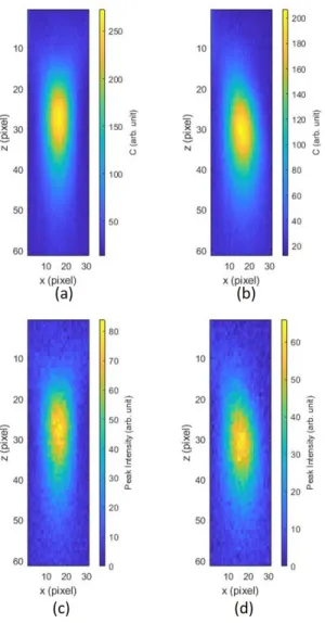
The circles indicate the location corresponding to the Raman spectra in (b). (b) Typical Raman spectra at the taper, the nanowire and the no-poly-Si region. (c) The image of the sum of the dark counts in 880-920 nm . The circles indicate the location corresponding to the spectra in (d). (d) The typical dark spectra at the taper, the nanowire and the no-poly-Si region. The LED is turned off in these figures. . . 179
B-3 (a) The image of the sum of the Raman counts in 506 − 534 cm−1. The circles indicate the location corresponding to the Raman spectra in (b). (b) Typical Raman spectra at the taper, the nanowire and the no-poly-Si region. (c) The image of the sum of the electroluminescent counts in 880-920 nm . The circles indicate the location corresponding to the spectra in (d). (d) The typical electroluminescent spectra at the taper, the nanowire and the no-poly-Si region. The LED is biased at
𝐼 = 1 mA in these figures. . . . 180 B-4 The images of the sum of the electroluminescent counts in 880-920 nm
at (a) 𝐼 = 0, (b) 0.5, (c) 0.7 and (d) 1.0 mA plotted with the contour lines from the corresponding Raman image. The black curves are the contour lines. The contour value is the average of the maximum and the minimum values in each image. The red rectangle of 1 × 2 pixels indicates the estimated position of the nanowire. . . 183
List of Tables
1.1 Comparison of typical nanoscale thermography methods. . . 42 1.2 Comparison of typical Raman Microscopes. . . 50 1.3 Comparison of typical nanoscale thermography methods with
super-resolution infrared Raman thermography. . . 51 2.1 Comparison of Gen 1, Gen 1.5 and Gen 2. . . 76 3.1 Comparison of the estimated teeth width (nm) of an buried 1D grating.
The ground truth is 510 nm from the GDS file. The deviation might come from the error of the estimated PSF FWHM and the shrinkage of the features during the CMOS process. . . 106 3.2 Comparison of PSF FWHM using two different methods. . . 113 3.3 Comparison of the estimated pitch and teeth width of the 2D grating
using different PSFs. . . 119 3.4 Comparison of our deconvolution results with the literature. . . 121 4.1 Raman wavelength shift with 𝐼 = 0.1 mA bias with swept source. . . 154 4.2 Raman wavelength shift with 𝐼 = 0.1 mA bias using single wavelength. 154 4.3 Raman wavelength shift with 𝐼 = 0.05 mA bias with swept source. . 154 4.4 Raman wavelength shift with 𝐼 = 0.03 mA bias with swept source. . 155 4.5 Comparison of our setups with the literature. . . 157 5.1 Comparison of our setups with the literature. . . 161
Chapter 1
Introduction
Reliable tools that perform accurate temperature measurements with nanoscale res-olution are of significant interest, both in industry and in academia. In the modern integrated circuits (ICs) industry, thermal management is a long-standing challenge as the channel length of the field-effect-transistors (FETs) shrinks from over-100 nm to sub-10 nm. [13–18] On the other hand, despite the recent developments of nanotechnology based on novel 1D or 2D materials, fundamental understandings of heat transport processes in the low dimensional spaces are still not completely estab-lished. [17, 19–21] For more than three decades, researchers have put extensive efforts in developing nanoscale thermography tools and have made tremendous progress. [22] For examples, a scanning thermal microscope (SThM) based on an atomic force mi-croscopy (AFM) can achieve 10 nm spatial resolution and 15 mK temperature accu-racy. [23, 24]. Thermoreflectance imaging (TRI), which probes the temperature from the surface reflection, can resolve approximately 10 mK temperature difference at submicron spatial resolution. [25, 26] Lock-in infrared thermography usually has tem-perature resolution of 10 𝜇K and spatial resolution of 5 𝜇m. [27] Raman thermography typically has 1 K temperature resolution and sub-𝜇m spatial resolution. [28–30]
As will be discussed in Section 1.1, all these instruments have their own advan-tages and disadvanadvan-tages in certain situations. Specifically, Raman thermography has multiple advantages as follows. First, Raman thermography directly probes the lat-tice temperature. This eliminates the ambiguity from the impact of the electron
temperature. Second, Raman thermography is a non-contact method which can have minimal perturbation on the probed sample. Third, Raman thermography has the potential of mapping temperature in three dimensional space. Moreover, practically, the instrumentation of Raman thermography is generally simple and the requirements of the samples are relatively flexible. However, Raman thermography has relatively poor temperature resolution and modest spatial resolution compared with other in-struments. In this thesis, we will mainly discuss these limits of Raman thermography and how we improved the performance.
In this introductory chapter, we will first review several typical nanoscale ther-mography setups including scanning thermal microscopy, thermoreflectance imaging and infrared thermography. We will then discuss the basis of Raman microscopy and Raman thermography. Super-resolution techniques will be introduced. Finally, we will elaborate the mechanism and the desired resolutions of Raman themography. As potential applications, self-heating in FinFETs and Peltier cooling in pn junctions will be reviewed.
1.1
Review of Nanoscale Thermography
In this Section, we will review several typical setups for nanoscale thermography.
1.1.1
Scanning Thermal Microscopy
A typical scanning thermal microscope (SThM) is equipped with a temperature sensor integrated into the tip of an atomic force microscope (AFM). [1, 23, 31] (Fig. 1-1 ) Laser reflection and a force feedback loop are usually used to maintain a constant atomic force between the tip and the sample. The mechanism of the temperature sensor can be thermovoltage, [24, 32, 33] temperature-dependent electrical resistance [34, 35] or thermal expansion [36].
SThM generally has outstanding accuracy and spatial resolution. In 2012, Kim et
al. reported SThM under ultra-high vacuum (UHV) that can achieve approximately
Figure 1-1: Schematic SThM setup. [1]
cooling [37], near-field thermophotovoltaics [38], far-field radiative heat transfer over the blackbody limit [39] and quantized thermal transport in single-atom juntions [40, 41] have been observed using the UHV SThM. Despite these milestones achieved, there are multiple practical issues when using SThM. [1] Shi et al. point out the temperature difference between the tip and the sample can be significant due to the finite thermal resistance of the interface. [31] Majumdar et al. suggest one has to at least calibrate the thermal conductance through radiation, gas conduction and water meniscus conduction alongside with the tip-sample direct conduction. [23] Majumdar
et al. also point out the surface roughness can severely affect the local thermal properties. [23] The measurement uncertainty and the spatial resolution of SThM strongly depend on the quality of the tip and the sample. Also, SThM can only probe the surface temperature. In contrast to far-field optical methods, SThM cannot be applied in the situations where the region of interest is buried under other materials or where 3D temperature mapping is required.
Figure 1-2: Schematic TRI setup for (a)measurement and (b)calibration. [2]
1.1.2
Thermoreflectance Imaging
Thermoreflectance Imaging (TRI) is based on the surface reflectance change with temperature as [2, 42, 43] Δ𝑅 𝑅 = 1 𝑅 𝜕𝑅 𝜕𝑇Δ𝑇 = 𝐶𝑇 𝑅Δ (1.1)
where 𝑅 and 𝑇 are the reflectivity of the material and the temperature, respectively.
𝐶𝑇 𝑅 is defined as the thermoreflectance coefficient, which depends on the materials,
wavelength of the probing light and the surface roughness. A TRI setup usually consists of a microscope with light-emitting diode (LED) or laser illumination and a CCD detector. (Fig. 1-2 (a).) The device under test (DUT) is usually modulated at frequency of 1-100 Hz and is phase-locked with the CCD to perform lock-in measure-ments at quasi-equilibrium. Calibration runs are usually required to determine 𝐶𝑇 𝑅
by measuring Δ𝑅 with the sample heated up homogeneously. (Fig. 1-2 (b).)
Currently, TRI can measure approximately 10 mK tempature difference with sub-micron spatial resolution. Efforts have been put into investigating the performance of TRI for the past two decades. Mayer et al. point out that the finite bit-depth of
the CCD does not limit the temperature resolution of TRI with large enough aver-aging images, and that the slow drift of the whole system and the imperfections of the A-to-D converters may be the fundamentally limitations. [2] Kendig et al. dis-cuss the defocusing of the sample due to thermal expansion and use a 3-axis piezo stage to adaptively recapture the sample surface during measurement. [44] Ziabari
et al. used computational methods to reconstruct the thermal images from TRI and
sub-diffraction heater lines of 150 nm can be resolved. [25, 26] Recently, Koskelo et
al. derived a tight upper bound of the temperature resolution given the
quantiza-tion error imposed by the A-to-D converters. [45] TRI is used to analyze thermal performance of microelectronics devices. [43, 46] Variants of TRI such as Time do-main thermoreflectance (TDTR) and frequency dodo-main thermoreflectance (FDTR) are used for studying thermal transport properties of thin film materials and inter-faces. [47–51]
TRI has multiple limitations especially when used for semiconductor samples with submicron features. First, edge effects and local artifacts can severely affect the ther-moreflectance. For example, Dilhaire et al. observed that the parasitic Fabry-Perot modes between the objective and the sample surface can significantly modulate the reflectivity. [52] These Fabry-Perot modes also exist in samples that are buried un-der dielectric layers. Cahill et al. suggest that the sample surface has to be smooth enough with surface roughness lower than 15 nm to avoid diffusive scattering. [17] Cahill et al. also point out that edge effects are usually coupled with the thermoelestic effect. Kendig et al. observed that misalignment of 1 nm can generate major edge effects and these effects are especially severe for sub-micron features. [44] Second, the majority of thermoreflectance work are based on the assumption that different heat carriers, including phonons, photons and electrons, are in equilibrium. [53] Practically, when the system is out of equilibrium, it is usually difficult to separate the thermore-flectance contributions from different heat carriers. For example, besides temperature change, the carrier density change in semiconductors can also lead to the change of the refractive index and the reflectivity. [54] The assumption of equilibrium is ap-proximately valid for metal, but it is generally not true for nanoscale semiconductors.
The assumption can be significantly erroneous for few-layered 2D materials. [55–60] Hence, TIR is primarily used for metal samples. For semiconductors, metal trans-ducers are usually deposited on the samples. Also, rigorous modeling and calibration are required to compute the reflectivity change due to the temperature.
1.1.3
Infrared Thermography
Infrared thermography (IRT) utilizes the Stefan-Boltzmann law which describes that the blackbody radiation power scales with 𝑇4 as
𝑊 = 𝜎𝑇4 (1.2) where 𝑊 is the radiation power, 𝜎 = 5.67 × 10⁻⁸𝑊/(𝑚2𝐾4) is the Stefan-Boltzmann constant. The radiation power can be recorded by infrared detector arrays based on narrow-bandgap semiconductors such as InGaAs and InSb. [61, 61–63] Similar to other CCD-based imaging systems, in order to achieve a high signal-to-noise ratio, it is common to modulate the DUT and perform lock-in measurements. Fig. 1-3 is a schematic example of a IRT with lock-in setup. [3]
Steady IRT and lock-in IRT have temperature resolutions of 10𝑚𝐾 and < 100𝜇𝐾, respectively. The spatial resolution, however, is relatively low and is on the order of a few to tens micronmeters after super-resolution reconstruction. [63] Though IRT is rarely used when nanoscale spatial resolution is required, its high temperature res-olution makes it a powerful tool to visualize extremely small temperature change. For example, Daimin et al. , observed spin-current-induced temperature modula-tion of approximately 0.1𝑚𝐾 using lock-in IRT. [3] Breitenstein et al. quantitatively evaluated shunt defects in solar cell using a lock-in IRT with 0.1𝑚𝐾 accuracy. [64] Breitenstein et al. also present that with a high-speed camera and an on-line aver-aging method, the sensitivity of lock-in thermography can be enhanced to 10𝜇𝐾 and can be used to localize the leakage sites of integrated circuits. [65] Besides the high temperature resolution, IRT also has good scalability and thus is also widely used in medicine manufacturing, agriculture, defense and various other fields. [61–63]
Figure 1-3: A lock-in IRT setup for detection of the spin Peltier effect. [3]
The limitations of IRT mainly come as follows. First, as mentioned above, since the emission is usually in the mid infrared regime, the diffraction-limited spatial resolution is several micrometers. This is approximately 10 times larger compared with TRI or Raman thermography that utilize visible or near infrared excitation. Second, in reality, an observed object is usually a greybody and Eqn. 1.2 should be modified as
𝑊 = 𝜖𝜎𝑇4 (1.3) where 𝜖 is the emissivity varying from 0 to 1. Accurate calibration of emissivity, especially for low emissivity materials, is critical for IRT. In general, the emissivity calibration can be performed either by controlling the object reference temperature or sticking calibration materials with known emissivity to the measured object. [66, 67] Usually, in the calibration steps, naive dependence of emissivity on power and wave-length is assumed. [68] However, this assumption is not suitable in various situation and can leads to severe errors. [69–71] For example, 𝜖 and the carrier density have non-trivial correlation depending on the bandstucture of semiconductors. [54] Third,
IRT need to be operated in a well-controlled environment. The ambient tempera-ture, pressure and moisture all have impact on the measurement accuracy. [61, 68, 71] These factors can significantly complicate the actual experiment setups. Moreover, the infrared camera is usually a costly components. Multiple alternatives have been proposed but the performance is still limited. [62, 68, 72]
1.1.4
Other Methods
There are several other nanoscale thermograpy methods. For example, nanoparticles can be used as thermographic labels because their fluorescent lifetime and intensity have strong dependence on the temperature. [73,74] The transmission and absorption coefficients can be used to extract the temperature if the sample is transparent. [75] For metal surfaces, surface plasmon has information of the thermal properties. [76] However, these methods are either invasive or only have sample-specific applications.
1.2
Raman Microscopy and Raman
Thermogra-phy
In this section, we will first review the basis of spatially resolved Raman spectroscopy and the challenges to obtain high spatial resolutions. we will then review Raman thermography.
1.2.1
Basis of Raman effect and Raman Spectroscopy
The Raman effect refers to the inelastic scattering of photons by molecules. The phenomenon is due to the energy exchange between the incident photons and the vibrational modes of the molecules. [77–79] Fig. 1-4 presents an energy level diagram of this process. Specifically, the molecule is excited to a virtual energy state first by absorbing the incident photon, and then decays to one of its vibrational states by emitting a photon. The scattering process can be elastic and it is named Rayleigh scattering in this situation. Given the scattering is inelastic, if the emitted phonon
has lower energy compared with the incident phonon, the scattering is named the Stokes Raman scattering. Otherwise, it is named the anti-Stokes Raman scattering.
Figure 1-4: The energy diagram of Rayleigh scattering and Raman scattering. The black lines indicate the energy levels. The upward arrows and downwards arrows indicate the incident photons and the scattered photons, respectively.
Raman spectroscopy is a technique to investigate the fundamental properties of materials based on the Raman effect. It has been proved extremely powerful in terms of retrieving information including chemical components, internal stress fields and temperature distributions. [80, 81] Fig. 1-5 is a schematic plot of a typical Raman spectroscopy setup. [82] The excitation source, usually a collimated laser beam, is focused onto the sample to generate the back scattered Raman light. A dichroic mirror and a long-pass filter set is usually used to attenuate the elastic scattered light and the reflected light while transmitting the Stokes Raman light. The Raman light is directed into a dispersive spectrometer, which consists of two collimating mirrors, a reflective grating and a charge-coupled device (CCD) detector. The spectrometer resolves the spectrum of the Raman light.
The readout of the CCD, after binning in one dimension, is a Raman spectrum. In a Raman spectrum, the x-axis is the pixel number or the energy difference between
Figure 1-5: A schematic plot of a typical dispersive Stokes Raman spetroscope. The green and red blocks indicate the incident light and Raman scattered light, respec-tively. The incident and the scattered light is shifted slightly for clearness. The yellow and orange blocks indicate the dispersed components of the Raman light.
the incident and the scattered phonon and is usually described as the Raman shift Δ𝜈 in wavenumber, Δ𝜈 = 1 𝜆𝑒 − 1 𝜆𝑟 (1.4) where 𝜆𝑒 and 𝜆𝑟 are the wavelength of the excitation laser and the Raman light
and Δ𝜈 has the unit cm−1. The y-axis is usually the photon count at each pixel. Sometimes, the photon counts are normalized and thus the y values have arbitary units. This process can be repeat on multiple locations on the sample and a set of spatially resolved Raman spectra are obtained.
1.2.2
Spatial Resolution of Optical Microscopy
The spatial resolution of any optical microscopy, including Raman microscopy, is typically limited by the diffraction limit of the excitation and collection light. Even with perfect optical components, object features smaller than approximately half the illumination wavelength can not be resolved. The diffraction limit Λ𝑚𝑖𝑛 is known as
the Abbe’s limit
Λ𝑚𝑖𝑛 =
𝜆
2𝑁 𝐴 (1.5)
where 𝜆 is the illumination wavelength, 𝑁 𝐴 is the numerical aperture of the objective. Equivalently, any point-like object is imaged with finite size of Λ𝑚𝑖𝑛. The shape of this
blurred image is defined as the point spread function (PSF). The image of an object is the convolution of the object with the PSF of the optical system. As stated by Schermelleh et al. in the context of fluorescence microscopy, ’imaging... is somewhat similar to painting the perfect object structure with a fuzzy brush. The shape of this brush is called the point spread function... ’. [83]
From Eqn. 1.5, it is clear that using shorter wavelength excitation will enhance the resolving power. But as will be discussed later, this may induce unwanted effects such as parasitic heating. It is also possible to have smaller Λ𝑚𝑖𝑛 by increasing 𝑁 𝐴.
1.2.3
Basis of Raman Thermography
Raman thermography extracts temperature from Raman Spectra. The setup is similar to the Raman spectroscope in Fig. 1-5 There are mainly two features can be used to measure the sample temperature. First, due to the dependence of the phonon population on the temperature, the Stokes/anti-Stokes peak intensity ratio depends on the temperature as 𝐼𝐴𝑆 𝐼𝑆 = 𝐶 𝑛 1 + 𝑛 = 𝐶 exp (︃ −¯ℎ𝜔 𝑘𝑇 )︃ (1.6)
where 𝐼𝐴𝑆 and 𝐼𝑆 are the anti-Stokes and Stokes Raman peak intensity, respectively,
𝑛 is the Raman phonon population, 𝐶 is a calibration constant, 𝑘 is the Boltzmann’s
constant, ¯ℎ is the reduced Planck’s constant, and 𝜔 is the Raman frequency shift.
[85, 86] The main advantages of this method is the sample calibration requirement is minimal because the power fluctuation of the excitation laser and the imperfections of the sample such as residual stress are canceled out by the ratio. The primary disadvantage of using the Stokes/anti-Stokes ratio is that an accurate measurement of the peak intensity is challenging. The anti-Stokes intensity can be noisy because of the low phonon population if the Raman shift is not small enough and the Stokes intensity is usually contaminated by fluorescent signal.
The peak position of a Raman mode can also be used to measure the sample temperature. The peak position usually has a linear relationship with temperature as [87]
𝜔(𝑇 ) = 𝐴(𝑇 − 𝑇0) + 𝜔0 (1.7)
where 𝐴 is material-dependent. For single crystal silicon, 𝐴 ≈ −0.025𝑐𝑚−1/𝐾. This
linear dependence reflects that the energy of the associated chemical bond changes with temperature due to the anharmonic potential. Compared with the Stokes/anti-Stokes method, this method has multiple advantages. First, it can be applied for a wider range of materials as long as they have reasonably strong Raman modes. Sec-ond, the linearity within a temperature range of hunderds of 𝐾 makes the
tempera-ture extraction and the calibration straightforward. [87] Also, practically, a longpass dichroic filter can be used instead of a notch filter to extinct the laser reflection, which can further reduce the complexity of the setup. The drawbacks and the limitations of this method are mainly in two aspect. First, the local strain and defects can con-tribute to the peak position change. [30, 88] Although these factors are independent contributors and can be eliminated by calibrations, the temperature-induced effects, such as thermoelasticity in GaN, [30] require more careful treatments. Also, given
𝐴 is a relatively small coefficient, accurate measurement of the peak position is
es-sential for the temperature measurement. The measurement accuracy of the peak position depends on the spectral resolution of the spectrometer. As an estimation, a 1200 grooves/mm grating blazed at 750 nm has a dispersion of approximately 0.7 nm /mrad. Assume the dispersion length of the spectrometer is 250 mm and the CCD pixel width is 20 𝜇m, the dispersion on the CCD is approximately 0.6 cm−1 pixel. This corresponds to about 25K temperature change for 1 pixel peak shift. Therefore, in order to reach K and sub-K accuracy, subpixel peak measurement is necessary. This is usually achieved by fitting the Raman peak to a Lorentzian function.
There are also other features that can be used to measure temperature. For example, the full-width-half-maximum (FWHM) and the intensity of Raman peaks also change with temperature. [87,89] However, these features either have complicated dependence on the temperature (FWHM) or are sensitive to power fluctuation of the excitation (intensity), and thus are rarely reported to be used in Raman thermography in the literature.
1.2.4
Applications of Raman Thermography
In the recent two decades, Raman thermography has been intensively used to study the thermal properties of novel nanoscale materials. For 2D materials and thin films, Raman thermography is usually coupled with an optical heat source. For example, Judek et al. measured the temperature of multi-layer MoS2, graphene and their Si
substrate using a single 514 nm excitation laser both as the heating source and the Raman probe. [90] The thermal conductivity of the 2D materials and the thermal
boundary conductance (TBC) were estimated with statistical uncertainty of approx-imately 2% and 8%, respectively. Using similar setups and procedures with 532 nm excitation lasser, Yalon et al. measured the TBC of single layer MoS2 and substrates
of AlO2/Si and SiO2/Si with uncertainty of approximately 20%. [91] Reparaz et al.
developed the setup and used two lasers, 405 nm and 488 nm, to separate the heat-ing and probheat-ing. [29] They mapped the temperature fields by scannheat-ing the region of interst and computed the in-plane thermal conductivity of Si thin films of differ-ent thickness with ±2 K temperature resolution and 300 nm spatial resolution. The two laser Raman thermography was also used to study the thermal conductivity of periodic and random porous silicon membranes. [92–94] There are also a significant number of reports on the application of Raman thermography in nanowires and quasi 1D materials. For example, by combining SThM and spatial Raman thermography, Soudi et al. studied the heat transport of suspended and supported current-carrying GaN nanowires. [95] The exicitation is 422 nm and the spatial resolution in their work is diffraction-limited. The temperature resolution is approximately 10 K. They concluded that the nanowire-substrate thermal transfer is the main channel of dis-sipating heat and that the thermal conductivity of nanowires is lowered than bulk GaN due to the phonon confinement effect. Majumdar et al. probed the thermal flux in nondefective and twinned Ge nanowires using a 488 nm Ar laser. They observed that the temperature-dependent Raman shift is higher and the thermal conductivity is approximately 10% lower in in the twinned nanowires compared with nondefective nanowires. [96] Similar measurements of thermal conductivity, contact thermal re-sistance and thermal diffusivity have been performed on nanowires based on various materials such as Si, carbon, GaAs and phase changing materials. [97–103] In most of these works, visible excitation lasers are used and the spatial resolutions are on the order of 500 nm. The temperature resolutions in these works are mainly limited by the spectral resolutions which are approximately 0.5 - 1 cm−1. It is claimed in some
reports that after fitting the Raman spectrum to a single Lorentzian or Gaussian function one can locate the peak position with < 0.1 cm−1 uncertainty. However,
Raman thermography is also used to test the performance of active microelec-tronic devices. It is worthwhile to mention that the regions of interest in these devices are usually buried under dielectric materials such as SiN or oxide. Kuball
et al. have published a series of reports on mapping the channel temperatures of
high-power AlGaN/GaN heterostructure field-effect transistors (HFETs) using 532 nm lasers. [28, 104, 104–107] The channels of the HFETs are pasivated by 100 nm SiN. They used a commercial scanning micro-Raman setup which has an excitation spot of 0.5 - 0.7 𝜇m, and frequency shift resolution of 0.1 cm−1, which corresponds to ±5 K temperature resolution for GaN. They concluded that Raman thermography outperforms the traditional electrical temperature determination techniques because of the much higher spatial resolution. They suggested that Raman thermography is especially suitable in the situation that the peak temperatue with the channel is significantly higher than the average channel temperature. Kearney et al. used a 488 nm excitation and reported temperature mapping of electrothermal actuators us-ing Raman thermgraphy with spatial resolution of 1.2 𝜇m and ±10 K measurement uncertainty. [108] Non-trivial stress-induced peak shift as well as multiple source of uncertainty were observed and discussed. Pavlidis et al. compared the thermal per-formance of GaN high-electron-mobility transistors (HEMTs) with and without Si substrates using Raman thermography. [109] They found that the thermal resistance of the GaN HEMTs increases significantly after the substrate removal, which limits the maximum power dissipation. Beechem et al. combined Raman thermography and post-event failure analysis to determine the damaging process of Si pn junctions during laser machining. [110] Their setup is equipped with 532 nm excitaion and an electron-multiplying CCD (EMCCD). The measurement uncertainty was approx-imately 2 − 3 K. Recently, there are also multiple reports on the transient thermal properties of HEMTs using time-resolved Raman thermography. [111–115] In this work, the temporal resolution ranges from < 100 ns to > 10 𝜇s, and their spatial and temperature resolution are similar to the steady Raman thermography.
1.2.5
Heating Issue of Raman Thermography
It is necessary to consider the parasitic heating when using Raman thermography. This is associated with the power and wavelength of the excitation laser. As has been reviewed, most of the reported Raman thermography systems are equipped with visible excitation of 532 nm or 488 nm and no NIR excitation is reported. This is probably due the fact that shorter wavelength excitation leads to a smaller spot size and the Raman signal sclaes with 𝜆−4. [116] However, for minimal parasitic heating when probing the sample, NIR excitation might be more suitable.
In [29], Reparaz et al. discussed the heating process in a thin film sample. For free standing, circular thin membranes of radius 𝑟0 and thickness 𝑑, with a point heating
source at center and a constant 𝑇0 boundary condition, given the absorbed power
𝑃𝑎𝑏𝑠, thermal conductivity 𝜅, the temperature distribution 𝑇 (𝑟) is
𝑇 (𝑟) = 𝑇0 (︂𝑟 𝑟0 )︂−𝑃𝑎𝑏𝑠2𝜋𝑑𝑎 (1.8) for temperature-dependent 𝜅 = 𝑇𝑎 = 𝜅(300𝐾)300𝑇 .
If the excitation power is 𝑃0, and the extinction depth is 𝑡(𝜆) ≫ 𝑑, we can
ap-proximate,
𝑃𝑎𝑏𝑠 ≈ 𝑃0
𝑑
𝑡(𝜆) (1.9)
. Eqn. 1.8, can then be written as
𝑇 (𝑟) = 𝑇0
(︂𝑟
𝑟0
)︂−2𝜋𝑡(𝜆)𝑎𝑃0
(1.10)
Approximately, the Raman intensity is proportional to 𝑃0 and 𝜆−4. [116] If the
Raman intensity is kept the same for different wavelength, it has to be satisfied that
𝑃0 = 𝑃0(𝜆) = 𝑃0(532𝑛𝑚) (︃ 𝜆 532 )︃4 (1.11)
where 𝑃0(𝜆) is the excitation power that generates a certain level of Raman signal.
tem-perature at 𝑟 = 300 nm, where it is roughly the edge of the laser spot. 𝑡(𝜆) can be extraction from [117]. Let 𝑇0 = 300𝐾 and 𝜅(300𝐾) = 1.5𝑊/(𝑐𝑚 · 𝐾). The simulated
temperature versus wavelength is presented in Fig. 1-6. It is clear the parasitic heat-ing is lower as the wavelength increases given that the Raman count is kept invariant. This is mainly due to the fact that the absorption length has stronger dependence on
𝜆 than 𝑃0(𝜆) ∝ 𝜆4. Specifically, 532 nm excitation has 50% more parasitic heating
than 785 nm excitation.
The analysis above does not necessarily confirm that NIR is always better than visible excitation in Raman thermography. Practically, the optimal wavelength also depends on the geometry and the actual sample materials.
Figure 1-6: Temperature rise near the center of a silicon membrane versus the exci-tation wavelength with temperature-dependent 𝜅. Δ𝑇 = 𝑇 (𝑟) − 𝑇0 is computed at
𝑟
𝑟0 = 0.1
1.2.6
Comparison of Nanoscale Thermography
In Table. 1.1, we list the typical resolutions, advantages and shortcomings of the thermography discussed above.
SThM TRI IRT Raman
Mechanism Nanoscale
see-back effect Temperature-dependent reflection Blackbody ra-diation Temperature-dependent peak shift; Stoke/anti-Stokes inten-sity ratio Temperature resolution 10 mK 10 mK 100 𝜇K 2 − 10 K Spatial resolu-tion 10 𝑛𝑚 300 − 500 nm 5 − 10 𝜇m 300 − 500 nm Buried Sample ?
No Yes Yes Yes
Sample pertur-bation ?
Yes minimal minimal moderate
Advantages high spatial
resolution; high tempera-ture resolution non-invasive; high tempera-ture resolution high tem-perature resolution; simple setups non-invasive; directly probe phonon field Limitations complicated calibrations; invasive method cannot directly measure the temperature of semiconduc-tors; nanoscale features induce ambiguity low spatial resolution; complicated calibrations low temper-ature reso-lution; need Raman active modes
with the other techniques presented in Table 1.1. First, the temperature resolution of Raman thermography of 2 − 10 K is poor due to the weak temperature dependence of Raman signals. Second, Raman thermography usually has a spatial resolution that is diffraction limited. Third, during measurement, Raman thermography may perturb the sample temperature because most reported Raman thermography have short wavelength (visible) excitation and the visible excitation can be absorbed by the samples. Also, especially for biological samples, visible excitation is likely to excite autofluorescence.
We point out that the heating issue and the spatial resolution are coupled. As discussed above, the heating issue can be mitigated by using infrared excitation. However, the spatial resolution may be worse due to the longer wavelength. In the next section, we will explore several techniques to surpass the diffraction limit. By using super-resolution techniques, we propose to achieve sub-200nm spatial resolution even when using infrared excitation which has minimal perturbation on the samples temperature distribution.
1.3
Super-resolution Raman Microscopy
In general, techniques used to resolve features lower than the Abbe’s limit are referred as super-resolution. we will review some super-resolution achieved either by modifying the setups or using computational post-processing on the images.
1.3.1
Confocal Configuration
Confocal configuration can be used to enhance the resolution. Nowadays, a typical spatially resolved Raman spectroscope, or Raman microscope, is built in the config-uration of the confocal laser scanning microscopy (CLSM). In CLSM, the excitation and collection focal spots overlap and are usually scanned mechanically by moving the sample on a piezo stage. [118] A schematic plot of a typical Raman microscopy is presented in Fig. 1-7. [4] A pair of pinholes (D1 and D2) are used to block the
If optical fibers are used for the excitation and collection optics, the apertures of the fibers are effectively the pinholes.
Compared with the conventional wide-field microscope, the resolution of a con-focal microscope is better because the PSF is the product of the excitation and the collection PSFs. Empirically, the lateral resolution 𝑟𝐶𝐹 in a confocal system is
𝑟𝐶𝐹 = 0.4
𝜆
𝑁 𝐴 (1.12)
[118].
Figure 1-7: A typical Raman microscope in the configuration of the confocal laser scanning microscopy. [4]
The confocal configuration was originally proposed and patented by M. Minsky in the 1950s for imaging brain tissues. [119] In 1973, Egger et al. reported the ob-servation of endothelial cells using the first reflecive CLSM. [120] The first confocal Raman microscope was built in 1975 by Delhaye and Dhamelincourt. [121] They built multiple configurations to obtain 2D images but the performance was limited by the low intensity Raman signals and the qualities of the optical components at that time. With development of optical fiber manufacturing, laser technology and
computer-controlled spectrum analyzer, nowadays, Raman microscopy has become one of the most powerful tools to spatially analyze various kinds of samples. For example, Wag-ner et al. performed 3D scan of Raman spectroscopy on graphene membranes. [122] The lateral and the axial step sizes are both 300 nm. Freestanding and substrate-supported graphene membranes, as well as their boundaries, can be clearly resolved. Ilchenko et al. demonstrated 2D and 3D mapping of the grain orientations of poly-crystalline materials by scanning polarized Raman microscopy. [123] The lateral and axial step sizes are 0.7 𝜇m and 1.7 𝜇m, respectively. Holmi et al. performed 3D Raman imaging of the volumetric stress distribution in bulk GaN to indentify the threading dislocation types. [124] They used 0.2 𝜇m step size in lateral direction and 1 𝜇m in the vertical direction. Kallepitis et al. reported 3D chemical mapping of biomolecules in multiple cell culture environments using a scanning confocal Raman microscope. [125] They demonstrate the imaging of cytoplasm, nucleus, lipids and glycogen from the same dataset using their Raman fingerprints. The lateral and axial step sizes are 0.65 𝜇m and 1 𝜇m, respectively.
1.3.2
Near-field Super-resolution: TERS
Figure 1-8: A schematic plot of a typical TERS setup. [5]
near-field enhancement to the Raman signal. This configuration is called tip-enhanced Raman scattering (TERS) microscopy. Fig. 1-8 is a schematic plot of a typical TERS setup. [5] In TERS, the spatial resolution is no longer limited by the diffraction limit, but by the size and the sharpness of the tip apex. [126] In multiple recent publications, sub-10 nm spatial resolutions have been reported. Yu et al. reported a spatial resolution of 8 nm on single walled carbon nanotubes (SWCNTs) using a tapping mode AFM to eliminate the far-field background signals. [127] Yano et al. combined TERS with the local tip pressures on SWCNTs and 2D adenine nanocrystal. They demonstrated a spatial resolution of 4 nm. [128] Kurouski et al. used TERS to investigate the structure and composition of insulin fibril surfaces and the spatial resolution is claimed to be approximately 1 nm. There are also reports of TERS having sub-nm resolutions on single molecules, [129, 130] but the mechanism of these sub-nm resolutions is still not fully understood. [5]
Although TERS has proved successful due to the order-of-magnitude enhance-ment of the spatial resolution, there are still drawbacks hindering the applications of TERS in various situations. First, the repeatibility of TERS measurements is usually low. The signal enhancement is extremely sensitive to the morphology of the sample surface and the tip while highly reproducible nanoscale tip fabrication and sur-face preparation are still challenging. [5] Second, the far-field diffraction background severely lowers the contrast of images from SERS and thus complicated techniques such as plasmon nanofocusing or tapping AFM are usualy required. [127, 131] Third, TERS fundamentally can only resolve the features on the sample surface. There is no report on attempting to perform any 3D scan.
1.3.3
Far-field Super-resolution: STED
Stimulated emission depletion (STED) microscopy which was originally built for super-resolution fluorescence microscope [132], has also been proposed for Raman microscopy. In STED microscopy, a donut-shape laser beam generated by a proper phase plate is used to de-excite the fluorophore and prevent them from florescence. The de-exciatation laser spot overlaps with the excitation spot and thus the area of
Figure 1-9: (a) PSF of STED microscopy. (b) PSF size is reduced with the STED beam intensity. [6]
fluorescence, or equivalently, the PSF, is effectively reduced. The reduction of the PSF increases with the intensity of the STED beam due to the saturation effect. (Fig. 1-9 )
The reports on STED spontaneous Raman microscopy are rather limited and the performance is not impressive. This is probably because the depletion of the Ra-man modes requires high intensity of the STED laser. [6] Rieger et al. demonstrated approximately 50% suppression of spontaneous Raman emission at 355 nm by UV laser. [133,134] Based on the experimental results, they claimed a three-fold enhance-ment of resolution in their simulations of the STED Raman. Other attempts of using STED on Raman microscopy are mainly for coherent Raman scattering such as coher-ent anti-Stokes Raman scattering (CARS) [135,136] and stimulated Raman scattering (SRS) [137, 138]. The resolution enhancement in these work is approximately 50%, which is much less effective than TERS.
1.3.4
Far-field Super-resolution: Computational Approaches
Computational approaches can be used to reconstruct the true object from the blurred image. As mentioned above, the image is the convolution of the object and the PSF,𝐼(𝑠) =
∫︁
𝑂(𝑠′)ℎ(𝑠 − 𝑠′)𝑑𝑠′+ 𝑒(𝑠) (1.13) where 𝑠 = (𝑥, 𝑦, 𝑧) is the coordinate of the pixels, 𝐼 and 𝑂 are the intensity of the image and the object at each pixel, ℎ is the PSF, and 𝑒 is the additive noise. This process is illustrated in Fig. 1-10 . [7]
Figure 1-10: The image is the convolution of the object and the PSF. [7]
Eqn. 1.13 can also be written in the matrix form as
𝑌 = 𝐻𝑋 + 𝐸 (1.14) where 𝑌 , 𝑋 and 𝐸 are the vectorized image, object and noise, respectively. 𝐻 is the PSF matrix that
𝐻𝑖,𝑗 = ℎ(𝑠𝑖− 𝑠𝑗) (1.15)
The goal of deconvolution or super-resolution is to reconstruct 𝑋 using the observed
![Figure 1-3: A lock-in IRT setup for detection of the spin Peltier effect. [3]](https://thumb-eu.123doks.com/thumbv2/123doknet/14439577.516666/31.918.201.720.101.486/figure-lock-irt-setup-detection-spin-peltier-effect.webp)