HAL Id: hal-02280377
https://hal.archives-ouvertes.fr/hal-02280377
Submitted on 6 Sep 2019
HAL is a multi-disciplinary open access
archive for the deposit and dissemination of
sci-entific research documents, whether they are
pub-lished or not. The documents may come from
teaching and research institutions in France or
abroad, or from public or private research centers.
L’archive ouverte pluridisciplinaire HAL, est
destinée au dépôt et à la diffusion de documents
scientifiques de niveau recherche, publiés ou non,
émanant des établissements d’enseignement et de
recherche français ou étrangers, des laboratoires
publics ou privés.
Abderrahim Azzoune, Philippe Delaye, Gilles Pauliat
To cite this version:
Abderrahim Azzoune, Philippe Delaye, Gilles Pauliat. Optical microscopy for measuring tapered
fibers beyond the diffraction limit. Optics Express, Optical Society of America - OSA Publishing,
2019, 27 (17), pp.24403-24415. �10.1364/OE.27.024403�. �hal-02280377�
Optical microscopy for measuring tapered fibers
beyond the diffraction limit
A
BDERRAHIMA
ZZOUNE,
*P
HILIPPED
ELAYE,
ANDG
ILLESP
AULIAT Laboratoire Charles Fabry, Institut d’Optique, CNRS, Université Paris-Saclay, 91127 Palaiseau cedex, FranceAbstract: We describe a technique that allows the improvement of the resolution of optical
microscopes for nanofiber measurements beyond the diffraction limit. It can be readily imple-mented on any microscope. We demonstrated it by measuring tapered fibers radii from 0.4 to 4 µm with a resolution below the diffraction limit, from a few nanometers up to 50 nm in the worst case, depending on the radii. This technique is a non-contact measurement with the microscope objective placed a few centimeters from the nanofiber. We acquire the experimental diffraction pattern by scanning the object plane of the microscope system, upstream and downstream the nanofiber. We compare this experimental diffraction pattern to a bank of all the simulated patterns for all the radii. The radius of the simulated diffraction pattern that best matches to the experimental one is the sought radius.
© 2019 Optical Society of America under the terms of theOSA Open Access Publishing Agreement
1. Introduction
Optical micro and nanofibers received considerable interest for studying optical nonlinear interactions or for conceiving optical sensors [1,2]. These nanofibers can be obtained via flame-brushing techniques [3,4], typically from a telecom fiber whose diameter is 125 µm. A heater softens a section of this fiber, while its two ends are pulled apart. The resulting object is a nanofiber with an extremely large aspect ratio: its diameter can be below one micrometer while its length can easily exceed several centimeters. This nanofiber is attached by two tapered transition sections to the original standard fiber. A precise computer control of this pulling process allows a full design of the nanofiber and the tapered sections [5,6]. The obtained waveguide possesses fascinating properties. It can be readily and efficiently connected to the outside world (fiber networks or experiments) by the two untouched fiber sections. The overall optical transmission, including the two tapered sections and the nanofiber, can exceed 99% [7]. The natural light concentration produced by these tapers favors nonlinear effects [8–10]. The strong evanescent optical field in the nanofibers section makes the light propagation very sensitive to the external environment. These features serve as the basis of a full variety of optical sensors [11,12]. They have been used for stimulated Raman scattering in the evanescent field [13,14], in four wave mixing [10,15,16], for correlated photon sources [17], as well as in quantum optics [18,19] and optomechanics [20].
The counterpart of this ease of fabrication is an imperfect knowledge of the device profile, i.e. its diameter versus the light propagation axis. Indeed, device optimization may require an extremely accurate knowledge of this profile. As an example, in a silica nanofiber, phase matching for second harmonic generation can be obtained from a fundamental mode HE11at 1550 nm towards a higher mode TM01at 775 nm if the nanofiber diameter is 693 nm [21]. Efficient second harmonic generation in a 100 µm long nanofiber requires this diameter to be maintained with an accuracy of ± 20 nm. Measuring the profiles with such accuracies is highly demanding and, is not directly accessible with conventional optical microscopy. Although scanning electron microscopy (SEM) could be used to measure such profiles, this is a destructive method: the clamping of the nanofiber on the measurement substrate and the gold deposit required for SEM
#364102 https://doi.org/10.1364/OE.27.024403
measurements are irreversible actions. Once measured, the nanofiber cannot be used any further. Furthermore, reaching a nanometer accuracy with electronic microscopy is very challenging. Therefore, simple non-destructive techniques for measuring the profile of nanofibers should be developed. A full panel of methods have indeed been developed over the years. Scanning a stripped fiber along the nanofiber allows measuring the uniformity with a precision of 2% [22]. This technique gives a deep insight on the fiber profile with the minimum assumptions. However, this technique is not straightforward to implement. It requires to position the probe fiber in contact with the nanofiber, and typically can hardly be used to monitor the nanofiber diameter during the pulling process. Others [23–27], provide the fiber profile but with a limited resolution along the fiber axis. Although quite accurate, other techniques [28–30] do not provide access to the full fiber profile. They just give access to its mean value integrated over the nanofiber length or to its minimum diameter. Furthermore, most of these techniques are indirect measurements, in the way that they require a complex model to link the measurements (Rayleigh, Brillouin scattering, etc.) to the nanofiber diameter.
For these reasons, we have developed a straightforward technique to measure the nanofiber profile with a resolution beyond the diffraction limit along the diameter and of a few micrometers along the nanofiber axis. This is a non-contact technique that uses a conventional optical microscope and that can be directly mounted onto the pulling rig. The resolution of standard microscopy is limited by the diffraction, typically to about λ/NA, so about 1 µm in the visible range and with a numerical aperture NA= 0.42. Moreover, the object is transparent and thick with no sharp edges. It is nearly impossible to focus precisely the microscope in a specific plane, for instance the plane containing the nanofiber center. Nevertheless, it is well known that this diffraction limit can be beaten by various super-resolution techniques. We developed such a technique that does not require any change in the microscope but just rely on an a priori knowledge of the object to be measured, and on numerical processing. The diffracted pattern of light scattered onto the experimental nanofiber, whose diameter is to be determined, is captured by the microscope. This experimental diffraction pattern is then numerically compared to a set of reference images computed by modelling the light diffraction by nanofibers and its propagation through the microscope until its acquisition by the microscope camera. These reference images are computed for various nanofiber radii, the pitch between two successive radii depending on the desired resolution on the radius determination. The reference image that presents the best match with the experimental diffraction pattern gives the experimental radius.
2. Optical microscope configuration
2.1. Experimental arrangement
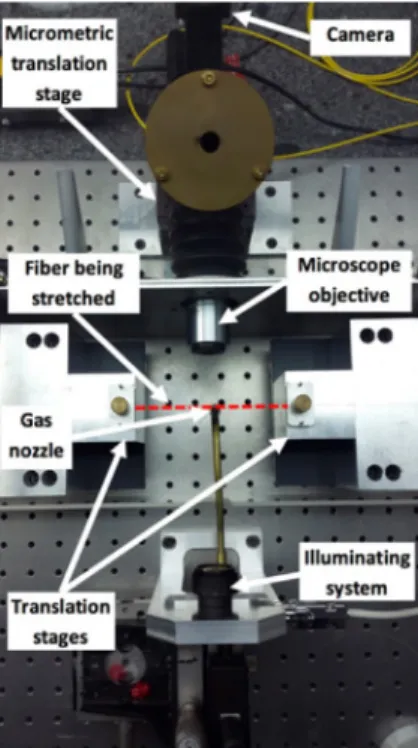
We draw nanofibers using the pulling rig shown in Fig.1[31]. This rig is assembled onto a metallic breadboard itself laid on a massive granite optical table. We start from standard telecom (SMF28) fibers attached to the two translation stages. The trajectories of the two stages are computer controlled. The heater is a butane flame. We use the well-known “heat-brush” pulling procedure to precisely reach the desired shape of the nanofiber [32]. In principle, with such a technique, the nanofiber shape only depends on the translation stage trajectories and is thus reproducible. In the real word, uncertainties, such as butane flame fluctuations make the nanofiber profile slightly depart from the targeted one. Hence the need for a post-fabrication measurement.
As shown in this Fig.1, we implemented a conventional optical microscope to visualize the nanofiber onto the rig. We selected the bright field imaging arrangement. The nanofiber is illuminated from one side and observed on the other one. As light source, we selected a LED emitting at 462 nm, instead of a Laser, in order to avoid too speckled images. The spectrum of the collected light is narrowed by an interference filter set inside the microscope itself. The LED light is polarized along the fiber axis, the other polarization has been tested and it doesn’t give more information. The LED is set at a long distance from the fiber, so that the beam at the
Fig. 1. Photograph of the pulling rig; the dashed red line represents the nanofiber.
nanofiber can be approximated by a plane wave. We checked that the nanofiber illumination is uniform to within better than 10%.
In our experiment we use the following parameters: • distance between the LED and the nanofiber, 20 cm;
• microscope objective x20, infinity corrected, plan apochromatic, with a numerical aperture of NA= 0.42, and a long working distance of 20 mm (from Mitutoyo);
• tube lens focal length f= 20 cm;
• Grasshopper3 camera GS3-U3-32S4M-C from PtGrey, with 2048 × 1536 pixels whose sizes are 3.45 × 3.45 µm2.
An experimental calibration of the microscope gives a measured magnification of G= 20 ± 0.25 corresponding to one pixel every 172.5 nm ± 2 nm in the nanofiber plane. In between the microscope objective and the tube lens, we inserted the interference bandpass filter. The transmitted spectrum is centered around λ = 462 nm with a full width at half-maximum ∆λ = 9.0 nm. The full microscope, “objective – filter – tube lens – camera”, is installed on a motorized linear translation stage moving along the microscope axis with an incremental motion of 50 nm. The whole pulling rig is set in a dust free environment, and a plastic cover protects the nanofiber from air turbulences. Before any measurements, we pay special attention to align the nanofiber, the LED and the translation displacement along the line of sight of the microscope. The gamma correction of the camera is set to unity, and its offset is corrected in order to get a signal proportional to the number of photons.
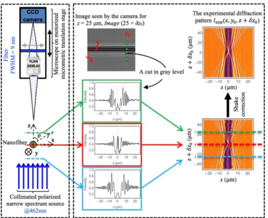
2.2. Image acquisition
Although we can move the microscope from one focusing plane to another with the high precision translation stage, the absolute position of these planes relatively to the nanofiber center is unknown by an amount δz0. δz0 is lower or about the depth of focus of our microscope. In order to overcome this limitation, and to determine the nanofiber radii with a few nanometers resolution, we have decided to collect the diffracted intensity within a volume extending over
x, y and z ; y being the coordinate along the fiber axis, z being the aiming line, and x the coordinate perpendicular to the (y, z) plane (see Fig.2). The origin of the coordinate system is set at the nanofiber center. Acquiring the diffracted intensity versus z suppresses the problem to experimentally determine the absolute position of the focus plane with respect to the fiber center, that is the shift δz0. This shift will be determined after the acquisitions are done, by analyzing the data. Furthermore, acquiring the intensity over a volume provides redundant information. This will contribute to improve the resolution.
Fig. 2. Left: Scheme of the microscope and its illuminating system; the nanofiber is
perpendicular to this figure, along y-axis; its center corresponds to point 0, the origin of system (x, y, z). Right: Illustration of the procedure used to reconstruct the experimental diffraction pattern Iexp(x, y0, z+ δz0) starting from a series of camera acquisitions Image (z+ δz0) (see text).
To assure that the acquired diffraction intensity fully overlaps the simulated pattern, we acquire this intensity over a range [− ∆z+ δz0;+ ∆z + δz0] in z larger than the simulation range. To do so, we take a series of 200 images, Image (z+ δz0), by changing the focus by steps of 0.5 µm starting from zstart= − 50 µm + δz0to zstop= zstart+ 100 µm. We then select a given position
y0along the nanofiber at which we desire to determine the diameter. From each image of the series of 200 images, Image (z+ δz0), we extract a profile along x-axis. Three such experimental
profiles are shown as an example in the middle of Fig.2. All these 200 profiles are stacked together to produce the diffraction image shown at the bottom right of Fig.2. The imperfect alignment of the profiles against each other reflects the movement of the nanofiber. It is indeed suspended in the air and free to move along the x- and z-axes. To minimize these movements, before radius measurements, we always tighten the nanofiber by slightly pulling apart the two translation stages. From this image shown at the bottom right of Fig.2, we estimate that it moves over a distance whose standard deviation is less than 0.5 µm in both directions, lower than the microscope depth of field. We then numerically correct this shake: each profile is centered around x= 0 by maximizing the correlation between its left and right parts. After this shake correction we obtain the diffraction pattern Iexp(x, y0, z+ δz0) shown on the top right of Fig.2.
This is this image that we are going to compare to the simulated diffraction patterns to determine both the shift δz0and the nanofiber radius.
3. Modelling the diffraction pattern
Our aim is to measure the nanofiber profile a(y), that is the radius variation along y-axis. For that purpose, we consider that around each point y0the nanofiber is a circular cylinder made of fused silica. We thus assume the diameter to be uniform over a small length δy around y0. In other words, diameter measurements for two coordinates spaced by more than δy are independent: δy is the resolution of our technique along the nanofiber axis. It is given later in this paper.
We now focus in the diameter determination for a specific y0. The pattern simulation procedure is illustrated in Fig.3, the incident optical field on the nanofiber is a plane wave propagating from − z to+ z. The incident polarization being along y-axis, the fiber axis, it remains unchanged by interacting with the nanofiber. We rely on the exact expressions of the electric field E(r, θ) in cylindrical coordinates derived in the literature [33]. This electric field for r > a, i.e. outside the nanofiber, is E(r, θ)= +∞ Õ m=−∞ i−mexp(imθ)[Jm(kr) − bmHm(kr)], (1) where bm=
nJ0m(nka)Jm(ka) − Jm(nka)Jm0(ka)
nJ0m(nka)Hm(ka) − Jm(nka)Hm0(ka)
, (2)
and (inside the nanofiber) for r < a
E(r, θ)= πkr2 +∞ Õ m=−∞ i−m+1exp(imθ)amJm(nkr)= M Õ m=1 amTM0mG, (3) where am= 1
nJ0m(nka)Hm(ka) − Jm(nka)Hm0(ka)
, (4)
Jmrepresents the Bessel function of the first kind, Hmthe Hankel function of the second kind
and the prime indicating their derivative, n the silica refractive index [34], (r, θ) the cylindrical coordinates as shown in Fig.2and k= 2π/λ the wave number. The notations TM0mGstand for the magnetic transverse gallery modes of order m. For the simulations, the infinite summation is truncated, resulting in a compromise between the computation time and precision. Typically, we use a total of a few hundred terms.
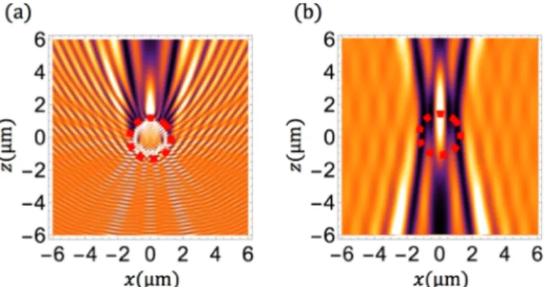
As an example, in the Fig.3(a) we simulated the total intensity for a nanofiber whose radius is
a= 1 µm. This intensity is defined as the refractive index times the modulus square of the electric
field. The nanofiber is in the middle of the plot that extends over [− 6 µm,+ 6 µm] along both x-and z-axes. For z < a one observes some ripples on the incident plane wave originating from light back-reflected by the nanofiber. The bright spot at x= 0 corresponds to the focal point of the nanofiber that acts as a cylindrical lens (sometimes called “nanojet” in the literature).
Fig. 3. Patterns simulation procedure; red dashed circle represents the nanofiber. (a) Total
intensity for a nanofiber whose radius is a= 1 µm, calculated using Eq. (1) and Eq. (3); for z < a: ripples on the incident plane wave originating from light back-reflected by the nanofiber. (b) Intensity captured by the camera, take a field at z0= a: propagation by plane wave decomposition limited by microscope aperture (0.42); for z < a: plane wave seen through the nanofiber.
This image, in the Fig.3(a), represents the intensity inside and around the nanofiber. However, this is not the intensity as captured by the microscope camera. This camera indeed captures the optical waves that are filtered by the microscope numerical aperture and that are distorted by their propagation through the nanofiber diopters (for z < a). To compute the intensity captured by the camera, we first compute the optical field along a given single line z0with z0≥ a relying on Eq. (1). This position z0is arbitrary. Provided it remains larger than the nanofiber radius, it does not affect the result. In our simulation we have taken z0= a. Once we know the field in this plane, we can now propagate it in any other plane. For this propagation we have selected a plane wave decomposition limited to the numerical aperture NA of the microscope. We conduct the development in a Cartesian coordinate system, the spatial coordinates of vector r at which the field is calculated are (x, y0, z) and the spatial coordinates of vector r0at which the field is decomposed are (x, y0, z0). We can write
E(r) ∝ p=P Õ p=−P cpexp(ikp.r), (5) where cp(y0, z0) ∝ +∆x ∫ −∆x E(r0) exp(−ikp.r0)dx. (6)
For sake of symmetry, all wave vectors kpof the plane wave components, have a zero projection
along the y-axis
kp= {k sin[α(p)], 0, k cos[α(p)]}, (7)
where α(p)= (p/P) arcsin(NA). The number of samples, 2P + 1, is selected so as to correctly sample the image field used to determine the radius. To avoid artifacts on the border of the window [− ∆x;+ ∆x], we conduct our computation on 2.5 times the size of this observation window, which gives P ≥ ∆x/δx where δx is the desired sample spacing.
The pattern shown in the Fig.3(b) is the result of such a procedure. It corresponds to the intensity captured by the camera, that is after their propagation through the nanofiber and filtering by the numerical aperture of the microscope. The plane wave aspect for z < a is obviously no
more visible as this figure represents the intensity seen by the camera and thus deformed by light propagation through the nanofiber. Similarly, the slanted fringes are the result of diffraction by the microscope objective aperture. Their number and slant change with the numerical aperture value.
To take into account the finite width of the (LED+ filter) spectrum, we incoherently add-up ten such patterns simulated for the same radius, but with wavelengths equally spaced over the (LED+ filter) spectrum bandwidth.
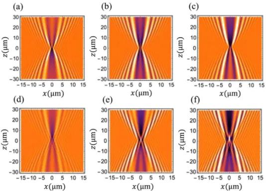
Using these simulations for the (LED+ filter) spectrum, we then computed a bank of diffraction patterns Pattern(a) for a comb of radii a. The spacing between successive radii, is chosen according to the targeted resolution on the radius determination. Hereafter, it is equal to 1 nm for radii ranging from 0.2 to 4 µm. These patterns are computed over a [− 15 µm;+15 µm] observation window along the x-axis and [− 30 µm;+ 30 µm] along the z-axis. Some diffraction patterns are shown in Fig.4. Samplings along the x- and z-axes are the same as those of the experimental images: 0.1725 × 0.5 µm2.
Fig. 4. Simulated diffraction patterns. (a) a= 0.2 µm. (b) a = 0.3 µm. (c) a = 0.4 µm. (d) a= 0.5 µm. (e) a = 1.0 µm. (f) a = 1.5 µm.
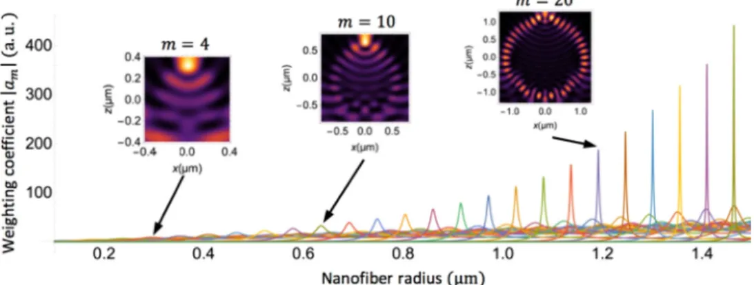
These diffraction patterns change significantly for changes of the nanofiber radius even smaller than the wavelength. For example, see patterns shown in Figs.4(b) and4(c). They can thus be seen as “fingerprints” of the various radii. Theses quick changes can be readily understood by examining Eq. (3). Light inside the nanofiber, which is responsible for the diffraction pattern outside the nanofiber, can be decomposed on the basis of gallery modes TM0mG. The weighting coefficients |am| of the first 25 gallery modes are shown in Fig.5for λ= 462nm.
This figure illustrates the strong resonances experienced by the gallery modes. Each mode has a specific resonance. They are spaced by about 50 nm. These resonances explain why the diffraction patterns vary significantly even for changes in radius smaller than the wavelength. This also explains why measurement precision varies with the radius every 50 nm or so, as we will see in section5.
Fig. 5. Weighting coefficients |am| of gallery modes TM0mGexcited inside the nanofiber; the inserts represent the total intensity inside and surrounding the nanofiber for radii corresponding to the resonance of the TM04G, TM010Gand TM020Ggallery modes.
4. Radius determination procedure
The experimental diffraction pattern Iexp (x, y0, z+ δz0) is the query image that we want to
compare with all the diffraction patterns Pattern(a), in order to determine the nanofiber radius. A visual comparison already allows us to determine the radius with an estimated resolution of about 100 nm, for radii around 1 µm [35]. To go further we have decided to automate this procedure using known image processing techniques by computing the image distances between the experimental diffraction pattern and the set of simulated ones. The radius corresponding to the minimum distance will be the sought radius.
To do so, we first normalize all experimental and simulated patterns to the intensity taken in an unperturbed region, typically on the x borders. We have to determine the two unknowns in the experimental image: fiber center position δz0and radius a. To this end, we introduce a new notation Iexp(x, y0, z+ δz0−δz) that corresponds to the experimental pattern that we have
shifted by an amount δz along the z-axis. This shift δz is used to compensate and determine the unknown δz0. This shifted pattern Iexp(x, y0, z+ δz0−δz) is then cropped to fit the same window as the simulated patterns.
Among the various image distance metrics, we have selected the Euclidean distance. We need to compute this image distance between the shifted experimental diffraction patterns Iexp
(x, y0, z+ δz0 −δz) and Pattern(a) for all radii a and for each possible shift value δz. To get
good estimates, we selected a spacing between two successive shifts equal to the sampling of the experiment image, that is 0.5 µm. The Euclidean distance is defined as
Dist(a, δz)= s
Õ
p
[Iexp,p(δz) − Patp(a)]2, (8)
where summation over p stands over the intensities of all pixels; Iexp, p(δz) are the pixel intensities of the query shifted diffraction pattern Iexp(x, y0, z+ δz0−δz), and Patp(a) are the pixel intensities
of the simulated reference pattern Pattern(a). The simulated diffraction pattern Pattern(a) and shifted experimental Iexp(x, y0, z+ δz0−δz) one for which the distance is minimal correspond to
the sought radius a and shift δz= δz0.
5. Experimental results and discussion
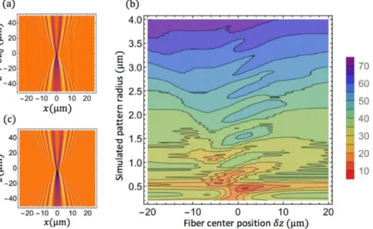
We then draw a nanofiber and acquire the corresponding experimental diffraction pattern for a given position y0along the nanofiber. It is shown in Fig.6(a). We compute the Euclidean
distances between the shifted versions of this experimental diffraction pattern and the set of simulated ones. The distances are then arranged under the form of a distance map as a function of all possible radii a and shift δz, see Fig.6(b). The radius corresponding to the absolute minimum distance is the sought radius. The best matching for this nanofiber is for a= 0.451 µm and δz = 2 µm. For a visual verification, we simulated a pattern for this found radius and over the same window as the experimental one (see Fig.6(c)). This visual comparison is fully satisfactory.
Fig. 6. Simultaneous determination of fiber focus position and radius. (a) Experimental
diffraction pattern. (b) Image distances between the experimental diffraction pattern and the set of diffraction patterns calculated for all the radii and shift δz; best matching for a= 0.451 µm and δz= 2 µm. (c) Simulated diffraction pattern for a visual verification.
The pseudo-periodic modulation visible in the distance map of Fig.6(b) along the radius axis (appearance of lines parallel to the δz axis) is due to the periodic excitation of our gallery modes as radius a increases. We will discuss this feature later in this paper.
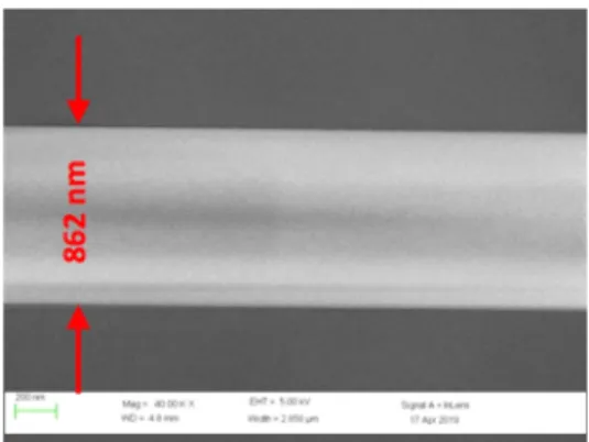
To appreciate the accuracy of our technique, we compared previous measurements in Fig.6
with SEM measurements (see Fig.7). This SEM measurement gives a radius of 431 nm; this value perfectly agrees within uncertainties with our measurements of 451 nm.
This SEM image also illustrates the high quality of the surface of the nanofiber without visible surface roughness. This reinforces our assumption of modelling the nanofiber by a perfect silica rod.
Such SEM measurements were performed on different sections of the nanofiber and on two different nanofibers for radii in the range 400 nm - 500 nm. These results are always in perfect agreement: the standard deviation of the difference between the optically determined radii and the SEM determined radii is 26 nm.
This radius measurement can be replicated for any position y along the nanofiber, allowing to determine the full nanofiber profile a(y). In an image plane, the microscope resolution along
y-axis is about λ/(2NA). However, we acquire images out of focus for determining the nanofiber radius. This gives an upper limit on the resolution ∆y along y-axis
Fig. 7. SEM measurement of the same nanofiber measured in Fig.6with our technique.
∆zbeing the maximum out of focus. In our experiment, ∆z= 30 µm and NA = 0.42, the resolution along y-axis is thus bounded by ∆y ≤ 25 µm.
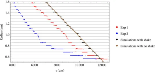
We present in Fig.8, the profiles of two nanofibers measured by this technique.
Fig. 8. Fiber profiles measured by this technique.
It is worth noting that the time required to compute the map in Fig.6(b) for a single point is relatively lengthy, typically a few tens of seconds on a desktop computer. However, computing the radius for successive points along the fiber axis can be considerably speed-up because the approximate radius and fiber center position are known to be similar to the previous point. The search area is thus considerably reduced.
These profiles present a staircase structure for low radii, with a step height of about 50 nm, that reflects the main source of error as explained in the following paragraph. This structure is not present for large radii.
To better understand the origin of errors, we enlarge in Fig.9part of the profiles previously shown in Fig.8. On this enlarge scale, the staircase structure is more visible. A noticeable feature of this structure is that it is absolutely reproducible from one profile to another one. Whatever the nanofiber, whatever the set-up alignment, the steps are always located at the same radii and spaced by about 50 nm.
To determine the origin of these steps, we decided to completely simulate the experiment and to introduce various “defects” one after the other one until we are able to reproduce these steps.
Fig. 9. Zoom on the fiber profiles shown in Fig.7with two simulated ones including or neglecting the fiber movement. The horizontal grey lines correspond to the radii of resonances of the gallery modes (Fig.5). The y offsets between the different curves is chosen for clarity and is not relevant, except for the two simulated curves that were modelled starting from the same nanofiber profile.
We studied the influence of the discretization of the acquired and simulated patterns along x- and
z-axes by simulating cameras with smaller pixels; we tested reference pattern spacing smaller than 1 nm; we tested the influence of errors on the microscope magnification; the influence of the camera offset, of the camera detection noise, of the scattered light inside the microscope; we evaluated the influence of an imperfect image normalization and of an imperfect set-up alignment. We found that the cumulated effect of all these “defects” introduces an error on the radius determination lower than 5 nm.
The last source of error originates from small movements of the fiber that is suspended in the air. Although the fiber does not move during the camera acquisition time, the time require to collect a full series of images, see Fig.2, can be up to a few minutes during which the fiber moves. If we can partly correct this shake along the x-axis, we cannot do it along the z-axis. We thus simulated a nanofiber whose radius changes linearly along the fiber axis. For each position along this axis we simulated noise shake due to the fiber movement with about the same statistics as the one measured experimentally. We then proceeded at the automated radius determination. The corresponding profile is shown in black in Fig.9. The simulated one for the same linear profile with no shake is presented in brown in Fig.9to verify our approach. For this last simulation the radii found by the procedure correspond to the ones used for the simulation.
This simulation with shake evidenced the same staircase structure as the experimental profiles, with the same radius hops, located exactly at the same radius positions: every 50 nm as for the resonances of the gallery modes. For radii above 2 µm, this structure disappears leading to a better resolution. This better resolution for higher radii could be attributed to the higher order gallery modes excited for larger diameters (see Fig.5). The diffraction patterns are thus more complex for large radii, and thus more easily discernable.
We thus conclude that the resolution of this technique is limited by noise due to the fiber movements. This resolution is radius dependent but is always better than 50 nm. To get the best resolution, especially for small radii, the fiber movements must be reduced as far as possible.
6. Conclusion
We described a simple method to improve the microscope resolution for nanofiber measurements beyond the diffraction limit. Although we validated this method by measuring nanofiber radii ranging from 0.4 to 4 µm, extending the measurements over larger ranges is straightforward. From simulations, and taking into account the measured noise levels, we also conclude that measurements in the range 0.2 to 0.4 µm should be possible. The strengths of this technique are as follows: it is inexpensive and relatively easy to implement on existing microscopes. It can be implemented on the pulling rig without any manipulation of the nanofiber. It allows an extended range of diameter measurements. It provides a diameter measurement at each point along the nanofiber. The precision is presently 50 nm peak to peak in the worst case depending on the fiber radius. This compares very favorably with the diffraction limit that is 1 µm.
The resolution is limited by the fiber movements that produce radius hops occurring around each gallery mode resonance. This feature suggests that operating the same technique at various wavelengths, for which the resonances occur at different radii, should allow a further improvement of the resolution.
Funding
Agence Nationale de la Recherche (FUNFILM-ANR-16- CE24-0010-03); Algerian Ministry of Defense (MDN/ANP).
Acknowledgments
The authors would like to thank Anne-Lise Coutrot for SEM measurements. A. A. is so grateful to the Algerian Ministry of Defense for granting his scholarship.
References
1. L. Tong, R. R. Gattass, J. B. Ashcom, S. He, J. Lou, M. Shen, I. Maxwell, and E. Mazur, “Subwavelength-diameter silica wires for low-loss optical wave guiding,”Nature426(6968), 816–819 (2003).
2. L. Tong, J. Lou, and E. Mazur, “Single-mode guiding properties of subwavelength-diameter silica and silicon wire waveguides,”Opt. Express12(6), 1025–1035 (2004).
3. T. A. Birks and Y. W. Li, “The shape of fiber tapers,”J. Lightwave Technol.10(4), 432–438 (1992).
4. R. P. Kenny, T. A. Birks, and K. P. Oakley, “Control of optical fibre taper shape,”Electron. Lett.27(18), 1654–1656 (1991).
5. A. Felipe, G. Espíndola, H. J. Kalinowski, J. A. S. Lima, and A. S. Paterno, “Stepwise fabrication of arbitrary fiber optic tapers,”Opt. Express20(18), 19893–19904 (2012).
6. S. Pricking and H. Giessen, “Tapering fibers with complex shape,”Opt. Express18(4), 3426–3437 (2010). 7. S. Ravets, J. E. Hoffman, P. R. Kordell, J. D. Wong-Campos, S. L. Rolston, and L. A. Orozco, “Intermodal energy
transfer in a tapered optical fiber: optimizing transmission,”J. Opt. Soc. Am. A30(11), 2361–2371 (2013). 8. S. Leon-Saval, T. Birks, W. Wadsworth, P. S. J. Russell, and M. Mason, “Supercontinuum generation in submicron
fibre waveguides,”Opt. Express12(13), 2864–2869 (2004).
9. V. Grubsky and J. Feinberg, “Phase-matched third-harmonic UV generation using low-order modes in a glass micro-fiber,”Opt. Commun.274(2), 447–450 (2007).
10. M. I. M. Abdul Khudus, F. De Lucia, C. Corbari, T. Lee, P. Horak, P. Sazio, and G. Brambilla, “Phase matched parametric amplification via four-wave mixing in optical microfibers,”Opt. Lett.41(4), 761–764 (2016). 11. Z. Li, Y. Xu, W. Fang, L. Tong, and L. Zhang, “Ultra-sensitive nanofiber fluorescence detection in a microfluidic
chip,”Sensors15(3), 4890–4898 (2015).
12. J. Lou, Y. Wang, and L. Tong, “Microfiber optical sensors: a review,”Sensors14(4), 5823–5844 (2014). 13. L. Shan, G. Pauliat, G. Vienne, L. Tong, and S. Lebrun, “Stimulated Raman scattering in the evanescent field of
liquid immersed tapered nanofibers,”Appl. Phys. Lett.102(20), 201110 (2013).
14. L. Shan, G. Pauliat, G. Vienne, L. Tong, and S. Lebrun, “Design of nanofibres for efficient stimulated Raman scattering in the evanescent field,”J. Eur. Opt. Soc.8, 13030 (2013).
15. K. S. Abedin, J. T. Gopinath, and E. P. Ippen, “Highly nondegenerate femtosecond four-wave mixing in tapered microstructure fiber,”Appl. Phys. Lett.81(8), 1384–1386 (2002).
16. D. Türke, J. Teipel, and H. Giessen, “Manipulation of supercontinuum generation by stimulated cascaded four-wave mixing in tapered fibers,”Appl. Phys. B: Lasers Opt.92(2), 159–163 (2008).
17. L. Cui, X. Li, C. Guo, Y. H. Li, Z. Y. Xu, L. J. Wang, and W. Fang, “Generation of correlated photon pairs in micro/nano-fibers,”Opt. Lett.38(23), 5063–5066 (2013).
18. R. Yalla, F. Le Kien, M. Morinaga, and K. Hakuta, “Efficient channeling of fluorescence photons from single quantum dots into guided modes of optical nanofiber,”Phys. Rev. Lett.109(6), 063602 (2012).
19. R. Yalla, M. Sadgrove, K. P. Nayak, and K. Hakuta, “Cavity quantum electrodynamics on a nanofiber using a composite photonic crystal cavity,”Phys. Rev. Lett.113(14), 143601 (2014).
20. G. Brambilla and F. Xu, “Adiabatic submicrometric tapers for optical tweezers,”Electron. Lett.43(4), 204–205 (2007).
21. J. Laegsgaard, “Theory of surface second-harmonic generation in silica nanowires,”J. Opt. Soc. Am. B27(7), 1317–1324 (2010).
22. M. Sumetsky, Y. Dulashko, J. M. Fini, A. Hale, and J. W. Nicholson, “Probing optical microfiber nonuniformities at nanoscale,”Opt. Lett.31(16), 2393–2395 (2006).
23. J. E. Hoffman, F. K. Fatemi, G. Beadie, S. L. Rolston, and L. A. Orozco, “Rayleigh scattering in an optical nanofiber as a probe of higher-order mode propagation,”Optica2(5), 416–423 (2015).
24. Y.-H. Lai, K. Y. Yang, M.-G. Suh, and K. J. Vahala, “Fiber taper characterization by optical backscattering reflectometry,”Opt. Express25(19), 22312–22327 (2017).
25. J. Keloth, M. Sadgrove, R. Yalla, and K. Hakuta, “Diameter measurement of optical nanofibers using a composite photonic crystal cavity,”Opt. Lett.40(17), 4122–4125 (2015).
26. M. Zhu, Y.-T. Wang, Y.-Z. Sun, L. Zhang, and W. Ding, “Diameter measurement of optical nanofiber based on high-order Bragg reflections using a ruled grating,”Opt. Lett.43(3), 559–562 (2018).
27. F. Warken and H. Giessen, “Fast profile measurement of micrometer-sized tapered fibers with better than 50-nm accuracy,”Opt. Lett.29(15), 1727–1729 (2004).
28. U. Wiedemann, K. Karapetyan, C. Dan, D. Pritzkau, W. Alt, S. Irsen, and D. Meschede, “Measurement of submicrometre diameters of tapered optical fibres using harmonic generation,”Opt. Express18(8), 7693–7704 (2010).
29. Y. Xu, W. Fang, and L. Tong, “Real-time control of micro/nanofiber waist diameter with ultrahigh accuracy and precision,”Opt. Express25(9), 10434–10440 (2017).
30. A. Godet, A. Ndao, T. Sylvestre, V. Pecheur, S. Lebrun, G. Pauliat, J.-C. Beugnot, and K. P. Huy, “Brillouin spectroscopy of optical microfibers and nanofibers,”Optica4(10), 1232–1238 (2017).
31. L. Shan, Stimulated Raman scattering in the evanescent field of nanofibers (Université Paris Sud, 2012).
32. C. Baker and M. Rochette, “A generalized heat-brush approach for precise control of the waist profile in fiber tapers,”
Opt. Mater. Express1(6), 1065–1076 (2011).
33. H. C. Van de Hulst, Light scattering by small particles (Dover Publications, 1981).
34. I. H. Malitson, “Interspecimen Comparison of the Refractive Index of Fused Silica,”J. Opt. Soc. Am.55(10), 1205–1209 (1965).
35. A. Azzoune, J.-C. Beugnot, L. Divay, A. Godet, C. Larat, S. Lebrun, A. Ndao, G. Pauliat, V. Pecheur, K. P. Huy, and T. Sylvestre, “Optical and opto-acoustical metrology of silica tapered fibers for nonlinear applications,” in 2017