HAL Id: hal-00600700
https://hal.archives-ouvertes.fr/hal-00600700
Submitted on 15 Jun 2011
HAL is a multi-disciplinary open access
archive for the deposit and dissemination of
sci-entific research documents, whether they are
pub-lished or not. The documents may come from
teaching and research institutions in France or
abroad, or from public or private research centers.
L’archive ouverte pluridisciplinaire HAL, est
destinée au dépôt et à la diffusion de documents
scientifiques de niveau recherche, publiés ou non,
émanant des établissements d’enseignement et de
recherche français ou étrangers, des laboratoires
publics ou privés.
Slow Conductance Relaxation in Insulating Granular Al:
Evidence for Screening Effects.
Julien Delahaye, Jean Honoré, Thierry Grenet
To cite this version:
Julien Delahaye, Jean Honoré, Thierry Grenet. Slow Conductance Relaxation in Insulating Granular
Al: Evidence for Screening Effects.. Physical Review Letters, American Physical Society, 2011, 106,
pp.186602. �10.1103/PhysRevLett.106.186602�. �hal-00600700�
J. Delahaye, J. Honor´e, T. Grenet
Institut N´eel, CNRS & Universit´e Joseph Fourier, BP 166, 38042 Grenoble, France (Dated: June 15, 2011)
It is shown that the conductance relaxations observed in electrical field effect measurements on granular Al films are the sum of two contributions. One is sensitive to gate voltage changes and gives the already reported anomalous electrical field effect. The other one is independent of the gate voltage history and starts when the films are cooled down to low temperature. Their relative amplitude is strongly thickness dependent which demonstrates the existence of a finite screening length in our insulating films and allows its quantitative estimate (about 10nm at 4K). This metallic-like screening should be taken into account in the electron glass models of disordered insulators.
PACS numbers: 72.80.Ng, 61.20.Lc, 73.23.Hk.
During the last 20 years, slow and glassy conductance relaxations were found in several disordered insulating systems [1–3]. These relaxations have been revealed and often studied by means of field effect measurements. In such experiments, disordered insulating films are used as (weakly) conducting channels of MOSFET devices which allow us to measure their conductance response to gate voltage (Vg) changes. After a quench at e.g. 4K, a slow and endless decrease of the conductance is found as long as Vg is kept constant, and any Vg change trig-gers a new conductance relaxation. Moreover, the system keeps some memory of its Vg history: Any stay under a fixed Vg value remains printed for some time in G(Vg) sweeps as a conductance dip centered on this value. We have also shown recently in granular Al thin films that these Vg induced relaxations display aging, i.e. the dy-namics of the system depends on the time spent at low temperature, a characteristic property of glassy systems [4].
Several experimental findings suggest that these slow conductance relaxations could reflect the properties of the ”electron glass” [5, 6], a glassy state theoretically predicted in the 1980s for disordered insulators [7, 8]. Ac-cording to theoretical and numerical studies, a system of electrons with ill-screened interactions and disorder will need an infinite time to reach its equilibrium state at low temperature, the relaxation towards equilibrium being characterized by a conductance decrease of the system [9]. Up to now, the electron glass problem has received considerable theoretical developments but only few ex-perimental illustrations, which explain the interest in the electrical field effect results. Moreover, most of the ex-periments have focused on the electrical conductance and its Vg-induced relaxations but less is known concerning the dielectric properties and their possible time evolution at low T .
Since even after a long stay under a fixed Vg the con-ductance decrease shows no sign of saturation, it is not possible to define the conductance relaxation relative to the equilibrium value, which is unknown. Instead, short
excursions to Vg values never explored before are often used to define a Vg history-free reference conductance Gref [2–5]. This history-free conductance was sometimes called the ”off-equilibrium” conductance since the system has never been allowed to equilibrate at these Vgs. In the present Letter, we show that Gref is not constant in time after a cool down to 4.2K in granular Al films thicker than 10nm. We also show that this feature demonstrates the existence of a screening length in our insulating gran-ular films and allows its quantitative estimate.
Our granular Al films were prepared by e-gun evapo-ration of Al under a partial pressure of O2, as described elsewhere [3]. By changing the O2 pressure, we can tune the resistance of the films from metallic to insulating. For insulating samples, x-rays and TEM studies have re-vealed an assembly of crystalline Al grains with a typical size of a few nanometers. They are believed to be sep-arated by thin insulating Al203−x layers. MOSFET de-vices are made by deposition of granular Al films on top of heavily doped Si wafers (the gate) covered by a 100nm thick thermally grown SiO2layer (the gate insulator).
The film conductance G was measured by using a two terminal ac technique, employing a FEMTO current am-plifier DLPCA 200 and a lock in amam-plifier SR 7265. Source-drain voltage was such that G stays in the Ohmic regime. All the electronic equipments sensitive to room temperature drifts were placed in a thermalized chamber with a T stability better than 0.1K. This last point was crucial in order to follow G variations with a precision of 10−3% during weeks of measurements.
For 4.2K measurements, the MOSFET devices are mounted in a box filled with He exchange gas and plunged into a 100l liquid He dewar. The sample temperature follows the mK variations of the liquid He bath around 4.2K and a carbon glass thermometer close by was used to correct these temperature variations. The time re-quired to cool down the sample from room temperature to 4.2K is about 10min.
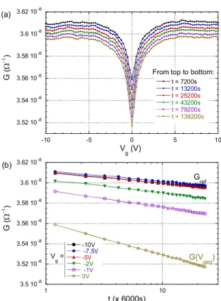
For Fig. 1a, a MOSFET device with a 20nm thick granular Al channel was cooled down to 4.2K and
main-2
FIG. 1: (a) G(Vg) curves measured at different times t after
a cool down to 4.2K. Vg = Vgeq = 0V between Vg sweeps.
(b) Corresponding G(t) curves for negative Vgs in and out of
the conductance dip region. The sample was 20nm thick with R2= 550M Ω at 4.2K. See the text for the details.
tained at this temperature under Vgeq = 0V . Fast Vg sweeps from −15 to +15V (250s long) were taken every 6000s after the cool down. All the G(Vg) curves display a conductance dip centered on Vgeqwhich reflects the mem-ory of the relaxation associated with the stay under Vgeq. Far enough from Vgeq (here for |Vg| > 5V ), G is roughly constant and this baseline reflects the ”off-equilibrium” conductance Gref previously mentioned. Looking at the time evolution of G(Vg) curves, two features are salient. First, the amplitude of the dip increases as a function of time. This result is well known from previous studies [2– 5]: the longer the stay under Vgeq, the more pronounced the dip is. Second, and this is the new feature we aim to discuss here, the baseline conductance also decreases as a function of time. As highlighted in Fig. 1b, the G decrease is well described at any Vgs by a ln t depen-dence, more pronounced in the dip region because of the superposed baseline relaxation and dip growth.
To be more quantitative, we can define a parameter whose physical meaning will become clear later, the slope ratio SR of the G relaxation slope in Fig. 1b at Vgeq to the Gref relaxation slope (at −10V for example). For the sample of Fig. 1, SR ≃ 2.9. We have measured 4
different 20nm thick films with R2values from 10M Ω to 10GΩ. A baseline relaxation was always observed, with SR at 4K between 2 and 3. For one film, the gate and the gate insulator were respectively Al and alumina and consistent results were obtained which excludes any role of a specific gate insulator material. Detailed investiga-tion of the vertical electrical homogeneity of the films has also shown that the baseline relaxation is not related to a specific layer close to the film-substrate interface [10].
We checked that this baseline relaxation was indepen-dent of the Vg history by using the ”two dip” protocol [5]. After some time under Vgeq1, Vgeq was changed to Vgeq2 for the rest of the experiment. We observed the formation of a new dip at Vgeq2 and the erasure of the old one at Vgeq1 (as already known [3, 5]), but the base-line relaxation in any Vgrange far enough from Vgeq1and Vgeq2 continue as if no Vgeq change was imposed.
One may think that the baseline relaxation is induced by the Vg sweeps themselves. Indeed, when measuring G(Vg) curves, a small dip starts to form at each measured point. The baseline thus reflects a short time relaxed G value (10s being typical for our sweep parameters). We know from the ”two dip” protocol results that a dip formed during 10s will be erased roughly in about 100s [2, 3]. In our case, we wait for 6000s between two Vg sweeps, thus no memory of the previous sweep is expected out of the dip region. In one experiment, we checked that the baseline relaxation was unaffected by the suspension of Vg sweeps during 30h.
An experimental artifact that may explain the baseline relaxation is the existence of a T drift after the cool down. Because of the rapid divergence of the films resistance at low T , the observed baseline variations correspond typi-cally to drifts of few mK (≃ 2.5mK for the whole relax-ation observed at 4.2K in Fig. 1). We have performed different tests (thermometer stability, comparison with and without He exchange gas) which indicate that the T drifts are much smaller than the baseline relaxation am-plitude. The effect of the film thickness discussed below will definitely ruled out any interpretation in terms of a T drift.
If the baseline relaxation is a property of the granular film itself, how can we explain it? A simple hypothesis is to state that the granular Al film, although electri-cally insulating, has a metallic-like screening length Lsc that is smaller than its thickness Th (Th= 20nm in Fig. 1). Then, only the layer of the film located at a distance smaller than Lscfrom the gate insulator is sensitive to Vg changes. The conductance dip ∆Gdip reflects the relax-ation of this layer, whereas the conductance baseline Gref reflects the relaxation of the rest of the film. The conduc-tance relaxation measured at Vgeq is then the sum of the two contributions: ∆G(Vgeq, t) = ∆Gdip(t) + ∆Gref(t). Since the relaxations at any Vg are well described by a ln t dependence, we can write ∆Gref(t) = −Arefln t and ∆Gdip(t) = −Adipln t. The slope ratio SR is by
defini-FIG. 2: G(t) measurements after a cool down at 4.2K for: (a) a 10nm thick film, R2 = 6GΩ; (b) a 100nm thick film,
R2 = 2M Ω. The G(t) relaxations are plotted at 0V (Vgeq)
and at −10V (baseline relaxation Gref).
tion equal to (Adip+ Aref)/Aref. If the film is homo-geneous, it is natural to suggest that Adipand Aref are respectively proportional to Lsc (the Vg sensitive layer thickness) and Th− Lsc (the Vg insensitive layer thick-ness). Then, SR = Th/(Th− Lsc) as long as Th > Lsc. The results for the 20nm films (SR between 2 and 3) give estimates for the screening length Lsc between 10 and 13nm.
If our simple model is correct, then the baseline relax-ation relative to that measured at Vgeq must change with the thickness of the films. This is illustrated in Fig. 2, where the experiment of Fig. 1 was reproduced for two granular Al films 10nm and 100nm thick. A clear thick-ness dependence is visible. Qualitatively, the baseline relaxation is almost absent for the 10nm thick film (Fig. 1a, SR = 20) while it is almost equal to that measured at Vgeq for the 100nm thick film (Fig. 1b, SR = 1.1). The agreement with the above simple picture is also quan-titative. These SR values gives Lsc estimates of about 10nm, close to the results obtained from 20nm thick films (10 − 13nm). We stress that the SR variations observed for different thicknesses are much more important than those observed for a given thickness and different R2s.
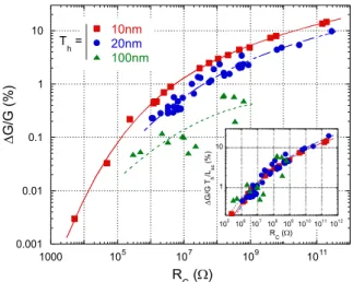
Our simple model also predicts a thickness depen-dence for the amplitude of the conductance dip ∆G/G = [Gref− G(Vgeq)]/Gref. ∆G/G data, measured for 10nm,
20nm and 100nm thick films are shown in Fig. 3 as a function of their percolation critical resistance RC [11]. In 2D films (Th less than the percolation radius L0), RC ≃ R2, but for thicker ones, RC≃ (Th/L0)R2. Tak-ing L0 ≃ 20nm [12], we estimate RC as R2 for 10 and 20nm films and 5R2 for 100nm films. All the sam-ples were measured after being kept under Veq= 0V for t = 20h after a cool down at 4.2K. As can be seen and was already reported [1, 3], ∆G/G increases significantly with RC. Besides, a clear reduction of ∆G/G is visible for a given RC as Th increases, in qualitative agreement with the fact that the conductance dip originates from a layer of a fixed thickness. The agreement is also quanti-tative. As long as Th < Lsc, ∆G/G(t) does not depend on Th. Let us note its value C(t) (of course C(t) de-pends on RC). When Th > Lsc, one has ∆G/G(t) = Adipln t/(G0− Arefln t) ≃ Adipln t/G0 = C(t)Lsc/Th (∆G/G(t) ≪ 1). Then, plotting (Th/Lsc) × (∆G/G) for all the samples should give one single curve C(t, RC). This is confirmed in the inset in Fig. 3 for which we have assumed a screening length of 10nm for all the films.
Finally, our model provides a natural explanation for the increase of the ∆G/G data scatter with the thick-ness, as observed in Fig. 3. Small variations of the O2 pressure or of the Al evaporation rate are always present during the deposition of granular Al films. Thus in thick samples, the measured R2 (and the estimated RC) does not necessarily reflect the resistance of the unscreened 10nm thick layer deposited on top of the gate insulator which determines the amplitude of the dip. The quality of the scaling in the inset in Fig. 3 is indeed an indirect test of the vertical homogeneity of the films, as discussed in details in Ref. [10].
We now come to a discussion of our results. First, note that the thickness dependence of SR clearly demon-strates that the conductance relaxation exists in the ”bulk”” of the film and is a property of the granular Al itself (and not of its interface with the gate or the surface oxide layer). The ”bulk” relaxation after a cool down at 4.2K is well described by a ln t dependence without any sign of saturation over weeks of measurement. Such a ln t dependence was also observed for the time increase of the conductance dip amplitude after a cool down [2, 3] (more complex laws are observed when Vgeq is fixed a time te after the cool down, see [4]). It is a natural relaxation law for a system having a 1/τ distribution of relaxation times, as expected for an electron glass [13].
In our granular Al thin films, the electronic transport at finite T is believed to result from electron tunneling between metallic Al grains. A lower bound for Lsc is then the typical grain size, which was found in recent TEM measurements to be 2 − 4nm. A second impor-tant microscopic length scale is the percolation radius L0 of the critical resistance network. Since in our films RC.100GΩ, the diffusion of charge carriers through the critical resistance network is expected to be faster than
4
FIG. 3: ∆G/G values measured 20h after a cool down at 4.2K as a function of RC(see the text for the details). The films are
10nm (squares), 20nm (circles) and 100nm (triangles) thick. The lines are guides for the eye. In the inset, (∆G/G) × (Th/Lsc) versus RC. Typical error bars on each point are
about 10%.
the time scale of the measurements (the intergrain ca-pacitance and the caca-pacitance of the granular Al channel to the gate are respectively ≃ 10−19F and ≃ 10−11F ). Thus, L0should be an upper bound for Lscas indeed ob-served: L0estimates from conductance fluctuations mea-surements are between 20nm and 40nm [12], a few times our Lscvalue.
We note that no baseline relaxation was reported on 20nm thick indium oxide films which may indicate that Lsc(4K) > 20nm in this system. Interestingly enough, L0 was found to be ≃ 300nm in ”crystalline” films [14], i.e. ≃ 10 times our estimate for granular Al films, re-flecting a less dense percolating network in indium oxide consistent with a larger screening length.
Our observations address the important question of screening in a disordered insulator, a subject which has been little explored both theoretically and experimen-tally. Electron glass models are generally developed in the limit of strongly localized electrons [7–9] (Ref. [15, 16] are exceptions). But in real systems, there is a mobility of the charge carriers at finite T which will give rise to a metallic-like screening. Numerical stud-ies on disordered insulators have indeed found a transi-tion between a metallic screening at high T where most of the electrons are diffusive and a slow dielectric re-sponse at low T where most of the electrons remain lo-cated in finite size clusters [17–19]. Such a transition was observed around 1K in capacitive measurements on a doped semiconductor [20]. According to the usual formula, L2
sc = ǫǫ0/e 2
dN/dµ(EF), where dN/dµ is the thermodynamic DOS. In a glassy phase and for a finite time t, the system cannot explore all the configurations
and the thermodynamic DOS has to be replaced by a pseudo-equilibrium DOS dN/dµ(t) for which only relax-ations faster than t are allowed. The first theoretical attempts to do so [7, 21] have found that the short time (≃ Maxwell time) screening length diverges as T goes to 0 and decreases as a function of time [21].
In summary, we have described in insulating granular Al films the existence of a Vg insensitive conductance relaxation. Its thickness dependence demonstrates the existence of a metallic screening length of about 10nm at 4K. Our results provide a new way to study the screening length and its relaxation in disordered insulators where an anomalous electrical field effect has been found. They also point to the need for more theoretical studies: how are the classical electron glass models predictions affected by the existence of a metallic screening length ?
This research has been partly supported by the French-National Research Agency ANR (contract No05−JC05− 44044).
[1] M. Ben-Chorin et al., Phys. Rev. B 44, 3420 (1991); G. Martinez-Arizala et al., Phys. Rev. Lett. 78, 1130 (1997); T. Grenet, Eur. Phys. J. B 32, 275 (2003).
[2] A. Vaknin et al., Phys. Rev. B 65, 134208 (2002). [3] T. Grenet et al., Eur. Phys. J. B 56, 183 (2007). [4] T. Grenet et al., to be published in Eur. Phys. J. B. [5] A. Vaknin et al., Phys. Rev. Lett. 81, 669 (1998). [6] Z. Ovadyahu, Phys. Rev. Lett. 99, 226603 (2007);
Z. Ovadyahu, Phys. Rev. B 78, 195120 (2008); Z. Ovadyahu, Phys. Rev. Lett. 102, 206601 (2009). [7] J. H. Davies et al., Phys. Rev. Lett. 49, 758 (1982). [8] M. Gr¨unewald et al., J. Phys. C 15, L1153 (1982); M.
Pollak and M. Ortu˜no, Sol. Energy Mater. 8, 81 (1982). [9] For recent Ref., see C.C. Yu, Phys. Rev. Lett. 82, 4074 (1999); D.N. Tsigankov et al., Phys. Rev. B 68 184205 (2003). M. M¨uller and L. Ioffe, Phys. Rev. Lett. 93, 256403 (2004); V. Malik and D. Kumar, Phys. Rev. B 69, 153103 (2004); D.R. Grempel, Europhys. Lett. 66, 854 (2004); E. Lebanon and M. M¨uller, Phys. Rev. B 72, 174202 (2005); A.M. Samoza et al., Phys. Rev. Lett. 101, 056601 (2008).
[10] See EPAPS Document No for a discussion of the vertical
electrical homogeneity of the granular Al films.
[11] B.I. Shklovskii and A.L. Efros, Electronic Properties of Doped Semiconductors (Springer-Verlag, New York 1984).
[12] J. Delahaye et al., Eur. Phys. J. B 65, 5 (2008). The existence of a screening length was not taken into account in this Ref. and the L0 values reported for 20nm films
must be divided by a factor Th/Lsc≃√2.
[13] A. Amir et al., Phys. Rev. B 77, 165207 (2008); A. Amir et al., Phys. Rev. Lett. 103, 126403 (2009).
[14] V. Orlyanchik and Z. Ovadyahu Phys. Rev. B 75, 174205 (2007).
[15] G. Vignale, Phys. Rev. B 36, 8192 (1987).
[16] A.A. Pastor and V. Dobrosavljevi´c, Phys. Rev. Lett. 83, 4642 (1999); V. Dobrosavljevi´c et al., Phys. Rev. Lett. 90, 016402 (2003).
[17] W. Xue and P.A. Lee, Phys. Rev. B 38, 9093 (1988). [18] A.B. Kolton et al., Phys. Rev. B 71, 024206 (2005). [19] A. D´ıaz-S´anchez et al., Phys. Rev. B 59, 910 (1999). [20] Don Monroe et al., Phys. Rev. Lett. 59, 1148 (1987).
[21] M. M¨uller and S. Pankov, Phys. Rev. B 75, 144201 (2007).