HAL Id: hal-00591005
https://hal.archives-ouvertes.fr/hal-00591005
Submitted on 6 May 2011
HAL is a multi-disciplinary open access
archive for the deposit and dissemination of
sci-entific research documents, whether they are
pub-lished or not. The documents may come from
teaching and research institutions in France or
abroad, or from public or private research centers.
L’archive ouverte pluridisciplinaire HAL, est
destinée au dépôt et à la diffusion de documents
scientifiques de niveau recherche, publiés ou non,
émanant des établissements d’enseignement et de
recherche français ou étrangers, des laboratoires
publics ou privés.
An Ultra Small Passive Balun for 60 GHz Applications
in CMOS 65nm Technology
Mariano Ercoli, Michael Kraemer, Daniela Dragomirescu, Robert Plana
To cite this version:
Mariano Ercoli, Michael Kraemer, Daniela Dragomirescu, Robert Plana. An Ultra Small Passive
Balun for 60 GHz Applications in CMOS 65nm Technology. IEEE International NEWCAS Conference
(NEWCAS 2010), Jun 2010, Montreal, Canada. p 329-332. �hal-00591005�
An Ultra Small Passive Balun for 60 GHz
Applications in CMOS 65nm Technology
Mariano Ercoli, Michael Kraemer, Daniela Dragomirescu, Robert Plana
CNRS; LAAS; 7 avenue du colonel Roche, F-31077 Toulouse, France University of Toulouse ; UPS, INSA, INP ISAE; LAAS; F-31077 Toulouse, France
mercoli@laas.fr; mkraemer@laas.fr; daniela@laas.fr; plana@laas.fr
Abstract—In this paper a novel method to design a miniatur-ized Marchand Balun is proposed. The main issue in the balun design is to limit its physical dimension. This work shows a device that achieves good performance, in terms of phase and amplitude balance, and reduced size at the same time. To allow such a result, an accurate analysis of the electromagnetics phenomena was done. The principal equations that characterize the structure are resumed in the paper. The device has been fabricated in 65 nm CMOS technology. The balun has been designed for application in a wide band low power 60 GHz transceiver.
Index Terms—Marchand Balun, Coupled Line, 60GHz Band, CMOS.
I. INTRODUCTION
In the last decade the development of wireless applications has had a rapid growth. This trend has interested especially the 60 GHz unlicensed band that offers a very large applications scenario. The need for cheap, small and at the same time very efficient transceivers has pushed the researcher to find new solution or to improve the actual resources. Moreover the miniaturization of the circuits, due to the scaling of the technology nodes of the transistors, promoted the employment of differential circuits to realize the fundamentals blocks on the transceivers. The balun is a fundamental component for this type of architecture. This device finds wide ap-plication in antennas, push-pull amplifiers, balanced mixers, etc. If necessary such a device can be designed to achieve impedance matching the other blocks [1] [2]. The employment of differential architectures on RF front-end exhibits many attractive characteristics. For the double balanced mixer, the differential circuit configuration increases the RF-to-IF and LO-to-IF isolation [3] and at the same time it maximizes the common mode rejection. On the other side, in the push-pull amplifier configuration its use increases the linearity and power efficiency of the amplifier. The advantages shown are directly correlated to the performances of the balun. If its behaviour is far from ideal, the performance of the entire system fails. The principal features employed to estimate the quality of the balun are the amplitude balance and the phase balance. The balun can be realized in two different manners: active and passive configurations. For our application, we will focus our attention on passive baluns to obtain a low power circuits.
II. MARCHANDBALUNTHEORY
Regarding the Radio Frequency Integrated Circuit (RFIC) design, the principal issue about the use of this component is
its very large occupied area compared with the active circuit parts. In literature, many architectural solutions for the balun design are available, and a large part of those have as objective the reduction of the physical dimension. Table 1 summarizes the state of the art of these devices. The various typologies of baluns taken into account are realized on different tech-nologies (Si, SiGe and GaAs). The interest of this work is focused on the geometrical realization. The different substrate typologies influence the total dimension through the relative permittivity constant (εr), but by an efficient architectural
solution it is possible to achieve the minimum area in all types of substrate. The cost of the chip fabrication increases proportionally with the area, thus the miniaturization of this component is extremely important. The different topologies of passive baluns can be classified in two different categories: Classical Marchand Balun [4, 5], with its derivations, [6, 7, 8, 9, 10] and Conventional transformer [11]. On silicon bulk CMOS technology the effective permittivity constant εef f is
about 4.2 as a consequence the wavelength (λ) at 60 GHz is 2.6 mm, so λ/4 = 650 µm. To avoid this large waste of area, literature proposes different solutions: spiral approach [6] or meandered displacement [5, 16]. However the problem is not completely solved since the dimension of the structure is still too big. In this work the different solutions shown in Table 1 have been analised to understand which possible architecture can be employed to further improve its response. The operating principle for the proposed balun is based on the classical Marchand balun design [18]. The difference between the classical and the proposed structure is the dimension of the coupled lines that form the balun. The Marchand balun architecture is realized by a pair of coupled lines with a λ/4 length. In this new solution the lines’s length have been reduced. To achieve a response comparable with the one of the Marchand balun it has been necessary to understand the physics phenomena of the structure. The analysis started by a pair of general equation that model the Marchand Balun [6]:
S21,bal= −T C + T3C 1 + C2 (1) S31,bal= T C − T3C 1 + C2 = −S21 (2)
Where T and C represent respectively the transmitted and the coupled power into the balun (bal). To understand the
TABLE I
STATE OF THE ART FOR MILLIMETER-WAVEBALUNS(*SIMULATED VALUES)
Bandwidth [GHz] Insertion Loss [dB]
Input Return Loss [dB] Amplitude Imbalance [dB] Phase Imbalance[Deg] Occupied Area [mm2]
This Work 50-70 1.1* <14* <0.1* Max 5 0.01
[5] 25-65 <10 <10* 1.5 < ±10 0.55 [8] 14-28 <1.5 <15 1 < ±10 0.26 [10] 20-26 <2 N.A. 0.5 Max 5 0.05 [11] 50-65 3 N.A. <3 Max 5 0.05 [12] 20-70 1 N.A. 1 5 0.06 [13] 15-45 1.5 <13 1 5.5 0.40 [14] 18-32 0.8 <12 1 5 0.07 [15] 27-54 1.1 <15 <1 5 0.06
functioning of the balun is necessary to know the distribution of principal power flows of the structure.
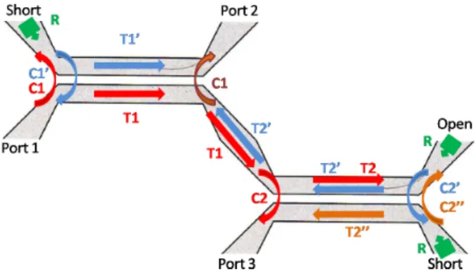
Equations (1) and (2) summarize the different contributions that came out at the balanced ports but do not show which is the importance of each coefficient. This can be explained using Figure 1, which shows the propagation of power into the structure at different time steps. The values of the coupling and transmission factor into the two couplers must be chosen carefully. For example, a too high value for the C1 factor is counter-productive because the power reflected by the short R is reflected back to the input. The same problem occurs for a too low value of C1: in this condition the power transmitted on Port 2 is too low. For the project described in this paper the
Fig. 1. Balun with its principal power flows
coupled lines theory [17] is employed to model the couplers that constitute the balun. The model of the coupled lines is based on the field mode analysis. It is known that two different modes exist on the coupled structure: the even and odd modes. The superposition of those two groups of modes influences the coupler behaviour and therefore the balun response. Equation (3) describes the influence that the two modes have on the output imbalance [5]. S21,bal S31,bal =Z0e− Z0o Z0e+ Z0o (3) The coefficients Z0e,o are impedances of the even and odd
modes respectively. Z0e= r L + M C (4) Z0o= r L − M C + 2Cm (5) For the single coupled line, equation (3) can be used to characterize the coupling factor:
C = Z0e− Z0o Z0e+ Z0o
(6) In the silicon bulk technology limits exist for the maximum value for the even mode impedance. Its value is limited by the parasitic capacitance between the lines and the ground [13]. A reasonable value for this parameter is around 100 to 150 Ohm [16]. Such a limit for the maximum even impedance moves the attention to the optimization of the other parameters: the mutual capacitance Cmand the mutual inductance M between
the coupled lines become fundamental design variables (5). Moreover the even and odd mode impedances are important in terms of matching impedance among the balun and the other devices. For the coupled line model, a relation holds [17] for the even and odd mode impedances to achieve a low return loss:
Z0e∗ Z0o= Zo2 (7)
where Z2
o is the characteristics line impedance. To take into
account the dimension of the coupler’s line a set of equations are well explained in [17]. The principal equations, employed to show the power propagation are:
S12= √ 1 − C2 √ 1 − C2cos θ + j sin θ (8) S13= jC sin θ √ 1 − C2cos θ + j sin θ (9)
In those equations the S parameters are referred to a single coupler device. Therefore they can be employed to model the parameters shown in the (1,2):
S21,bal= − jC1 sin θ T 12cos θ + j sin θ T 1 T 1 cos θ + j sin θ + ... (10) S13,bal= T 1 T 1 cos θ + j sin θ jC sin θ T 2 cos θ + j sin θ − ... (11) where T = √1 − C2. The extended formula was stopped
at fist step of approximation to show the complexity of the calculus. Moreover, in the case of which the electrical length of the two couplers are different there will be two different values of θ , which add further complexity to the problem.
III. LAYOUTREALIZATION
Taking into account the consideration exposed in the Section II the design of balun is started. To minimize the occupied area the branches of the coupled lines have been rolled up like an inductor. Moreover the lines that constitute each coupler have been placed on two different metal layers, more precisely on metal 7 for the input lines (green in the Figure 2) and metal 6 for the coupled lines (cyan). This solution guarantees the increase of the mutual magnetic coupling and the mutual capacitance is achieved by stacking the lines. Employing two identical couplers to build the structure, the simulations show a power imbalance of 1.5 dB and around 6 degrees of phase imbalance. This result is expected because the boundary condition for the two coupler are more different (see Figure 1). To reduce the imbalance and perform the input reflection loss, a session of optimization has been set up. The variables chosen for optimization are the physical dimension of the lines that constitute the device. Figure 2 shows the group of optimized variables. The black arrows represent the dimension
Fig. 2. Layout of Balun.
of secondary coupled lines, the red ones instead are referred to the input lines. W is the line width, D is the vertical and horizontal diameter of the coils, P is the pitch between the lines, C is the coils distance. The variables A and G model the free ground area around the structure and the ground contact respectively. The ground layer has a strong influence for the balun response. There are two reasons: the first, concerns the confining of the magnetic field around the coils and the second one, concerns the role of ground contact for the output coupled coils. The sizing of the ground contact is a trade off between the parasitic coupling with the lines (that cause a drop off of impedance for the even mode) and the parasitics inductance generated on the metal contact. This inductance value, estimated around at 10-15 pH for a worst case, has a very strong effect on the balun in terms of power imbalance. Simulations show a maximum imbalance of 0.4 dB for a wrong design of the contact. To reduce the parasitics inductance, A1 must be high. In this condition the inductance effect is
attenuated and the imbalance removed. The only constraint to assure the same impedance on the balanced output is on the values of the width of the secondary coils: W1,2= W2,2.
For the other parameters the only limit imposed is the respect of the design kit dimension rules. After the optimization run the dimensions of the two coils structures are very different. Figure 3 shows a 3D representation of the structure.
Fig. 3. Balun layout after the cycle of optimization.
IV. SIMULATIONRESULTS
The optimization run and the simulation were performed using Sonnet Release 12, version 12.52. This approach, for the design of miniaturized passive structures, has been widely employed and confirmed by measurements in a previous work [19]. The balun response demonstrates the effectiveness of the design flow. Figure 4 shows the transmission power in terms of S21 and S31 and the reflection loss S11 The power
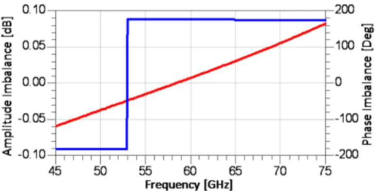
dissipation for the balun after the 3 dB subtraction due to the power split is 1.12 dB at 60 GHz. Regarding the peak of the reflection coefficient, it is possible to observe that it is not placed in the middle of the band of interest. This is due to the trade off among the minimization of power imbalance, (see equation (3)), and the input matching condition, (see equation (7)). However, the value of reflection coefficient is lower than 13 dB within the whole band of interest. On Figure 5 is shown the power and phase difference of the balanced output. The power imbalance for the structure is very limited with a maximum gap of 0.1 dB. Regarding the phase imbalance there is a topology constraint that imposes a limit to the minimum phase imbalance. The constraint is represented by the tapered
Fig. 4. Output balun response and input return loss
Fig. 5. Power and phase imbalance between the differential output ports
the phase shift in the second coupler. The phase gap can be reduced by a reduction of coupled lines length, but this action would degrade the power balance degrade. The best trade off is reached with 5 degree of imbalance: a large band response for the balun in this case is shown in Figure 6.
Fig. 6. Wide band response of the balun
The imbalance for the power and the phase increases for the higher frequencies but it remains limited to 0.4 dB and 8 degree at 90 GHz. At frequencies below 40 GHz the balun response drops down. This behaviour can be explained considering equations (10) and (11). The coupling to the balanced output depends on the electrical length of the line. For the frequency below 40 GHz θ is too short to guarantee a sufficient coupling. The power remains on the primary lines until the open circuit point, where the open line reflects the signal to unbalanced port (Port 1). The real dimension for the lines length employed to build the balun are about λ/12. This very low value for the length becomes too short for the low frequencies. The behaviour of the S11 parameter for low
frequency confirms this explanation. V. CONCLUSION
This paper shows a new method to synthesize a balun for the RFIC design. The size, including of the ground free area is 127×79 µm, which is, to our knowledge, the smallest structure of this kind demonstrated so far. The balun simulations show a very flat response, for the whole operating band (57 - 63 GHz) and the device can also be employed to higher frequencies
without severe performance degradation. The balun decreases its performance for very high frequencies but the S11 remains however lower than -10 dB until 90 GHz. The low input return loss assures a good matching for the 50 Ohm source. The balun will be employed in a 60 GHz up-converter mixer. The fabrication run is scheduled for March 2010, using the CMP facilities (http://cmp.imag.fr/).
REFERENCES
[1] Kidwai, A.A. and Nazimov, A. and Eilat, Y. and Degani, O., Fully integrated 23dBm transmit chain with on-chip power amplifier and balun for 802.11a application in standard 45nm CMOS process, 3rd Radio Frequency Integrated Circuits Symposium, 2009. RFIC 2009. IEEE , 2009.
[2] Van Vorst, D. and Mirabbasi, S., Low-power 1V 5.8 GHz bulk-driven mixer with on-chip balun in 0.18m CMOS, Radio Frequency Integrated Circuits Symposium, 2008. RFIC 2008. IEEE , 2008.
[3] Komoni, K. and Sonkusale, S., Modeling, simulation and implementation of a passive mixer in 130nm CMOS technology and scaling issues for future technologies, Circuits and Systems, 2008. MWSCAS 2008. 51st Midwest Symposium on. IEEE , 2008.
[4] Ng, C.Y. and Chongcheawchamnan, M. and Robertson, I.D., Analysis and design of a high-performance planar Marchand balun, Microwave Symposium Digest, 2002 IEEE MTT-S International IEEE , 2002. [5] Liu, J.-X. and Hsu, C.-Y. and Chuang, H.-R. and Chen, C.-Y., A 60-GHz
Millimeter-wave CMOS Marchand Balun, Radio Frequency Integrated Circuits (RFIC) Symposium, 2007 IEEE , 2007.
[6] Ang, K.S. and Economides, S.B. and Nam, S. and Robertson, I.D., A compact MMIC balun using spiral transformers, Microwave Conference, 1999 Asia Pacific IEEE , 1999.
[7] Zhen-Yu Zhang and Yong-Xin Guo and Ong, L.C. and Chia, M.Y.W., A new planar Marchand balun, Microwave Symposium Digest, 2005 IEEE MTT-S International IEEE , 2005.
[8] Sun, Q. and Yuan, J. and Vo, V. T. and Rezazadeh, A. A., Design and Realization of Spiral Marchand Balun Using CPW Multilayer GaAs Technology, Microwave Conference, 2006. 36th European IEEE , 2006. [9] Tzyh-Ghuang Ma and Yu-Ting Cheng, A Miniaturized Multilayered Marchand Balun Using Coupled Artificial Transmission Lines, Microwave and Wireless Components Letters IEEE , 2009.
[10] Lai, I.C.H. and Fujishima, M., An Integrated 20-26 GHz CMOS Up-Conversion Mixer with Low Power Consumption, Solid-State Circuits Conference, 2006. ESSCIRC 2006. Proceedings of the 32nd European IEEE , 2006.
[11] Felic, G. and Skafidas, E., An Integrated Transformer Balun for 60 GHz Silicon RF IC Design, Signals, Systems and Electronics, 2007. ISSSE ’07. International Symposium on IEEE , 2007.
[12] Van Vorst, D. and Mirabbasi, S, Low-power 1V 5.8 GHz bulk-driven mixer with on-chip balun in 0.18m CMOS, Radio Frequency Integrated Circuits Symposium, 2008. RFIC 2008. IEEE , 2008.
[13] Hamed, K.W. and Freundorfer, A.P. and Antar, Y.M.M., A monolithic double-balanced direct conversion mixer with an integrated wideband passive balun, Solid-State Circuits, IEEE Journal of. IEEE , 2005. [14] H.-Y. Yu, S.-S. Choi, S.-H. Kim and Y.-H. Kim, K-band balun with
slot pattern ground for wide operation using 0.18 m CMOS technology, Electronics Letters. IEEE , 2007.
[15] Hwann-Kaeo Chiou and Tsung-Yu Yang, Low-Loss and Broadband Asymmetric Broadside-Coupled Balun for Mixer Design in 0.18- µm CMOS Technology, Microwave Theory and Techniques, IEEE Transac-tions on. IEEE , 2008.
[16] Chun-Hsien Lien and alt., Analysis and Design of Reduced-Size Marc-hand Rat-Race Hybrid for Millimeter-Wave Compact Balanced Mixers in 130-nm CMOS Process, Microwave Theory and Techniques, IEEE Transactions on. IEEE , 2009.
[17] R. Sorrentino, G. Bianchi, Ingegneria delle microonde e radiofrequenze, Mc Graw Hill , 2007.
[18] N. Marchand, Transmission-line conversion transformer, Electron., vol. 17, no. 12, pp. 142145 , 1944.
[19] M. Kraemer, D. Dragomirescu, and R. Plana, Accurate electromagnetic simulation and measurement of millimeter-wave inductors in bulk CMOS technology,10th Topical Meeting on Silicon Monolithic Integrated Cir-cuits in RF Sistem, January 2010.