HAL Id: hal-02135849
https://hal.archives-ouvertes.fr/hal-02135849
Submitted on 12 Jun 2019HAL is a multi-disciplinary open access archive for the deposit and dissemination of sci-entific research documents, whether they are pub-lished or not. The documents may come from teaching and research institutions in France or abroad, or from public or private research centers.
L’archive ouverte pluridisciplinaire HAL, est destinée au dépôt et à la diffusion de documents scientifiques de niveau recherche, publiés ou non, émanant des établissements d’enseignement et de recherche français ou étrangers, des laboratoires publics ou privés.
Free-standing La 0.7 Sr 0.3 MnO 3 suspended
micro-bridges on buffered silicon substrates showing
undegraded low frequency noise properties
S Liu, B. Guillet, C. Adamo, V Nascimento, S Lebargy, G Brasse, F Lemarié,
J El Fallah, D.G. Schlom, Laurence Méchin
To cite this version:
S Liu, B. Guillet, C. Adamo, V Nascimento, S Lebargy, et al.. Free-standing La 0.7 Sr 0.3 MnO 3 suspended micro-bridges on buffered silicon substrates showing undegraded low frequency noise properties. Journal of Micromechanics and Microengineering, IOP Publishing, 2019, 29 (6), pp.065008. �10.1088/1361-6439/ab16ac�. �hal-02135849�
1
Free-standing La0.7Sr0.3MnO3 suspended micro-bridges on buffered silicon substrates
showing undegraded low frequency noise properties
S. Liu1, B. Guillet1, C. Adamo2,3, V. M. Nascimento1, S. Lebargy1, G. Brasse4, F. Lemarie4, J. El Fallah5, D.G. Schlom2,6, L. Méchin1
1
Normandie Univ, UNICAEN, ENSICAEN, CNRS, GREYC, 14000 Caen, France 2
Department of Materials Science and Engineering, Cornell University, Ithaca, New York 14853-1501, USA
3
Department of Applied Physics, Stanford University, Stanford, CA 94305, USA 4
Normandie Univ, ENSICAEN, UNICAEN, CEA, CNRS, CIMAP, 14000 Caen, France 5
Normandie Univ, ENSICAEN, UNICAEN, CNRS, LCS, 14000 Caen, France 6
Kavli Institute at Cornell for Nanoscale Science, Cornell University, Ithaca, New York 14853-1501, USA
Corresponding author : laurence.mechin@ensicaen.fr
Keywords: functional oxides, MEMS, low frequency noise, fabrication process
Abstract
We report on the microfabrication process of free-standing suspended micro-bridges made of La0.7Sr0.3MnO3 (LSMO) thin films of thicknesses in the 10 – 100 nm range. LSMO films were epitaxially grown on either SrTiO3 or CaTiO3 buffer layers on silicon substrates by reactive molecular beam epitaxy. The micro-bridges were patterned using standard UV photolithography then etched by ion beam and released using reactive ion etching of silicon in SF6. 2 and 4 µm wide LSMO suspended micro-bridges of length ranging from 50 to 200 µm could be fabricated with a high fabrication yield (of about 85% as evaluated over 100 fabricated suspended micro-bridges) without degrading the electrical transport properties and in particular the low frequency noise level, as attested by the normalized Hooge parameter. The latter was measured in the 0.55 – 7.50 ×10⁻³⁰ m3 range at 300 K, which is comparable to those measured in non-suspended high quality epitaxial LSMO thin films. This fabrication process could be useful for bolometer fabrication where thermal isolation is needed, or for any MicroElectroMechanical Systems devices making use of epitaxial functional oxides.
2
1- Introduction
The manganite composition La0.7Sr0.3MnO3 (LSMO) is an example of promising material for a new generation of devices and sensors operated at room temperature including thermal sensors, spintronic devices, magnetic or pressure sensors [1-5]. LSMO belongs to the class of transition-metal oxides, characterized by unprecedented functionalities, often being relevant to different fields of application [6-9]. However unsolved technological fabrication issues still exist before these materials could be used in real applications. In particular, the epitaxial growth, necessary to achieve optimal properties of these complex materials in the form of thin films, induces high residual strain that is detrimental to fabrication reliability, and imposes the use of ceramic substrates with well lattice matched parameters and deposition of at high temperature. The last two conditions often make fabrication processes using oxide epitaxial films not compatible with the most commonly used fabrication processes based on silicon, such as the micromachining techniques used for MicroElectroMechanical Systems (MEMS) on silicon substrates [10,11].
Silicon substrates are not well adapted to the epitaxial growth of oxides due to the presence of an amorphous SiO2 layer at the Si surface, to the interdiffusion of oxide with Si at the high temperature needed for growing epitaxial oxide films, and finally due to the large difference in the thermal expansion coefficients between oxides and Si. These problems can be overcome by introducing single or multiple buffer layersas seenin literature [12-21] and our previous work [22-25], but the residual stress in the high quality epitaxial thin films are high thus making the fabrication of suspended structures challenging. Literature data and books describing fabrication techniques and complete processes for silicon-based MEMS are numerous, but reported technological processes for the fabrication of MEMS using epitaxial oxide films are few in literature although it is essential since all aspects from device design, material properties and microfabrication are closely interconnected to achieve the best performance. Using non silicon substrates and chemical etching, several realisations of free-standing structures made of various epitaxial functional oxides [26,27,28,29] and of epitaxial LSMO [30,31] could be achieved. D. Isarakorn et al. reported the microfabrication of piezoelectric MEMS structures based on epitaxial Pb(Zr0.2Ti0.8)O3 (PZT) thin films grown on silicon wafers [32,33]. Silicon membrane or cantilevers were fabricated by backside etching by Reactive Ion Etching (RIE). SrRuO3/PZT/SrRuO3 thin-film stacks have been used by Nguyen et al. to fabricate piezoelectric cantilever arrays with beam lengths ranging from 100 to 800 µm and widths ranging from 50 to 150 µm [34]. The release etching for forming cantilevers was performed by DRIE using a mixture of SF6, O2 and C4F8 gases. Baek et al.
3
showed that high-quality Pb(Mg1/3Nb2/3)O3-PbTiO3 (PMN-PT) epitaxial thin films can be incorporated into silicon microcantilevers that exhibit very large electromechanical coupling for ultrasound medical imaging, microfluidic control, mechanical sensing, and energy harvesting [35]. Silicon-On-Insulator (SOI) substrates can also be used as was done with epitaxial BaTiO3/SrRuO3/YSZ films deposited on Si cantilevers by Colder et al.[36] or with YBa2Cu3O7-(YBCO)/CeO2/YSZ films deposited on suspended Si micro-bridges by Méchin et al.[37]. Kim et al. could fabricate free standing membranes from La 1-x(Sr,Ca)xMnO3/Bi4Ti3O12/CeO2/YSZ on Si wafer using argon etching and inductively coupled SF6 and C4F8 plasma-etching processes [38]. Chromic et al. grew LSMO thin films by pulsed laser deposition (PLD) on Bi4Ti3O12/CeO2/YSZ buffered SOI substrates, and showed tentative experiments where the substrate has been removed from the back side to reduce thermal losses [39].
Our objective is to achieve an optimized reliable and simple microfabrication process of suspended micro-bridges using epitaxial LSMO thin films deposited on buffered silicon substrates for uncooled bolometers. A figure of merit that is commonly used to characterize radiation sensor performance is the Noise-Equivalent Power (NEP). It is defined as the ratio of the noise spectral density Sn (expressed in V·Hz-1/2 or A·Hz-1/2) over the bolometer responsivity (expressed in V·W-1 or A·W-1). Large responsivity is obtained if (i) materials with large temperature coefficient of resistance (TCR), defined as (1/R)×(dR/dT) where R is the electrical resistance and T the bolometer temperature, and (ii) geometries achieving thermal insulation of the active area are used [40-44]. LSMO is a competitive material compared to existing technologies using amorphous silicon [45] or VO2 [46] since it presents a TCR of 0.02 K-1 at room temperature thanks to the large electrical resistance change at the Metal-to-Insulator (M-I) transition [47], and can show very low electrical noise [48,49]. In order to achieve low NEP of the fabricated devices, it should be checked that the fabrication process neither lowers the TCR values nor increases the low frequency noise levels. In this context, section 2 gives the experimental details, including fabrication steps as well as electrical resistance and low frequency noise set-ups. In sections 3, we present electrical resistance versus temperature and low frequency noise measurements in the suspended LSMO bridges. It is shown that a high fabrication yield could be obtained without degrading the electrical transport properties and in particular the low frequency noise level. Finally, a conclusion is given in section 4.
4
2. Experimental
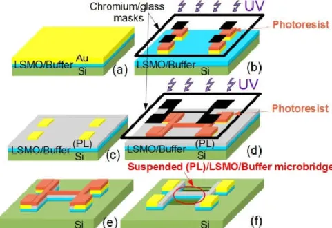
The full fabrication process of our free-standing LSMO suspended micro-bridges is shown in Figure 1. The epitaxial growth of the LSMO/Buffer layers was first achieved on Si (001) substrates by reactive molecular beam-epitaxy (MBE). LSMO thin films with thicknesses ranging from 10 to 100 nm were grown on 20 nm thick SrTiO3 (STO), or CaTiO3 (CTO) buffer layers on Si (001) substrates. Optimized deposition conditions were used in order to obtain high quality epitaxial LSMO thin films as described in previous papers [24,25]. A 200 nm thick gold layer was first deposited on the LSMO/Buffer layers in optimized conditions as described in the next paragraph (figure 1-a) and etched in a potassium iodide solution (Figure 1-b). After gold etching, 20-30 nm thick STO layers were eventually grown by PLD at room temperature on top of the LSMO layers. They served as an additional Protecting Layer (PL) in order to strengthen the suspended micro-bridges in the case of thin LSMO layers (Figure 1-c). Figure 1-d shows the second UV photolithography step for microbridge definition, which was followed by Ar ion beam milling of the (PL)/LSMO/buffer layers down to the silicon substrate as shown in Figure 1-e. Samples were introduced in the Reactive Ion Etching (RIE) chamber and RIE of Si in SF6 gas was finally performed in optimized conditions for isotropic etching (0.05 Torr; 30 sccm; 20 W) from the front side until the micro-bridges are suspended (Figure 1-f) [50].
Figure 1: Fabrication process steps for the fabrication of the LSMO suspended bridges; (a) Deposition of a gold layer on the LSMO/Buffer layers; (b) Contact definition by photolithography and etching of the gold layer; (c) Deposition of an additional Protecting Layer (PL) when necessary; (d) Photolithography of the (PL)/LSMO/Buffer microbridges; (e) Ion beam etching of the (PL)/LSMO/Buffer microbridges down to Si; (f) RIE of silicon.
5
Figure 2: (I-V) characteristics of 15 nm thick LSMO thin films measured at 300 K in a four-probe configuration with four gold contacts deposited in different conditions at 300K and etched in a potassium iodide solution.
Achieving low resistive ohmic contacts on LSMO is quite challenging and has to be carefully optimized before considering any use of LSMO thin films in devices [51]. Electrical contacts must not only be ohmic and low resistive but they have to adhere to the LSMO surface without damaging its properties. The 3 conditions can be contradictory since adhesion is usually reinforced when using energetic deposition methods, which are supposed to be more damaging. During the optimization procedure, we used either Pulsed Laser Deposition (PLD) at room temperature in vacuum or Ion Beam Deposition (IBD) with ion gun at maximum voltage bias (10 keV) or at half of its value (5 keV), or a combination of them to deposit the gold layers on 15 nm thick LSMO layers deposited on STO/Si. Figure 2 shows the current-voltage (I-V) characteristics of different LSMO layers measured in a four probe configuration after the gold layers were defined by standard UV photolithography and etched in a potassium iodide solution. This configuration removes the contribution of the contact resistances. Measurements were made at room temperature in air using a semiconductor parametric analyser (HP-4146B). Firstly, it shows that 200 nm thick Au layer deposited by IBD at 10 keV results in non ohmic contacts, and high electrical resistivity of the LSMO layer. Reducing the gun voltage to 5 keV during Au deposition lead to ohmic contacts but the electrical resistivity of the LSMO layer was around 10 m∙cm at 300 K, which is higher than expected [33]. In order to overcome this problem we deposited Au on LSMO by PLD at room
6
temperature and in vacuum (10-6 mbar). The electrical resistivity of the LSMO layer was still of a higher value than expected for this LSMO composition. Finally, the combination of about 40 nm thick Au layer deposited by PLD and about 160 nm thick Au layer deposited by IBD at 10 keV was chosen. This method does not degrade the LSMO layer resistivity as it was 1.3 m∙cm, which is very close to that of as-deposited LSMO films. The gold layers thus deposited showed good adhesion and good reproducible quality.
We used a prober in a four probe configuration with a variable temperature stage (LAKESHORE TTP4) to heat the sample from room temperature up to around 360 K in a primary vacuum atmosphere. A semiconductor parametric analyser (HP-4146B) was used to plot the current-versus-voltage (I–V) characteristics. The electrical resistivity values were deduced from the slope of I–V characteristics at low current values after having checked the linear nature of the curves (i.e., the ohmic behavior). A low noise high output impedance DC current source and a dedicated low noise instrumentation amplifier with a voltage gain of about 1000, a 1 Hz–100 kHz bandwidth, an input voltage white noise of 20 × 10-18 V2·Hz-1, and negligible input current noise, were used for the low frequency noise measurements. A spectrum analyzer (HP-3562A) calculates the noise spectral density for frequencies in the 1 Hz–100 kHz range. In order to estimate the voltage noise spectral density of the material, the noise of the electronic readout and the noise of the voltage contacts were removed by subtracting the noise spectral density measured at zero bias named SV(0).
3. Results and discussion
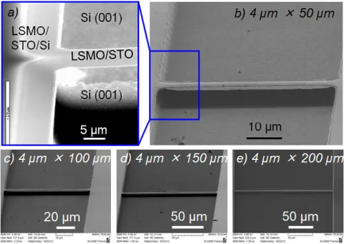
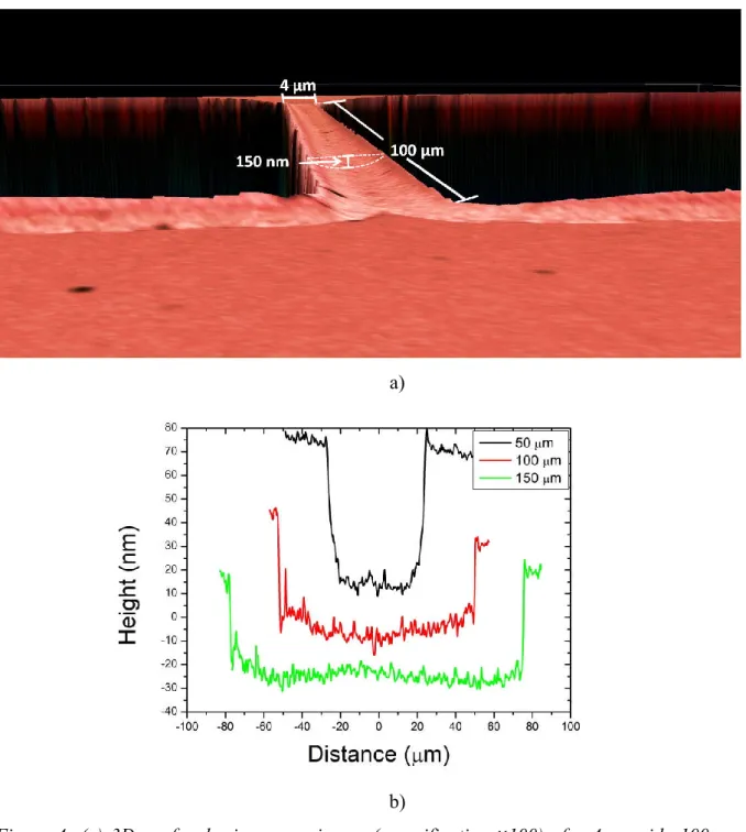
We could successfully fabricate 2 and 4 µm wide free standing (PL)/LSMO/buffer suspended micro-bridges of length 50, 100, 150 or 200 µm (buffer layer being either STO or CTO), using LSMO films in the 10-100 nm range. Typical Scanning Electron Microscope (SEM) photographs are shown in Figure 3. A close view is reported in figure 3-a) where the lateral under etching leaving the LSMO/buffer layers suspended and the remaining Si can be seen. A 3D confocal microscope was used in order to measure the bending of some of the fabricated suspended bridges. An example of the measured images is shown in figure 4-a) for a 4 µm wide 100 µm long suspended bridge patterned in a 75 nm thick LSMO film deposited on STO/Si. Note that the region below the suspended microbridges cannot be reconstructed. A small bending across the width of the microbridges could be observed. It is about 150 nm as measured in the example of figure 4-a). Along the bridges, the deflection is important at the anchor points (as shown in the section profile lines in figure 4-b).
7
Figure 3: Scanning electron microscope (SEM) photographs of free standing 50 nm thick LSMO/CTO suspended micro-bridges. a) Close view of the suspended layers at one side of a suspended micro-bridge. SEM photographs in b) - e) show 4 µm wide 50, 100, 150 and 200 µm long suspended LSMO micro-bridges, respectively.
8 a)
b)
Figure 4: (a) 3D confocal microscope image (magnification ×100) of a 4µm wide 100 µm long suspended bridge patterned in a 75 nm thick LSMO film deposited on STO/Si; (b) Section profile lines along the length (measured at the center of the bridge width) of 50, 100, and 150 µm long LSMO bridges.
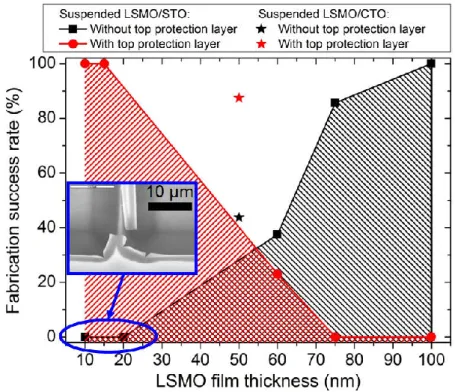
The fabrication success rate of the suspended micro-bridges is reported in Figure 5 as a function of LSMO film thickness for both STO or CTO buffer layers. It was evaluated over about 100 fabricated suspended micro-bridges. For LSMO film thickness below 50 nm the rate is zero when no protecting layer was added. A Scanning Electron Microscope (SEM) photograph is shown in inset of Figure 5 as a typical example of broken structures when using
9
thin LSMO layers. All the observed micro-bridges fabricated in thin LSMO films broke at the joint of the micro-bridges. Because the LSMO/buffer layers are epitaxially grown, residual strain can be sufficiently large to break the bridges when the Si substrate is removed indeed. When a protecting layer was deposited on LSMO films, the success rate increased to 100% for the thinnest LSMO films (10 nm or 15 nm), and to 90% for the 50 nm thick LSMO/CTO micro-bridges (compared to 45% without any protecting layer). It has to be noted that for LSMO film thickness above 60 nm grown using a STO buffer layer, the addition of a protecting layer had bad consequences since the fabrication success rate decreased compared to the value obtained without protecting layer. No evaluation of the mechanical properties was made within this study, and we can only suspect that above a critical total thickness the weight is too large and causes the bridges to break. Considering the best cases (with PL for LSMO thickness below 50 nm and no PL for LSMO thickness above 60 nm) a satisfactory fabrication success rate of about 85 % in average was achieved.
Figure 5: Fabrication success rate of the suspended LSMO bridges versus LSMO film thickness without and with top protection layers (PL). Inset shows a SEM photograph with an example of broken bridge as observed when 10 nm thick LSMO films were used without protecting layers.
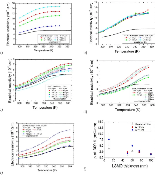
Figure 6 (a-e) shows the electrical resistivity versus temperature characteristics of all the fabricated suspended LSMO micro-bridges. The characteristics of unpatterned as-grown LSMO films are also reported in each graph for comparison, and the electrical resistivity values at 300 K are reported in table 1, together with the maximum TCR values. All the
10
suspended micro-bridges showed a metallic behaviour in the investigated temperature range and a slight increase of the electrical resistivity at 300 K compared to unpatterned LSMO films. It can be observed that the dispersion in the measured electrical resistivity is larger in the suspended bridges fabricated in the 10 nm thick LSMO films, than for thicker films. We believe that this could be simply related to the fact that the same variation of LSMO film thickness all over the substrate surface has more effect on 10 nm than on 100 nm thick LSMO films. No systematic study was made in order to correlate this observation to residual stress that could be present in the suspended structures. Figure 6-f) shows the ratio of the electrical resistivity of suspended micro-bridges over those of unpatterned LSMO films. The ratio is 2 for the 10 nm thick LSMO film and can be as low as 1.2 for thicker LSMO films (75 nm and 100 nm thick) even for 2 µm wide suspended micro-bridges. In the 50-60 nm LSMO thickness range, the electrical resistivity of suspended micro-bridges was increased, about 1.8 times the electrical resistivity of unpatterned films, when STO buffer layers have been used. With CTO the ratio is 1.1 to 1.5 times higher in average than in the unpatterned film. TCR values of LSMO suspended micro-bridges were of the same order in average than those measured in the unpatterned films. All the reported data confirms that our fabrication process did not degrade the DC electrical properties of LSMO suspended micro-bridges for LSMO film thickness above 50-60 nm. CTO buffer layer is interesting since the LSMO electrical resistivity and the phase transition temperature are similar to those LSMO on STO (001) substrates. In the case of 10 to 60 nm thick LSMO/STO suspended micro-bridges, the electrical resistivity was increased by a factor 2 only, which is still sufficiently low to be used in sensor applications.
11
a) b)
c)
d)
e) f)
Figure 6: Electrical resistivity versus temperature characteristics measured in the free-standing LSMO micro-bridges of length L and in the unpatterned films for comparison. a) 4 µm wide 10 nm thick LSMO/STO with PL; b) 4 µm wide 60 nm thick LSMO/STO with PL; c) 2 µm and 4 µm wide 75 nm thick LSMO/STO; d) 2 µm and 4 µm wide 100 nm thick LSMO; e) 2 µm and 4 µm wide 50 nm thick LSMO/CTO with PL; f) Electrical resistivity at 300K of suspended micro-bridges and of unpatterned LSMO films versus LSMO film thickness.
12
Table 1: Electrical resistivity, normalized Hooge parameter (H/n) at 300 K, and maximum of
the TCR values (TCRmax), measured in the unpatterned LSMO films and in the free standing
LSMO suspended micro-bridges.
LSMO thickness (nm) Buffer layer Electrical resistivity at 300 K (×10-5 ·m) TCR max (% K-1) H/n at 300 K (×10-30 m3) As-grown films [24,25] Suspended bridges As-grown films [24,25] Suspended bridges Non suspended strips [24,25] Suspended bridges W=2 µm W=4 µm 10 STO 3.8 - 7.7±2.4 1.6 1.83±0.04 3.41±0.71 7.50±0.40 60 STO 2.8 - 5.0±0.4 2.3 2.61±0.04 0.95±0.25 - 75 STO 2.4 2.5±0.6 2.9±0.3 2.3 2.07±0.10 1.73±0.48 0.95±0.03 100 STO 1.4 1.6±0.6 1.5±0.7 2.1 2.54±0.01 2.75±0.58 0.74±0.05 50 CTO 1.7 2.4±1.4 1.8±0.9 2.5 2.25±0.05 0.42±0.05 0.55±0.03
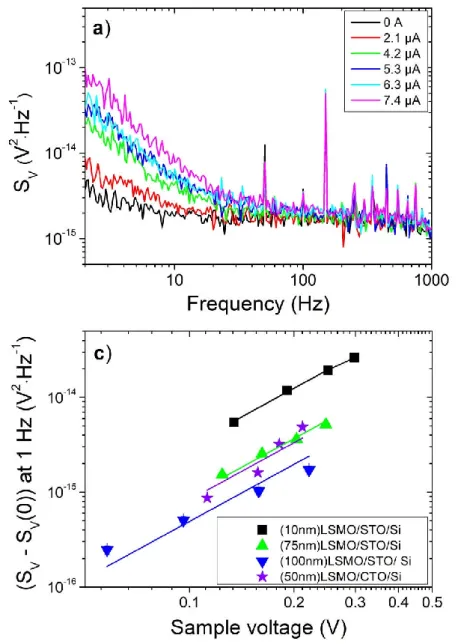
Figure 7 (a-b) present typical voltage noise spectral density spectra measured in the LSMO suspended micro-bridges. We can clearly observe both Johnson (or thermal) noise at high frequency, and 1/f (or flicker) noise at low frequency. In contrast to Johnson noise, which depends neither on bias current nor frequency, the latter gives a frequency and bias current dependent contribution to noise. This type of noise, named l/f since its spectral density is inversely proportional to the frequency, manifests itself as fluctuations in electrical conductance at low frequencies. It is a very fine experimental indicator of the material quality [52] and is usually described by the Hooge empirical relation [53]:
f 1 n V S H 2 V (1)
where SV is the voltage noise spectral density (V2·Hz-1), V is the sample voltage (V), is the Hooge parameter (dimensionless), n is the charge carrier density (m-3), is the sample volume (m3), and f is the measuring frequency (Hz).The normalized Hooge parameter H/n (m3) is very useful to compare the 1/f noise magnitude in different materials independently of the sample volume and the bias conditions. As presented in Figure 7-c), the quadratic dependence of the voltage noise spectral density at 1 Hz and at 300 K versus the sample voltage was verified as expected from Equation (1) for 4 µm wide 50 µm long suspended bridges fabricated using LSMO films of various thicknesses, thus enabling a correct estimation of /n values, which were then compared to values measured in non-suspended strips as reported in table 1. Except the case of 10 nm thick suspended LSMO micro-bridges,
13
(0.55±0.03)×10-30 m3 at 300 K were measured in LSMO/CTO suspended micro-bridges, which is only two times higher than the one measured in non-suspended LSMO films of comparable thickness deposited on well lattice-matched SrTiO3 single crystal substrates with
/n values of (0.25±0.06)×10-30 m3 [24,34,35].
Figure 7: a) Example of voltage noise spectral density spectra at 300 K of 4 µm wide 50 µm long suspended bridges fabricated using 75 nm thick LSMO/STO/Si films measured at various bias currents; b) Voltage noise spectral density at 300 K and at 1 Hz versus the sample voltage for 4 µm wide 50 µm long suspended bridges fabricated using LSMO films of different thicknesses. Different lines with slope 2 are used to guide the eye.
14
4- Conclusion
We have shown that our fabrication process of free-standing LSMO suspended micro-bridges is reliable as proved by the fabrication success rate of about 85% for LSMO film thicknesses in the 10-100 nm range, making use of a top protecting layer when necessary. The very high epitaxial quality of the as-grown layers was not degraded, as shown by electrical resistivity versus temperature characteristics and 1/f noise measurements. In particular, the measured normalized Hooge parameters was measured in the 0.55 – 7.50×10⁻³⁰ m3 range at 300 K, which is comparable to those measured in LSMO films deposited on well lattice-matched SrTiO3 (STO) single crystals. Achieving so low 1/f noise levels is a clear proof that the very high quality epitaxial LSMO layers on buffered silicon substrates fully conserved their excellent electrical transport properties. This fabrication process can now be used for uncooled LSMO bolometers showing low NEP as well as for any devices or sensors requesting high signal-to-noise ratio and suspended micro-bridge structures, such as pressure sensors, memories using self-heating effects, etc.
References
[1] Méchin L., Routoure J.M., Guillet B., Yang F., Flament S., Robbes D. and Chakalov R.A., 2005, Uncooled bolometer response of a low noise La2∕3Sr1∕3MnO3 thin film, Appl. Phys. Lett., 87, 204103.
[2] Bibes M. and Barthelemy A., 2007, Oxide spintronics, IEEE Trans. Electron Devices, 54, (5) 1003.
[3] Le Bourdais D., Agnus G., Maroutian T., Pillard V., Aubert P., Bachelet R., Saint-Girons G., Vilquin B., Lefeuvre E. and Lecoeur P., 2015, Epitaxial manganite freestanding bridges for low power pressure sensors, J. Appl. Phys., 118, 124509
[4] Fadil D., Wu S., Perna P., Renault B., Saïb M., Lebargy S., Gasnier J., Guillet B., Routoure J.-M., Flament S. and Méchin L., 2012, Direct observation of magnetization reversal and low field magnetoresistance of epitaxial La0.7Sr0.3MnO3/SrTiO3 (001) thin films at room temperature, J. Appl. Phys., 112, 013906.
[5] Perna P., Maccariello D., Ajejas F., Guerrero R., Méchin L., Flament S., Santamaria J., Miranda R. and Camarero J., 2017, Large Anisotropic Magnetoresistance in La0.7Sr0.3MnO3 Films at Room Temperature, Adv. Func. Mat., 1700664.
[6] Schlom D.G., Chen L.-Q., Pan X., Schmehl A. and Zurbuchen M.A., 2008, A Thin Film Approach to Engineering Functionality into Oxides, J. Am. Ceram. Soc, 91, (8) 2429.
15
[8] J. Hebert, 2009, Enter the oxides, Nature, 459, 7.
[9] Miletto Granozio F., Koster G. and Rijnders G., 2013, Functional oxide interfaces, MRS Bulletin, 38, 1017.
[10] Madou M., 2011, Fundamentals of Microfabrication and Nanotechnology, Third Edition, Three-Volume Set, CRC Press.
[11] Baborowski J., 2004, Microfabrication of Piezoelectric MEMS, J. Electroceram., 12, 33. [12] Reiner J.W., Kolpak A.M., Segal Y., Garity K.F., Ismail-Beigi S., Ahn H. and Walker F.J., 2010, Crystalline Oxides on Silicon, Adv. Mater., 22, 2919.
[13] Baek S.-H. and Eom C.-B., 2013, Epitaxial integration of perovskite-based multifunctional oxides on silicon, Acta Mater., 61, 2734.
[14] Walker F. J. and McKee R. A., 2005, in High Dielectric Constant Materials: VLSI MOSFET Applications (Eds: H. R. Huff, D. C. Gilmer), Springer, Berlin, Germany, 607-637. [15] McKee R. A. and Walker F. J., 1998, U.S. Patent No. 5,830,270.
[16] McKee R. A., Walker F. J. and Chisholm M., 1998, Crystalline Oxides on Silicon: The First Five Monolayers, Phys. Rev. Lett., 81, 3014.
[17] Niu G., Saint-Girons G., Vilquin B., Delhaye G., Maurice J.-L., Botella C., Robach Y. and Hollinger G., 2009, Molecular beam epitaxy of SrTiO3 on Si (001): Early stages of the growth and strain relaxation, Appl. Phys. Lett., 95, 062902.
[18] Trajanovic Z., Kwon C., Robson M.C., Kim K.-C., Rajeswari M., Ramesh R., Venkatesan T., Lofland S. E., Bhagat S. M. and Fork D., 1996, Growth of colossal magnetoresistance thin films on silicon, Appl. Phys. Lett., 69, 1005.
[19] Bergenti I., Dediu V., Arisi E., Cavallini M., Biscarini F., Taliani C., de Jong M.P., Dennis C.L., Gregg J.F., Solzi M. and Natali M., 2007, Spin polarized La0.7Sr0.3MnO3 thin films on silicon, J. Magn. Magn. Mater., 312, 453.
[20] Kim J.-H., Khartsev S.I. and Grishin A.M., 2003, Epitaxial colossal magnetoresistive La0.67(Sr,Ca)0.33MnO3 films on Si, Appl. Phys. Lett., 82, (24), 4295.
[21] Sambri A., Gariglio S., Torres Pardo A., Triscone J.-M., Stéphan O., Reiner J.W. and Ahn C.H., 2011, Enhanced critical temperature in epitaxial ferroelectric Pb(Zr0.2Ti0.8)O3 thin films on silicon, Appl. Phys. Lett., 98, 012903.
[22] Méchin L., Perna P., Barone C., Routoure J.-M. and Simon Ch., 2007, La0.7Sr0.3MnO3 thin films on Bi4Ti3O12/CeO2/yttria-stabilised-zirconia buffered Si(001) substrates: Electrical, magnetic and 1/f noise properties, Mater. Sci. Eng. B, 144, 73.
16
[23] Perna P., Méchin L., Chauvat M.P., Ruterana P., Simon Ch. and Scotti di Uccio U., 2009, High Curie temperature for La0.7Sr0.3MnO3 thin films deposited on CeO2 /YSZ-based buffered silicon substrates, J. Phys.: Condens. Matter, 21, 306005.
[24] Méchin L., Adamo C., Wu S., Guillet B., Lebargy S., Fur C., Routoure J.-M., Mercone S., Belmeguenai M. and Schlom D.G., 2012, Epitaxial La0.7Sr0.3MnO3 Thin Films Grown on SrTiO3 Buffered Silicon Substrates by Reactive Molecular-Beam-Epitaxy, Phys. Status Solidi A, 209, 1090.
[25] Adamo C., Méchin L., Heeg T., Katz M., Mercone S., Guillet B., Wu S., Routoure J.-M., Schubert J., Zander W., Misra R., Schiffer P., Pan X.Q. and Schlom D.G., 2015, Enhanced electrical and magnetic properties in La0.7Sr0.3MnO3 thin films deposited on CaTiO3-buffered silicon substrate, APL Materials, 3 062504.
[26] Biasotti M., Pellegrino L., Buzio R., Bellingeri E., Bernini C., Siri A.S. and Marré D., 2013, Fabrication and electromechanical actuation of epitaxial SrTiO3 (001) microcantilevers, J. Micromech. Microeng., 23, 035031.
[27] Pellegrino L., Manca N., Kanki T., Tanaka H., Biasotti M., Bellingeri E., Siri A.S. and Marré D., 2012, Multistate Memory Devices Based on Free-standing VO2/TiO2 Microstructures Driven by Joule Self-Heating, Adv. Mater., 24, 2929.
[28] Biasotti M., Pellegrino L., Bellingeri E., Bernini C., Siri A.S. and Marré D., 2009, All-Oxide Crystalline Microelectromechanical systems, Procedia Chemistry, 1, 839.
[29] Manca N., Pellegrino L., Kanki T., Venstra W.J., Mattoni G., Higuchi Y., TanakaH., Caviglia A.D., Marré D., 2017, Selective High-Frequency Mechanical Actuation Driven by the VO2 Electronic Instability, Adv. Mater. 29, Adv. Mater. 29, 1701618.
[30] Ceriale V., Pellegrino L., Manca N. and Marré D., 2014, Electro-thermal bistability in (La0.7Sr0.3)MnO3 suspended microbridges: Thermal characterization and transient analysis, J. Appl. Phys., 115, 054511.
[31] Pellegrino L., Biasotti M., Bellingeri E., Bernini C., Siri A.S. and Marré D., 2009, All-Oxide Crystalline Microelectromechanical Systems: Bending the Functionalities of Transition-Metal Oxide Thin Films, Adv. Mater., 21, 2377.
[32] Isarakorn D., Sambri A., Janphuang P., Briand D., Gariglio S., Triscone J.-M., Guy F., Reiner J.W., Ahn C.H. and de Rooij N.F., 2010, Epitaxial piezoelectric MEMS on silicon, J. Micromech. Microeng., 20, 055008.
[33] Isarakorn D., Briand D., Janphuang P., Sambri A., Gariglio S., Triscone J.-M., Guy F., Reiner J.W., Ahn C.H. and de Rooij N.F., 2011, The realization and performance of vibration
17
energy harvesting MEMS devices based on an epitaxial piezoelectric thin film, Smart Mater. Struct., 20 025015.
[34] Nguyen M.D., Nazeer H., Karakaya K., Pham S.V., Steenwelle R., Dekkers M., Abelmann L., Blank D.H.A. and Rijnders G., 2010, Characterization of epitaxial Pb(Zr,Ti)O3 thin films deposited by pulsed laser deposition on silicon cantilevers, J. Micromech. Microeng., 20, 085022.
[35] Baek S.H., Park J., Kim D.M., Aksyuk V.A., Das R.R., Bu S.D., Felker D.A., Lettieri J., Vaithyanathan V., Bharadwaja S.S.N., Bassiri-Gharb N., Chen Y.B., Sun H.P., Folkman C.M., Jang H.W., Kreft D.J., Streiffer S.K., Ramesh R., Pan X.Q., Trolier-McKinstry S., Schlom D.G., Rzchowski M.S., Blick R.H. and Eom C.B., 2011, Giant piezoelectricity on Si for hyperactive MEMS, Science, 334, 958.
[36] Colder H., Domengès B., Jorel C., Marie P., Boisserie M., Guillon S., Nicu L., Galdi A. and Méchin L., 2014, Structural characterisation of BaTiO3 thin films deposited on SrRuO3/YSZ buffered silicon substrates and silicon microcantilevers, J. Appl. Phys., 115, 053506.
[37] Méchin L., Villégier J.C. and Bloyet D., 1997, Fast and sensitive suspended YBaCuO microbolometers using silicon separated by implanted oxygen substrates, Appl. Phys. Lett., 70, (1), 123.
[38] Kim J.-H. and Grishin A.M., 2005, Free-standing epitaxial La1−x(Sr,Ca)xMnO3 membrane on Si for uncooled infrared microbolometer, Appl. Phys. Lett., 87, 033502.
[39] Chromik S., Strbík V., Dobroka E., Roch T., Rosová A., Spanková M., Lalinsky T., Vanko G., Lobotka P., Ralbovsky M. and Choleva P., 2014, LSMO thin films with high metal–insulator transition temperature on buffered SOI substrates for uncooled microbolometers, Appl. Surf. Sci., 312, 30.
[40] Budzier H. and Gerlach G., 2011, Thermal Infrared Sensors, John Wiley & Sons Inc, Chichester, United Kingdom.
[41] Kruse P.W., McGlauchlin L.D. and McQuistan R.B., 1962, Elements of Infrared Technology, Wiley, New York, N.
[42] Rogalski A., 2011, Infrared Detectors, second ed., CRC Press, Boca Raton, USA
[43] Richards P.L., 1994, Bolometers for infrared and millimeter waves, J. Appl. Phys., 76, 1. [44] Liu S., Guillet B., Aryan A., Adamo C., Fur C., Routoure J.-M., Lemarié F., Schlom D.G. and Méchin L., 2013, La0.7Sr0.3MnO3 suspended microbridges for uncooled bolometers made using reactive ion etching of the silicon substrates, Microelectron. Eng., 111, 101.
18
[45] Tissot J.L., 2002, Advanced IR detector technology development at CEA/LETI, Infrared Phys. Technol., 43, (3-5) 223.
[46] Chen C.H., Yi X.J., Zhao X.R. and Xiong B., 2001, Characterizations of VO2-based uncooled microbolometer linear array, 2001, Sensors and Actuators A-Physical, 90, (3) 212. [47] Urushibara A., Moritomo Y., Arima T., Asamitsu A., Kido G. and Tokura Y., 1995, Insulator-metal transition and giant magnetoresistance in La1−xSrxMnO3, Phys. Rev. B, 51, 14103.
[48] Méchin L., Routoure J.-M., Mercone S., Yang F., Flament S. and Chakalov R.A., 2008, 1∕f noise in patterned La2∕3Sr1∕3MnO3 thin films in the 300–400K range, J. Appl. Phys., 103, 083709.
[49] Méchin L., Wu S., Guillet B., Perna P., Fur C., Lebargy S., Adamo C., Schlom D.G. and Routoure J.M., 2013, Experimental evidence of correlation between 1/f noise level and metal-to-insulator transition temperature in epitaxial La0.7Sr0.3MnO3 thin films, J. Phys. D: Appl. Phys. - Fast Track Communication, 46, 202001.
[50] Méchin L., Villégier J.C. and Bloyet D., 1997, Suspended epitaxial YBaCuO microbolometers fabricated by silicon micromachining: Modeling and measurements, J. Appl. Phys., 81, (10), 7039.
[51] Abuwasib M., Lee H., Gruverman A., Eom C.-B. and Singisetti U., 2015, Contact resistance to SrRuO3 and La0.67Sr0.33MnO3 epitaxial films, Appl. Phys. Lett., 107, 242905. [52] Hooge F.N., Kleinpenning T.G.M. and Vandamme L.K.J., 1981, Experimental studies on 1/f noise, Rep. Prog. Phys., 44, 481.