HAL Id: hal-02108904
https://hal-amu.archives-ouvertes.fr/hal-02108904v2
Submitted on 15 May 2019HAL is a multi-disciplinary open access
archive for the deposit and dissemination of sci-entific research documents, whether they are pub-lished or not. The documents may come from teaching and research institutions in France or abroad, or from public or private research centers.
L’archive ouverte pluridisciplinaire HAL, est destinée au dépôt et à la diffusion de documents scientifiques de niveau recherche, publiés ou non, émanant des établissements d’enseignement et de recherche français ou étrangers, des laboratoires publics ou privés.
Distributed under a Creative Commons Attribution - NonCommercial| 4.0 International License
Large scale self-organisation of 2D hexagonal Ge and Au
nanodots on patterned TiO 2
Thomas Bottein, Mohammed Bouabdellaoui, Jean-Benoit Claude, Luc Favre,
Thomas David, Magali Putero, Antoine Ronda, Marco Abbarchi, Isabelle
Berbezier, David Grosso
To cite this version:
Thomas Bottein, Mohammed Bouabdellaoui, Jean-Benoit Claude, Luc Favre, Thomas David, et al.. Large scale self-organisation of 2D hexagonal Ge and Au nanodots on patterned TiO 2. ACS Applied Nano Materials, American Chemical Society, 2019, 2 (4), pp.2026-2035. �10.1021/acsanm.9b00036�. �hal-02108904v2�
HAL Id: hal-02108904
https://hal-amu.archives-ouvertes.fr/hal-02108904v2
Submitted on 15 May 2019HAL is a multi-disciplinary open access
archive for the deposit and dissemination of sci-entific research documents, whether they are pub-lished or not. The documents may come from teaching and research institutions in France or abroad, or from public or private research centers.
L’archive ouverte pluridisciplinaire HAL, est destinée au dépôt et à la diffusion de documents scientifiques de niveau recherche, publiés ou non, émanant des établissements d’enseignement et de recherche français ou étrangers, des laboratoires publics ou privés.
Distributed under a Creative Commons Attribution - NonCommercial| 4.0 International License
Large scale self-organisation of 2D hexagonal Ge and Au
nanodots on patterned TiO 2
Jean-Benoit Claude, David Grosso, Thomas Bottein, Mohammed
Bouabdellaoui, Jean-Benoît Claude, Luc Favre, Thomas David, Magali
Putero, Antoine Ronda, Marco Abbarchi, et al.
To cite this version:
Jean-Benoit Claude, David Grosso, Thomas Bottein, Mohammed Bouabdellaoui, Jean-Benoît Claude, et al.. Large scale self-organisation of 2D hexagonal Ge and Au nanodots on patterned TiO 2. ACS Applied Nano Materials, American Chemical Society, 2019, 2 (4), pp.2026-2035. �10.1021/ac-sanm.9b00036�. �hal-02108904v2�
Large Scale Self-Organization of 2D Hexagonal Ge and Au Nanodots
on Patterned TiO
2
for Optoelectronic Applications
Thomas Bottein,
†Mohammed Bouabdellaoui,
†,‡Jean-Benoît Claude,
†Luc Favre,
*
,†Thomas David,
†Magali Putero,
†Antoine Ronda,
†Marco Abbarchi,
†Isabelle Berbezier,
†and David Grosso
††Aix Marseille Univ, Université de Toulon, CNRS, IM2NP, Marseille 13397, France
‡Laboratory of Physics of Condensed Matter and Renewable Energy, Faculty of Sciences and Technology, Hassan II University of Casablanca, Mohammedia 28800, Morocco
ABSTRACT: Precise organization of metallic and semiconducting particles of small dimensionality and over large scales is a challenging requirement at the basis of many photonic, electronic, and catalytic devices. Here, we demonstrate a new approach, all based on self-assembly, for the ordering of 2D arrays of nanodots over several cm2sized, crystalline silicon wafers. Via block
copolymer-micelles-assisted sol−gel deposition of TiO2on Si and thermal annealing, we prepare the substrates with inorganic
nanopatterns featuring hexagonally positioned perforations homogeneously sized and spaced. These templates are used to selectively form individual nanodots in each perforation featuring typical size of 17± 2 nm for the Ge and 28 ± 5 nm for the Au particles. The process developed in this study paves the way to a scalable self-organization of nanoparticles for various applications. We mainly focused on the use of Ge dots as quantum dots for optoelectronic applications, proving the high crystalline quality of the system. But we also demonstrate that the process can be applied to Au dots, often used as catalyst for vapor−liquid−solid growth of nanowires or plasmonic particles.
KEYWORDS: self-organization, nanodots, gold, germanium, sol−gel, epitaxy
1. INTRODUCTION
In recent years, much attention has been paid to self-organization processes in a large variety of disciplines. Among them, several studies have been dedicated to the self-organization of nanostructures (3D, 2D, 1D, or 0D) with the aim of fabricating regular arrays of nano-objects assembled in metamaterials with novel functionalities and properties. For instance, metallic nanodots (mainly platinum, silver, and gold) are already used in a large number of applications such as nanowires growth catalyst1−3 or plasmonics with surface enhanced Raman scattering.4Furthermore, 3D semiconductor nanocrystals have been proposed for applications in non-volatile memories, quantum devices, and opto- and nano-electronics.5,6In particular, self-organized islands of Ge on Si are of particular interest for its compatibility with the microelectronics industry. However, for a realistic exploitation of these devices, a good control over size, shape, and position of the particles is required.
Various strategies have been proposed to obtain 2D arrays of metallic dots of <100 nm in diameter with a small size distribution.7−9 For the case of metals, nanometric dots featuring a narrow size distribution can be obtained via laser interference lithography patterning7 or direct lithography.10 However, these processes are more or less cumbersome, involving various resist patterning and etching steps, tedious for scaling over large surfaces. Moreover, some of these techniques such as electrochemical oxidation of aluminum cannot be performed on a silicon wafer and do not allow easy access to the nanodots surface. For semiconductor materials (i.e., Si or Ge), new techniques have been developed to obtain organized semiconductor nanoparticles (NPs), such as the local removal of a thin silicon oxide layer with an STM tip
followed by selective deposition of Ge.11Other strategies such as nanopatterning using substrate misfit dislocations12or self-patterning using vicinal substrates13−16 have also been explored. Nevertheless, a compromise needs to be found between organization and size distribution of the particles. A simple alternative to obtain silicon nanodots is to pattern a resist with the desired design then transferring them onto a silicon substrate.17These techniques are limited to amorphous or polycrystalline objects with dimensions of >100 nm.
For these reasons, templated dewetting of thin films has attracted much attention as it allows to obtain sub-100 nm, organized nanoparticles.9 For metallic thin layers, any means used for standard nanofabrication can be applied to fabricate patterned surfaces and direct dewetting, for instance, electro-chemically self-organized surfaces (Al, Ti, or Ta),9,18organized nanoperforated layers,19,20 direct or nanoimprint lithogra-phy,21,22 or silicon etching.23 In the case of semiconductor materials, complex dewetting processes, resulting from anisotropic and slow surface diffusion, require high dewetting temperatures and a defect-free ultrahigh-vacuum chamber. The formation of islands by solid state dewetting with a good control in size has been shown for simple squared arrays of silicon using focused ion beam (FIB) or e-beam lithog-raphy.24−27 Very recently, Naffouti et al. demonstrated the formation of complex nanoarchitectures with an excellent control over the size distribution by prepatterning a silicon thin layer with simple shapes.28,29 This degree of organization is always achieved at great expenses using direct lithography techniques with obvious limitation to small scales, far from industrial requirements.
Surface patterning through self-assembly of organic30and/or inorganic31 materials using liquid deposition techniques are cheap and easy to implement on large scales. Those self-assembled surfaces can be prepared on a variety of substrates. Even if they suffer from poor long-range ordering and local defects, they are a good alternative to standard lithography techniques to prepattern surfaces. A good example of this approach is nanosphere lithography in which organic or inorganic spheres are deposited on a surface where they self-assemble to form organized structures.32,33This network can then be used as a mask to obtain periodic nanostructures. Another approach uses electrochemically self-organized surfaces (anodized titania or alumina) as a direct mask34 or after transfer in silicon by reactive ion etching.18Nevertheless, in contrast with metallic particles, those techniques have not yet been proven efficient for the organization of semiconductor nanoparticles.
Those unique systems have already shown their potential for a number of applications in domains of micropatterning with X-ray lithography,35 as nanomasks for dry etching,36 as patterns surfaces for controlled wetting,37 as photocatalytic surfaces,38to create arrays of nanoelectrodes,39 as electrodes for Hybrid-LEDs,40 or as template to make magnetic41 and photomagnetic nanodots42,43 by liquid deposition. Interest-ingly, TiO2self-assembled inorganic nanopatterns (INPs) have
been previously used as templates for solid state dewetting. In this case, a thin layer of germanium was deposited in ultrahigh
vacuum at room temperature and dewetted at 450 °C. The
resulting substrate showed Ge nanodots of about 20 nm in size
randomly dispersed onto the TiO2 surface. The size
distribution was reduced compared to nonpatterned surfaces, and interesting photoluminescence results were obtained.19
However, no organization was found highlighting the difficulty of directing the growth and dewetting of semiconductor NPs. In this paper, we exploit self-assembled INPs on crystalline silicon wafers as templated surfaces for the formation of Au and Ge nanoparticles. The substrates were prepared by sol−gel liquid deposition and evaporation induced self-assembly (EISA) of a hybrid solution composed of block copolymer micelles and TiO2 inorganic metal oxide precursor. This resulted in a single layer of hexagonally arranged micelles surrounded by the inorganic precursors.37 After inorganic condensation and block copolymer decomposition by heat treatment, the final thin metal oxide layer bears uniform nanoperforations with controlled spacing (100−510 nm) and
height (5−15 nm) according to the length of the block
copolymer in use.44
Thus, rendering the underlying Si surface accessible,45 we exploit the template to precisely form individual Au and Ge nanoparticles within the perforation with high yield and size uniformity. This is obtained exploiting deposition of thin Au and Ge films on the patterned templates and dewetting by thermal annealing. Exploiting the larger epitaxial affinity of Au and Ge with the Si crystal,9,46,47 with respect to the surrounding metal oxide, the particles are preferentially found at the bottom of the perforations (in epitaxy with the wafer for the Ge case). The obtained 2D hexagonal arrangements of nanodots feature a narrow size distribution (≈ 10 % for Ge and ≈ 20 % for Au), on a scale of 2 cm × 2 cm. Finally, although TiO2 may not be the most appropriate metal oxide when further processing requires its removal (e.g., via wet etching for electronic and optoelectronics1−3), it can also be exploited as part of a nanocomposite material bringing specific functionalities. Its robustness may be useful, for instance, to protect the dots from potential rubbing. The chemical affinity difference could be advantageous for SERS, for which specific local molecular functionalization of Au dots and surrounding matrix may be needed.4 In another example,
the TiO2/Au 2D nanocomposite may be seen as a model
platform, ideal to study charge transfer for (photoinduced) electrochemical processes such as water splitting.48,49 The present work focuses only on the role of TiO2patterns on the
self-assembly of nanoparticles, knowing that it is indeed not adapted to all potential applications. Further investigations devoted to the elimination of the TiO2, through chemical
attack by F− to yield [TiF6]2−, or replacing it with another
metal oxide (Al2O3, ZrO2, etc.) are currently under
investigation but are beyond the scope of this paper. 2. EXPERIMENTAL SECTION
Sol−gel initial solutions are composed of 1 TiCl4; 40 EtOH; 7 H2O;
1.5 × 10−3 PB12.5-b-PEO15 molar ratios. PB12.5-b-PEO15 refers to
polybutadiene-block-poly(ethylene oxide) with blocks of 12500 and 15000 g mol−1. In the case of PB5.5-b-PEO30, the molar ratio is 10−3.
The solution is divided in two parts: in part A, PB-b-PEO is dissolved in 2/3 of the ethanol and water; part B contains TiCl4 and the
remaining ethanol. The solutions are aged for 2 h at 70°C, and then part A is slowly cooled to room temperature in∼30 min. Finally, both parts are mixed together before use. Films are deposited on cleaned silicon wafer by dip coating at a temperature of 40°C and a relative humidity below 20%, using a withdrawal speed ranging between 1 and 3 mm s−1to obtain afilm thickness of <10 nm, corresponding to a monolayer of INPs. Additional SEM characterization can be performed to assess that only a monolayer is deposited and to modify the withdrawal speed if not. The resulting film is then annealed at 450°C for 30 min.
Substrates, previously dip-coated to obtain self-assembled perfo-rations, are immersed into a diluted hydrofluoric acid (HF) solution of 1.17 mol−1for 20 s to remove the native silicon oxide at the bottom of the perforations and reveal the silicon surface without damaging the INPs. Open perforations of 28± 4 nm in diameter are obtained with accessibility of the substrate surface.
Immediately after HF treatment, the INP substrates are placed under vacuum. Gold is deposited by sputtering at room temperature TR(P = 4× 10⁻⁶mbar). Germanium deposition is performed with an
effusion cell (TGe cell= 1150°C; deposition speed = 12.62 Å min−1)
by molecular beam epitaxy (Riber 32) under ultrahigh vacuum (UHV) at a base pressure of 10−11 Torr. Before deposition, the substrate is heated in the MBE at 450°C to remove any remaining impurities.
Morphological characterization of the resultingfilms is obtained by atomic force microscopy (AFM) (PSIA XE-100 AFM) and high-resolution scanning electron microscopy (SEM) (dual-beam FIB HELIOS 600). Conventional and high-resolution transmission electron microscopy (HRTEM), using FEI Tecnai G2, give structural, chemical, and morphological information about the whole system. Refractive index and thickness of the template layers, before Ge deposition, are measured by spectroscopic ellipsometry (Woollam M2000 V) using a Cauchy model for dielectricfilms. X-ray diffraction (XRD) patterns are recorded on a conventional diffractometer in Bragg−Brentano geometry (PANalytical Empyrean) using Cu radiation (λ = 0.154 nm), a rapid detector (PANalytical PIXcel), and an offset of 4° to avoid Si substrate contribution. Grazing incidence XRD (GIXRD) analyses are performed with the same setup with a parallel plate collimator 0.27° at two different incident angles (ω = 1° and 1.6°) and different in-plane angle measured from the Si substrate [010] direction (φ = 45°−60°). Before any analysis, the
sample is carefully oriented with the Si (001) perpendicular to the diffraction plane.
3. RESULTS AND DISCUSSION
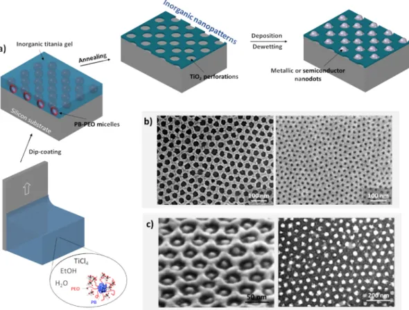
The strategy used to prepare the organized nanodot arrays is illustrated in Figure 1, together with the SEM images of the bare INP surface (b) and thefinal nanodots arrays embedded within the perforations (c). As described in theExperimental Section, a self-assembled network of micelles embedded in a titania sol−gel matrix is deposited by dip-coating on a silicon wafer substrate, forming the intermediate hybrid nanopatterns (Figure 1a). After annealing, a network of circular perforations, in place of the micelles, is obtained through decomposition of the organic copolymers and densification, crystallization, and diffusive sintering of the inorganic TiO2 network.44 The
surface of the substrate is clearly visible through the perforations (see Figure 1b). This dip-coating method is highly scalable as it is possible to deposit on a surface of several cm2in a few seconds. The nanoperforations of the titania layer form a compact hexagonal lattice on a length scale of few micrometers while, at a larger scale, hexagonal domains with different orientations are found. With the copolymer PB12.5 -b-PEO15, perforations have a diameter of 20 ± 3 nm with a
spacing of 40 nm between perforations (center-to-center). The thickness of the INPs was measured to be 7 nm with a refractive index nλ= 1.66 + 0.05/λ2, lower than bulk TiO
2as
expected for a perforated layer. Smaller perforations 12± 2 nm
(spacing ≈ 30) can be obtained with a smaller block
copolymer (i.e., PB5.5-b-PEO30).
Figure 1.(a) Scheme representing the process used to obtain organized metallic or semiconductor nanodots. A monolayer of micelles embedded in a titania gel isfirst deposited on a silicon substrate. After annealing, TiO2inorganic nanopatterns are formed revealing the bare silicon. In the
appropriate conditions (discussed later), a single nanodot per perforation is obtained. (b) SEM images of the TiO2INPs network after annealing
for (left) large perforations of 20 nm (PB12.5-b-PEO15), (right) small perforations of 12 nm (PB5.5-b-PEO30). (c) SEM images of nanodots
The topography and/or the chemical potential affinities between the deposited inorganic layer and the bare surface of the substrate underneath will be used to obtain perfectly organized metallic or semiconductor nanodots (Figure 1c). A careful tuning of the process parameters, from sample preparation to postannealing treatments, is necessary to control the INP structure.
3.1. Removal of the Native Silicon Oxide Layer. The substrate surface, accessible through the perforations, is silicon dioxide (SiO2) originating from the INPs formation process.
To remove the oxide layer, typically of a thickness of about 2 nm, the substrates are immersed into a solution of diluted HF (1.17 mol L−1) for 20 s. The duration is optimized to remove the silicon oxide thickness without damaging the INPs. Indeed, titania is also dissolved by HF but at a lower speed than SiO2.
Besides, the resistance of TiO2to HF is highly dependent on the INP annealing temperature.Figure 2 shows that for a 30 min annealing at 350°C the INPs are totally removed after a HF treatment of 20 s. Only partial damages are visible on the INPs network after a similar treatment at 400°C, whereas no damage can be seen for an annealing at 450°C. Crystallization in anatase of sol−gel based titania is known to start at 300 °C while extended crystal growth occurs at higher temperature through diffusive sintering.38,50 A high degree of crystallinity (larger grains with lower density of grain boundary) is thus necessary to sustain the HF treatment applied to remove the silica native layer. However, even in these conditions, if the etching duration exceeds 40 s, the INPs network is totally removed from the surface, likely due to the attack of the SiO2
layer underneath the INP network, triggering its liftoff. Once the oxide layer is removed from the inside of the perforations, the substrates are immediately placed under vacuum to avoid the oxidation of the bare silicon surface. At this point, the diameter of the perforations is measured to be 28± 4 nm.
3.2. Optimization of Ge Deposition Parameters. To use the titania perforation as a template for Ge nanodots localization, the MBE deposition process consists of three steps (seeFigure 3). First, a predeposition annealing (“flash”: 450 °C for 20 min) is used to promote surface impurities desorption. This stage leads also to the transformation of anatase TiO2 into rutile as deduced from subsequent XRD analysis. Even if the transition from anatase to rutile is generally expected above 600°C for thin films,50we suppose
that ultrahigh-vacuum conditions promote the diffusion
enough to lead to this transition at a temperature as low as
450 °C. Then, 2 nm of Ge is deposited at a substrate
temperature Tev. Finally, the substrate is annealed at a
temperature Tanduring tanto facilitate dots ripening.
The deposition temperature Tev promotes the diffusion of
adatoms. This diffusion can be limited by the surface
roughness and the associated energetic barriers. In this case, nanodot nucleation centers will correspond to local energetic
minima. They can be located on the titania layer. To allow the diffusion of the adatoms to the absolute energetic minima position (bare silicon in titania layer perforation), Tevmust be
high enough.
To assess the state of the surface after germanium deposition, the number of Ge nanodots in the perforations (N1Ge) and on the titania (N2Ge) is evaluated on SEM images.
Figure 4 gives an overview of the pictures used for the statistical count. An entire scan of the surface reveals that
Figure 2.SEM images of INPs surfaces: (a) before HF etching and (b−d) after immersion in HF (1.17 mol L−1) for 20 s. The INPs were calcined at 350 (b), 400 (c), and 450°C (d) for 30 min before HF treatment.
Figure 3.Scheme representing the process parameters of the Ge MBE deposition. Parameters that are varied during the study are written in red. After HF treatment, the substrate is introduced in the chamber. A flash thermal treatment is systematically performed to remove impurities, followed by Ge evaporation at a substrate temperature Tev, followed by an annealing of the deposited layer at a temperature
Tanand a duration tan.
Figure 4.SEM images of the TiO2INPs surface after the deposition
of 2 nm of germanium in various conditions summarized inTable 1: (a) Germanium deposition with a growth temperature Tev= 20°C,
followed by an in situ thermal annealing at Tan= 450°C during tan=
20. (b) Same conditions as in (a) but for an annealing time tan= 2 h.
(c) Same conditions as in (a) but for an annealing temperature Tan=
650°C. (d) Same conditions as in (c) but for a growth temperature Tev = 450 °C. (e) Same conditions as in (c) but for a growth
theses samples are homogeneous. For a given area, covering at least 150 dots for each measurement, the percentage of coverage (%cov= N1Ge/(N2Ge+ N1Ge)) is calculated. If nanodots
are only found in the perforations, %cov = 100%. Different
deposition conditions are investigated (seeTable 1), and the results are summarized inFigure 4.
In all the investigated samples, one dot per perforation is always found while the number of dots found on the titania surface is variable. At room temperature deposition (Tev= 20
°C), almost as many dots are found on the INPs network than in the perforations (sample a). The effect of the postdeposition annealing treatment is weak. For Tan= 450°C, increasing the annealing time from 20 min to 2 h (sample b) only increases the coverage ratio from 55% to 64%. Besides, for tan= 20 min, increasing the annealing temperature Tanto 650°C (sample c)
leads to 58% coverage. These experiments demonstrate that Ge adatoms cannot overcome energetic barriers at room temperature and nucleate on local energetic minima. More-over, once nanodots are formed, they are stable: no ripening is observed during postdeposition annealing.
To promote the placement of the dots solely in the perforations, a higher deposition temperature is required. For Tev = 450 °C (sample d) a coverage of 78% is obtained. A
perfect coverage of 100% is found for Tev = 650°C with Ge dots only in the perforations (see Figures 1c and 4e). This result shows that the mobility of germanium can only be promoted during the nucleation step, before the formation and growth of Ge crystals on TiO2. Above a threshold temperature, germanium can overcome the energetic diffusion barriers of TiO2surface, allowing the diffusion of Ge adatoms toward Si: nanodots nucleation occurs inside the perforations. The process is probably assisted by the morphological evolution of the titania layer. Increasing the temperature, the number of defects on the TiO2INPs decreases: TiO2crystallites grow in size through diffusive sintering which reduce the number of grains boundaries and the overall number of defects. This kind of phenomenon has been studied, regarding the nucleation and growth of germanium nanocrystals on focused ion beam patterned silicon and silica substrates.26,27 However, in the present work, many surface energies are involved and the sample topography is entangled, complicating a possible modelization.
3.3. Advanced Characterization of Ge Dots. The perfect disposition of Ge nanodots is driven by the germanium affinity for the Si substrate. This result suggests that the SiO2
underlayer formed during titania deposition is totally dissolved by the HF acid etching, inside TiO2perforation. Therefore, an
epitaxial relationship is expected between germanium and silicon lattices. It has been investigated by XRD and HRTEM.
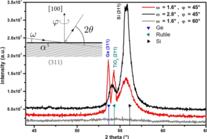
The XRD analysis is shown in Figure 5. As no detectable diffraction peaks were obtained in Bragg−Brentano geometry,
only GIXRD is shown. This indicates either very few crystallized volume or highly texturedfilm (preferred crystallo-graphic orientation along specific directions). GIXRD reveals the presence of diffraction peaks only around 2θ = 55°; the peak intensities depend on both the in-plane (φ) and incident angle (ω). The inset in Figure 5 is a schematic view of the GIXRD geometry. To observe the diffraction peaks of silicon and germanium in GIXRD, several points have to be taken into account: (i) In this configuration, at φ = 0°, the in-plane orientation of the Si (100) substrate is along the [010] direction; in a cubic system, the (311) planes are thus atφ = 45°. (ii) In a cubic system, the angle between the (100) and (311) planes isα = 25.24°. (iii) The theoretical 2θ angle for (311) reflections is 2θ = 53.68° for relaxed Ge and 2θ = 56.12° for relaxed Si. Considering the GIXRD geometry, the corresponding diffraction peaks should appear for incident angles ofω = 1.6° for Ge (311) and ω = 2.8° for Si (311). GIXRD measurements were thus recorded withω around 1.5° andφ = 45° to detect the (311) planes. Experimentally,Figure 5 clearly shows that the diffraction peaks are only visible around 2θ = 55° and that the diffraction peaks disappear when the sample is rotated in plane (φ ≠ 45°) as expected for an heteroepitaxial system. Moreover, Ge (311) peak detection is
optimized at ω = 1.6. Concerning the Si (311) Bragg
reflection, it is also detectable at incident angle of ω = 1.6° due to the X-ray beam average divergence and the huge substrate signal. At ω = 2.8°, the Si (311) reflection is
optimized and the peak at 2θ = 54.1° corresponds to an
average between the Ge (311) and TiO2 (211) reflection, these peaks being clearly dissociated when the incident angle is 1.6°. This analysis thus confirms the unique Ge crystallite orientation, with (100) plane parallel to the Si substrate (100) plane. However, the experimental resolution does not allow determine the possible strain induced by the epitaxial relationship. Depending on the presence of dislocations, the germanium lattice can be either in a tensile strain or relaxed.
HRTEM analyses were performed not only to confirm the
epitaxial relationship between Ge dots and the silicon substrate Table 1. Resulting Placement of the Nanodots for Various
Growth TemperatureTevduring the Deposition of 2 nm of
Germanium, Followed by Different Annealing Conditions
(TemperatureTan, Durationtan)a
a b c d e
Tev(°C) 20 20 20 450 650
Tan(°C) 450 450 650 650 650
tan 20 min 2 h 20 min 20 min 20 min
%cov(%) 55 64 58 78 100
aLetters in thefirst row corresponds to the SEM images inFigure 4.
Figure 5. XRD analysis of TiO2 INPs bearing Ge nanocrystals:
patterns recorded in GIXRD geometry with two different incident (ω) and in plane (φ) angles (in plane angle is measured from the Si substrate [010] direction). The triangle markers indicate the theoretical positions of Bragg reflections related to Ge, rutile TiO2,
but also to research the presence of structural defects at the Si−Ge interface (seeFigure 6). Ge dots are in epitaxy on the
silicon wafer, inside the perforations, in agreement with XRD analysis. On either side, the rutile TiO2crystallites of the INPs
are present, with the underlying thin SiO2layer. At the location of the Ge dot, in the perforation, the atomic lattice of Ge is seen to extend up to the crystalline surface of silicon. The monocrystalline nature of germanium is clearly visible and confirmed by Fourier transformation. Moreover, facets are
visible with no apparent defects confirming the perfect
heteroepitaxy of the Ge nanocrystals on silicon and the tensile strain induced by the silicon substrate. Considering the growth and annealing conditions of the germanium dots on the silicon wafer, a limited interdiffusion of Ge and Si at interface is likely to occur.
3.4. Variation in the INPs Network Parameters: Smaller Perforations. Finally, to prove theflexibility of the proposed inorganic nanoperforations, deposition of
germa-nium was performed on TiO2 INPs bearing smaller
perforations. To obtain such prepatterned surfaces, the same protocol was followed with a smaller block copolymer: PB5.5 -b-PEO30. The well-ordered perforated network is visible as seen
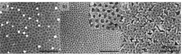
for the larger perforations (seeFigure 1b). The mean diameter, deduced from SEM, is 12± 2 nm. Deposition was performed following the procedure optimized for larger perforations (HF treatment 20 s, 2 nm of Ge deposited at 650°C then annealing at 650 °C for 20 min). SEM imaging after deposition shows that one Ge crystal is found in each perforation with a few large Ge dots visible on the TiO2network (Figure 7a). This corresponds to a %cov= 92%. Thus, it seems that in the case of
smaller perforations a deposition at a temperature of 650 °C does not give enough mobility to Ge to diffuse entirely toward
the perforations even if the interdistance between perforations is smaller. The temperature was then gradually increased until no dots were found on the INPs surface. At a temperature of 800 °C, the INPs network starts to lose organization with a collapse of the INPs structure due to extensive diffusive sintering (Figure 7c). Ge dots, originally located in the
perforations, merge to form larger dots as the TiO2
topographical barrier is breaking apart. We note that in this case no Ge dots are found on the INPs.
A narrow window thus seems to exist with full organization
of germanium in the perforations before the TiO2 INPs
become unstable. Results of deposition at 775 °C show
organized Ge dots with full diffusion in the perforations (Figure 7b). The TiO2 network begins to collapse, but the extent is not large enough to allow the Ge dots to merge. In this case, a percentage of coverage of 98% is found with very few dots on the INPs. The average diameter of the dots on the INPs is about the same than the ones in the perforations in contrast with the previous case (Ge deposition at 650°C). The very small size of the Ge dots embedded in the perforations did not allow to obtain SEM images with sufficient resolution to extract a size distribution. Nevertheless, as Ge crystals are located within the INPs perforations, their size diameter is bound to be smaller than the one of the perforation (12± 2 nm) and can be roughly estimated to 9± 3 nm. Note that in the case of smaller perforations the annealing step after evaporation (seeFigure 3) was suppressed from the process as similar results were obtained with or without postannealing. Because the temperature is maintained for a shorter time, this allows to work at higher temperature without damaging too much the INPs.
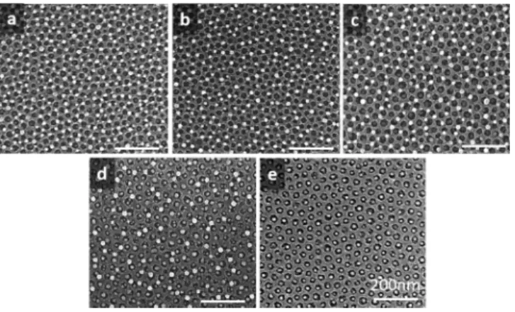
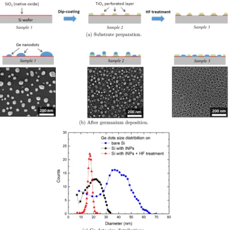
3.5. Comparison Spontaneous/Directed Deposition. If deposition takes place on a nonpatterned surface, randomly dispersed islands with a large size distribution are expected (Figure 8a). For instance, the deposition of a 2 nm thick layer
of germanium (at 650 °C under ultrahigh vacuum and
annealed at 650°C for 20 min) on bare silica gives Ge dots of an average diameter of 40 nm with a very large diameter distribution ranging from 10 to 65 nm (Figure 8d).
To direct the Ge atoms diffusion and reduce size
distribution, prepatterning of the surface is thus necessary. In our case, deposition and annealing are performed on inorganic nanopatterns. Without any additional treatment, Ge nanodots feature a narrower size distribution than for spontaneous deposition (Figure 8b). An average diameter of 23± 10 nm is reported in accordance with previous studies.19 Indeed, with this additional surface texturing, the presence of energetically favorable points leads to a more homogeneous size distribution with respect to the spontaneous deposition case. However, even if the size distribution is drastically reduced compared to a flat surface, no precise spatial organization is found. To
Figure 6. TEM analysis of Ge dots in TiO2 perforations with
corresponding Fourier transform. Facets are easily visible on the Ge crystals.
Figure 7.SEM images of the TiO2INPs after the deposition of 2 nm
of germanium at different temperatures: (a) deposition at 650 °C, (b) deposition at 775°C, and (c) deposition at 800 °C. No annealing is performed after deposition. The scale bar is 200 nm.
obtain a precise organization of the dots, the position of defects must be controlled, which could be the case with the INPs network as it bears organized perforations. Nevertheless, without any additional treatment, the bottom of the
perforations still consist of silicon oxide, which displays a
low affinity with germanium. In fine, Ge nanodots will
preferably nucleate on the TiO2INPs network where defects,
such as grain boundaries between rutile crystals, will locally
Figure 8.Deposition and dewetting of 2 nm of Ge at 650°C followed by annealing at 650 °C for 20 min: (a) substrate preparation; (b) SEM image after germanium deposition on a bare silicon surface (sample 1), TiO2 INPs without chemical etching (sample 2), TiO2 INPs after
appropriate etching (sample 3); (c) corresponding germanium dots diameter distribution.
Figure 9.SEM images of (a) TiO2INPs after the deposition of a thin Au layer, (b) TiO2INPs with Au droplets after annealing at 450°C for 30
min in ultrahigh vacuum, and (c) TiO2INPs with Au droplets after annealing and mechanical etching. Insets display the corresponding Fourier
increase the surface energy, providing narrow size distribution but no organization.
In contrast, with the appropriate HF chemical etching, the silicon oxide can be eliminated from the bottom of the perforations revealing the silicon surface while keeping the TiO2 structure intact (Figure 2). Silicon is a convenient nucleation point for Ge growth since Ge is highly miscible in Si. Taking advantage of the chemical heterogeneity brought by
the TiO2 INPs and in optimized deposition conditions
discussed above, nucleation and growth of Ge nanodots can be controlled leading to one dot per perforation (Figure 8c). A sharp size distribution of 17± 2 nm is found without any dot on the INPs network. Ge nanocrystals, in epitaxy with the silicon substrate, are well organized in a hexagonal lattice with
their diameter and spacing defined by the INPs network
parameters.
3.6. Organization of Au Nanoparticles. TiO2INPs are
now used as a prepattern surface for the organization of metallic nanoparticles. For this purpose, a thin gold layer of 3.5 nm is deposited by sputtering on the TiO2 nanoperforated layer. Even before annealing, the gold layer broke down into islands of various size and shape that cover the entire substrate (Figure 9a). This is expected as the mobility of metals is higher than the one of semiconductors.51−56 The presence of the TiO2 network can be guessed with smaller islands inside the
perforations and large elongated islands on the network. To obtain more homogeneous Au domains, an annealing step is performed in an epitaxy chamber under ultrahigh
vacuum (P = 10−10 Pa) at 450 °C for 30 min. In those
conditions, Au thin layers are known to dewet and form isolated islands.10The film after annealing shows round gold
droplets confirming the high mobility of gold at this
temperature (Figure 9b). A large size distribution of the Au dots is found with size ranging from 10 to 45 nm (Figure 9d). Moreover, dots are randomly arranged without any specific interaction with the bottom of the perforations (silicon) or with the INPs network (TiO2). This is due to the fact that Au
does not have a specific affinity for silicon compared to TiO2. In this case, only topographical defects are directing the atomic diffusion, which is not sufficient to directly obtain organized arrays of dots in contrast with germanium deposition process. As ordering of Au dots could not be obtained solely via deposition and annealing, abrasion of the surface by gently polishing with a fabric revealed to be efficient to remove the dots on the TiO2without impacting those formed within the perforations. Indeed, as gold has a poor affinity for the surface, it can be easily removed mechanically. By polishing the surface, only the raised areas will be impacted: the Au dots on top of the INPs. In this case, the INPs network behave as a topographical mask that selectively protect the Au dots in the perforations.Figure 9c presents the image of the surface where only Au dots in the perforations are left after polishing with clean room paper. The repeatability of this polishing step was assessed on several 2 in. wafers and controlled by SEM on the whole surface. In addition, the influence of the force used for polishing was optimized to 0.75 N cm−2 to remove only the dots sitting on the perforations. Nice organization with hexagonal arrangement is found corresponding to the INPs network parameter as confirmed by Fourier transformation (FT). The size distribution of the Au dots after such mechanical treatment is 28± 5 nm in diameter, which is in good agreement with the size of the perforations (Figure 9d). The slight broadening toward smaller dots can be explained by
the fact that not all the perforations are fullyfilled by gold. For comparison, if deposition of a thin Au layer is performed on bare silicon, a very large size distribution with dots of diameter about roughly 30 times the Au deposited thickness is found.10 In the present case of a 3.5 nm Au layer, this translates into droplets of about 100± 50 nm in diameter.
Furthermore, in the case of metals, as only a topographical control is used, HF chemical treatment is not compulsory to organize the Au dots. However, revealing the silicon surface at the bottom of the perforations is important to have an interface between gold and silicon for instance in the case Au dots are further used as VLS catalysts to obtain out-of-plane nanowires. In addition, such surfaces are expected to be interesting for surface-enhanced Raman scattering (SERS) due to their unique organization.
4. CONCLUSION
TiO2 inorganic nanopatterns proved to be an exceptional pretemplated surface for the directed ordering of both semiconductor and metallic nanodots. In the case of germanium thin layers, selective epitaxy of Ge on the bare silicon within the perforations allowed to organize the Ge nanodots after HF chemical treatment and in optimized deposition conditions. The concentration of the HF bath has been optimized to remove the silicon oxide in a manageable delay, with a sufficient time window before damaging the TiO2 network. This technique, performed routinely in the micro-electronic industry, turned out efficient in terms of selectivity and uniformity.
Highly organized sub-100 nm germanium nanocrystals were obtained in epitaxy, with a sharp size distribution, proving that the Ge nanodots network obtained can be dedicated to optoelectronic applications. This is a huge improvement compared to stochastic nucleation of Ge on Si. Moreover, we proved that the density and organization of the nanodots can be easily tailored by changing the INPs network parameters.
Next, TiO2 INPs were also exploited to control gold
deposition. The organization was no more brought by the affinity between Au and Si, but with an appropriate polishing of the surface. The resulting nanodots were organized with again a tunable narrow size distribution. Nevertheless, the HF treatment was maintained to ensure a clean silicon−gold interface which is critical for vapor−liquid−solid growth process. This open the way for a better control of nanowires size distribution and organization. But it is also an advance for plasmonic or charge transfer for photoinduced electrochemical processes.
The INPs template fabrication is flexible. Copolymer self-assembly can yield triangular or square domains and can be easily extended to other inorganic materials like SiO2, ZnO, or
CaTiO3. This technique prove to be a promising way for innovative applications.
■
AUTHOR INFORMATIONCorresponding Author
*E-mail [email protected]; Ph +33 (0)4 91 28 91 59; Fax +33 (0)4 91 28 91 61.
ORCID
Thomas Bottein:0000-0003-0312-2057
Mohammed Bouabdellaoui:0000-0003-0980-4104 Jean-Benoît Claude:0000-0001-9618-0576
Luc Favre:0000-0002-9010-0085 Thomas David: 0000-0002-6796-220X Magali Putero:0000-0001-6527-4334 Marco Abbarchi:0000-0002-2760-4766 David Grosso: 0000-0002-9156-6848 Notes
The authors declare no competingfinancial interest.
■
ACKNOWLEDGMENTSThe authors acknowledge the funding by A*MIDEX
(reference ANR- 11-IDEX-0001-02) and MATISSE and the facilities of the NANOTECMAT platform at the IM2NP and of the CP2M of Aix-Marseille University.
■
REFERENCES(1) O’Regan, B.; Grätzel, M. A Low-Cost, High-Efficiency Solar Cell Based on Dye-Sensitized Colloidal TiO2 Films. Nature 1991, 353,
737−740.
(2) Aberg, I.; Vescovi, G.; Asoli, D.; Naseem, U.; Gilboy, J. P.; Sundvall, C.; Dahlgren, A.; Svensson, K. E.; Anttu, N.; Bjork, M. T.; Samuelson, L. A GaAs Nanowire Array Solar Cell with 15.3% Efficiency at 1 Sun. IEEE Journal of Photovoltaics 2016, 6, 185−190. (3) Tian, B.; Zheng, X.; Kempa, T. J.; Fang, Y.; Yu, N.; Yu, G.; Huang, J.; Lieber, C. M. Coaxial Silicon Nanowires as Solar Cells and Nanoelectronic Power Sources. Nature 2007, 449, 885−889.
(4) Dasary, S. S.; Singh, A. K.; Senapati, D.; Yu, H.; Ray, P. C. Gold Nanoparticle Based Label-Free SERS Probe for Ultrasensitive and Selective Detection of Trinitrotoluene. J. Am. Chem. Soc. 2009, 131, 13806−13812.
(5) Shiraki, Y.; Sunamura, H.; Usami, N.; Fukatsu, S. Formation and Optical Properties of SiGe/Si Quantum Structures. Appl. Surf. Sci. 1996, 102, 263−271.
(6) Yakimov, A. I.; Dvurechenskii, V. A.; Kirienko, V. V.; Yakovlev, Y. I.; Nikiforov, A. I.; Adkins, C. J. Long-Range Coulomb Interaction in Arrays of Self-Assembled Quantum Dots. Phys. Rev. B: Condens. Matter Mater. Phys. 2000, 61, 10868−10876.
(7) Choi, W. K.; Liew, T. H.; Chew, H. G.; Zheng, F.; Thompson, V. C.; Wang, Y.; Hong, M. H.; Wang, X. D.; Li, L.; Yun, J. A Combined Top-Down and Bottom-Up Approach for Precise Placement of Metal Nanoparticles on Silicon. Small 2008, 4, 330−333.
(8) Zhang, X.; Qiao, Y.; Xu, L.; Buriak, J. M. Constructing Metal-Based Structures on Nanopatterned Etched Silicon. ACS Nano 2011, 5, 5015−5024.
(9) Altomare, M.; Nguyen, N. T.; Schmuki, P. Templated Dewetting: Designing Entirely Self-Organized Platforms for Photo-catalysis. Chemical Science 2016, 7, 6865−6886.
(10) Benkouider, A.; Ronda, A.; David, T.; Favre, L.; Abbarchi, M.; Naffouti, M.; Osmond, J.; Delobbe, A.; Sudraud, P.; Berbezier, I. Ordered Arrays of Au Catalysts by FIB Assisted Heterogeneous Dewetting. Nanotechnology 2015, 26, 505602.
(11) Nitta, Y.; Shibata, M.; Fujita, K.; Ichikawa, M. Nanometer-Scale Ge Selective Growth on Si (001) Using Ultrathin SiO Film. Surf. Sci. 2000, 462, L587.
(12) Leroy, F.; Eymery, J.; Gentile, P.; Fournel, F. Surf. Sci. 2003, 545, 211−219.
(13) Berbezier, I.; Ronda, A.; Portavoce, A.; Motta, N. Ge Dots Self-Assembling: Surfactant Mediated Growth of Ge on SiGe (118) Stress-Induced Kinetic Instabilities. Appl. Phys. Lett. 2003, 83, 4833−4835. (14) Essolaani, W.; Picaud, F.; Ramseyer, C.; Gambardella, P.; Saïd, M.; Spanjaard, D.; Desjonquères, M. C. Formation of One-Dimensional Ordered Alloy at Step Edges: an Atomistic Study of the (2× 1) Ni/Pt Alloy on he Pt(997) Surface. Surf. Sci. 2011, 605, 917−922.
(15) Pascale, A.; Berbezier, I.; Ronda, A.; Videcoq, A.; Pimpinelli, A. Self-Organization of Step Bunching Instability on Vicinal Substrate. Appl. Phys. Lett. 2006, 89, 104108.
(16) Berbezier, I.; Ronda, A. Self-Assembling of Ge Dots on Nanopatterns: Experimental Investigation of Their Formation, Evolution and Control. Phys. Rev. B: Condens. Matter Mater. Phys. 2007, 75, 1−10.
(17) Spinelli, P.; Verschuuren, M. A.; Polman, A. Broadband Omnidirectional Antireflection Coating Based on Subwavelength Surface Mie Resonators. Nat. Commun. 2012, 3, 692.
(18) Masuda, H.; Fukuda, K. Ordered Metal Nanohole Arrays Made by a Two-Step Replication of Honeycomb Structures of Anodic Alumina. Science 1995, 268, 1466−1468.
(19) Rowell, N. L.; Lockwood, D. J.; Amiard, G.; Favre, L.; Ronda, A.; Berbezier, I.; Faustini, M.; Grosso, D. Photoluminescence Efficiency and Size Distribution of Self Assembled Ge Dots on Porous TiO2. J. Nanosci. Nanotechnol. 2011, 11, 9190−9195.
(20) Lockwood, D.; Rowell, N.; Barbagiovanni, E.; Goncharova, L.; Simpson, P.; Berbezier, I.; Favre, L.; Amiard, G.; Ronda, A.; Faustini, M.; Grosso, D. Photoluminescence Efficiency of Germanium Dots Self-Assembled on Oxides. ECS Trans. 2013, 53, 185−206.
(21) Bublat, T.; Goll, D. Large-Area Hard Magnetic L10-FePt Nanopatterns by Nanoimprint Lithography. Nanotechnology 2011, 22, 315301.
(22) Wang, D.; Ji, R.; Schaaf, P. Formation of Precise 2D Au Particle Arrays via Thermally Induced Dewetting on Pre-Patterned Substrates. Beilstein J. Nanotechnol. 2011, 2, 318−326.
(23) Giermann, A. L.; Thompson, V. C. Solid-State Dewetting for Ordered Arrays of Crystallographically Oriented Metal Particles. Appl. Phys. Lett. 2005, 86, 121903.
(24) Abbarchi, M.; Naffouti, M.; Vial, B.; Benkouider, A.; Lermusiaux, L.; Favre, L.; Ronda, A.; Bidault, S. S.; Berbezier, I.; Bonod, N. Wafer Scale Formation of Monocrystalline Silicon-Based Mie Resonators via Silicon-On-Insulator Dewetting. ACS Nano 2014, 8, 11181−11190.
(25) Aouassa, M.; Berbezier, I.; Favre, L.; Ronda, A.; Bollani, M.; Sordan, R.; Delobbe, A.; Sudraud, P. Design of Free Patterns of Nanocrystals with Ad Hoc Features via Templated Dewetting. Appl. Phys. Lett. 2012, 101, 013117.
(26) Karmous, A.; Cuenat, A.; Ronda, A.; Berbezier, I.; Atha, S.; Hull, R. Ge Dot Organization on Si Substrates Patterned by Focused Ion Beam. Appl. Phys. Lett. 2004, 85, 6401−6403.
(27) Karmous, A.; Berbezier, I.; Ronda, A. Formation and Ordering of Ge Nanocrystals on SiO_{2}. Phys. Rev. B: Condens. Matter Mater. Phys. 2006, 73, No. 075323.
(28) Naffouti, M.; Backofen, R.; Salvalaglio, M.; Bottein, T.; Lodari, M.; Voigt, A.; David, T.; Benkouider, A.; Fraj, I.; Favre, L.; Ronda, A.; Berbezier, I.; Grosso, D.; Abbarchi, M.; Bollani, M. Complex Dewetting Scenarios of Ultrathin Silicon Films for Large-Scale Nanoarchitectures. Sci. Adv. 2017, 3, 1472−1482.
(29) Abbarchi, M.; Naffouti, M.; Lodari, M.; Salvalaglio, M.; Backofen, R.; Bottein, T.; Voigt, A.; David, T.; Claude, J.-B.; Bouabdellaoui, M.; Benkouider, A.; Fraj, I.; Favre, L.; Ronda, A.; Berbezier, I.; Grosso, D.; Bollani, M. Solid-State Dewetting of Single-Crystal Silicon on Insulator: Effect of Annealing Temperature and Patch Size. Microelectron. Eng. 2018, 190, 1−6.
(30) Kim, H. C.; Park, S. M.; Hinsberg, W. D. Block Copolymer Based Nanostructures: Materials, Processes, and Applications to Electronics. Chem. Rev. 2010, 110, 146−177.
(31) Grosso, D.; Ribot, F.; Boissiere, C.; Sanchez, C. Molecular and Supramolecular Dynamics of Hybrid Organic-Inorganic Interfaces for the Rational Construction of Advanced Hybrid Nanomaterials. Chem. Soc. Rev. 2011, 40, 829−848.
(32) Dimitrov, A. S.; Nagayama, K. Continuous Convective Assembling of Fine Particles into Two-Dimensional Arrays on Solid Surfaces. Langmuir 1996, 12, 1303−1311.
(33) Kadiri, H. Auto-Organisation Assistée pour la Nano-Impression à Grande Échelle et Surfaces Optiques Multifonctionnelles. Ph.D. Thesis, 2017.
(34) Ghicov, A.; Schmuki, P. Self-Ordering Electrochemistry: a Review on Growth and Functionality of TiO2Nanotubes and Other
(35) Faustini, M.; Marmiroli, B.; Malfatti, L.; Louis, B.; Krins, N.; Falcaro, P.; Grenci, G.; Laberty-Robert, C.; Amenitsch, H.; Innocenzi, P.; Grosso, D. Direct Nano-In-Micropatterning of TiO2Thin Layers
and TiO2/Pt Nanoelectrode Arrays by Deep X-Ray Lithography. J.
Mater. Chem. 2011, 21, 3597−3603.
(36) Faustini, M.; Drisko, G. L.; Letailleur, A. A.; Montiel, R. S.; Boissière, C.; Cattoni, A.; Haghiri-Gosnet, A. M.; Lerondel, G.; Grosso, D. Self-Assembled Titanium Calcium Oxide Nanopatterns as Versatile Reactive Nanomasks for Dry Etching Lithographic Transfer with High Selectivity. Nanoscale 2013, 5, 984−990.
(37) Kuemmel, M.; Allouche, J.; Nicole, L.; Boissière, C.; Laberty, C.; Amenitsch, H.; Sanchez, C.; Grosso, D. A Chemical Solution Deposition Route to Nanopatterned Inorganic Material Surfaces. Chem. Mater. 2007, 19, 3717−3725.
(38) Faustini, M.; Nicole, L.; Boissière, C.; Innocenzi, P.; Sanchez, C.; Grosso, D. Hydrophobic, Antireflective, Self-Cleaning, and Antifogging Sol-Gel Coatings: an Example of Multifunctional Nanostructured Materials for Photovoltaic Cells. Chem. Mater. 2010, 22, 4406−4413.
(39) Laberty-Robert, C.; Kuemmel, M.; Allouche, J.; Boissière, C.; Nicole, L.; Grosso, D.; Sanchez, C. Sol-Gel Route to Advanced Nanoelectrode Arrays (NEA) Based on Titania Gold Nano-composites. J. Mater. Chem. 2008, 18, 1216.
(40) Martínez-Ferrero, E.; Forneli, A.; Boissière, C.; Grosso, D.; Sanchez, C.; Palomares, E. Tailored 3D Interface for Efficiency Improvement in Encapsulation-Free Hybrid Light-Emitting Diodes. ACS Appl. Mater. Interfaces 2011, 3, 3248−3251.
(41) Lepoutre, S.; Grosso, D.; Sanchez, C.; Fornasieri, G.; Rivière, E.; Bleuzen, A. Tailor-Made Nanometer-Scale Patterns of Photo-Switchable Prussian Blue Analogues. Adv. Mater. 2010, 22, 3992− 3996.
(42) Neu, V.; Schulze, C.; Faustini, M.; Lee, J.; Makarov, D.; Suess, D.; Kim, S.-K.; Grosso, D.; Schultz, L.; Albrecht, M. Probing the Energy Barriers and Magnetization Reversal Processes of Nano-perforated Membrane Based Percolated Media. Nanotechnology 2013, 24, 145702.
(43) Schulze, C.; Faustini, M.; Lee, J.; Schletter, H.; Lutz, M. U.; Krone, P.; Gass, M.; Sader, K.; Bleloch, a. L.; Hietschold, M.; Fuger, M.; Suess, D.; Fidler, J.; Wolff, U.; Neu, V.; Grosso, D.; Makarov, D.; Albrecht, M. Magnetic Films on Nanoperforated Templates: a Route Towards Percolated Perpendicular Media. Nanotechnology 2010, 21, 5701−5710.
(44) Faustini, M.; Grosso, D. Self-Assembled Inorganic Nano-patterns (INPs) Made by So-Gel Dip-Coating: Applications in Nanotechnology and Nanofabrication. C. R. Chim. 2016, 19, 248− 265.
(45) Kuemmel, M.; Smått, J.-H.; Boissière, C.; Nicole, L.; Sanchez, C.; Lindén, M.; Grosso, D. Hierarchical Inorganic Nanopatterning (INP) through Direct Easy Block-Copolymer Templating. J. Mater. Chem. 2009, 19, 3638.
(46) Hughes, R. A.; Menumerov, E.; Neretina, S. When Lithography Meets Self-Assembly: a Review of Recent Advances in the Directed Assembly of Complex Metal Nanostructures on Planar and Textured Surfaces. Nanotechnology 2017, 28, 282002.
(47) Thompson, C. V. Solid-State Dewetting of Thin Films. Annu. Rev. Mater. Res. 2012, 42, 399−434.
(48) Kim, H. J.; Lee, S. H.; Upadhye, A. A.; Ro, I.; Tejedor-Tejedor, M. I.; Anderson, M. A.; Kim, W. B.; Huber, G. W. Plasmon-Enhanced Photoelectrochemical Water Splitting with Size-Controllable Gold Nanodot Arrays. ACS Nano 2014, 8, 10756−10765.
(49) Wu, B.; Liu, D.; Mubeen, S.; Chuong, T. T.; Moskovits, M.; Stucky, G. D. Anisotropic Growth of TiO2onto Gold Nanorods for
Plasmon-Enhanced Hydrogen Production from Water Reduction. J. Am. Chem. Soc. 2016, 138, 1114−1117.
(50) Louis, B.; Krins, N.; Faustini, M.; Grosso, D. Understanding Crystallization of Anatase into Binary SiO2/TiO2 Sol-Gel Optical
Thin Films: an in situ Thermal Ellipsometry Analysis. J. Phys. Chem. C 2011, 115, 3115−3122.
(51) Slezák, J.; Ondřejček, M.; Chvoj, Z.; Cháb, V.; Conrad, H.; Heun, S.; Schmidt, T.; Ressel, B.; Prince, K. C. Surface diffusion of Au on Si(111): A microscopic study. Phys. Rev. B: Condens. Matter Mater. Phys. 2000, 61, 16121−16128.
(52) Gavrilyuk, Y.; Lifshits, V. Effect of surface phases on the diffusion of gold on silicon. Poverhnost 1983, 4, 82−89.
(53) Dolbak, A. E.; Zhachuk, R. A.; Olshanetsky, B. Z. Surface diffusion of Pb on clean Si surfaces. Cent. Eur. J. Phys. 2004, 2, 254− 265.
(54) Dolbak, A.; Zhachuk, R.; Olshanetsky, B. Mechanism of Cu transport along clean Si surfaces. Open Phys.s 2003, 1, 463−473.
(55) Dolbak, A.; Olshanetsky, B.; Stenin, S.; Teys, S.; Gavrilova, T. Effect of nickel on clean silicon surfaces: Transport and structure. Surf. Sci. 1989, 218, 37−54.
(56) Dolbak, A. E.; Olshanetsky, B. Z. Ge diffusion on Si surfaces. Cent. Eur. J. Phys. 2006, 4, 310−317.
![Risiko- & [und] Schutzfaktoren der psychischen Gesundheit humanitärer Einsatzhelfer : eine systematische Literaturübersicht](data:image/gif;base64,R0lGODlhAQABAIAAAP///wAAACH5BAEAAAAALAAAAAABAAEAAAICRAEAOw==)