HAL Id: tel-00949044
https://tel.archives-ouvertes.fr/tel-00949044
Submitted on 19 Feb 2014
HAL is a multi-disciplinary open access
archive for the deposit and dissemination of sci-entific research documents, whether they are pub-lished or not. The documents may come from teaching and research institutions in France or abroad, or from public or private research centers.
L’archive ouverte pluridisciplinaire HAL, est destinée au dépôt et à la diffusion de documents scientifiques de niveau recherche, publiés ou non, émanant des établissements d’enseignement et de recherche français ou étrangers, des laboratoires publics ou privés.
Study and applications of hybrid organic/ inorganic
semiconductor quantum dots in thin films
Hung-Ju Lin
To cite this version:
Hung-Ju Lin. Study and applications of hybrid organic/ inorganic semiconductor quantum dots in thin films. Optics / Photonic. Aix-Marseille Université, 2013. English. �tel-00949044�
National Central University, Taiwan
Department of Optics and Photonics College of Science
Study and applications of hybrid organic/
inorganic semiconductor quantum
dots in thin films
Hung-Ju LIN
Dissertation submitted for the Doctor of Philosophy degrees
at the National Central University, Taiwan in Science
and
at the Aix-Marseille University, France in Physics and Materials Science
Defended on: December the 12th, 2013
Dissertation committee:
M. Cheng- Chung Lee Professor, National Central University Advisor M. François Flory Professor, Aix-Marseille University Advisor M. Sheng- Hui Chen Professor, National Central University Co-advisor M. Judikaël Le Rouzo Assistant Professor, Aix-Marseille University Co-advisor M. Shiuh Chao Professor, National Tsing Hua University Reviewer M. Yi-Jun Jen Professor, National Taipei University of Technology Reviewer
Aix-Marseille University, France
Equipe Optoélectronique et Photovoltaïque, Institut Matériaux Microélectronique Nanosciences de Provence
i
Abstract
Semiconductor quantum dots have attracted a lot of attention for their potential
application in many fields such as optoelectronics and biology.
In this study, we investigated the optical properties of hybrid nanocomposited
thin films made of PMMA polymer containing different concentrations of
core-shell CdSe/ZnS quantum dots. Both the absorption and luminescence spectra
can be well explained by taking into account quantum mechanisms. From the
luminescence spectral evidence of the coupling effect between quantum dots has
been observed. With a pump laser emitting at 514 nm the luminescence spectrum
centered at 560 nm strongly changes with time.
In addition, it is necessary to control the luminescent light spatial distribution
where the application is concerned. Therefore we proposed structural films with a
bi-periodic grating by nanoimprint technique using an engraved silicon mold. The
characterizations of the imprinted structure show good quality. We also showed,
by a numerical calculation, that the local field is resonant in the periodic structure
ii
Résumé
Semiconductor nanocrystals or quantum dots Les nanocristaux de
semi-conducteurs, ou boites quantiques, trouvent leur application dans de
nombreux domaines. Pendant cette thèse nous avons étudié les propriétés
optiques de couches minces nanocomposites de polymère PMMA contenant
différentes concentrations de boites quantiques CdSe/ZnS. Les spectres
d'absorption et de luminescence peuvent être expliqués par la mécanique
quantique. A partir des spectres de luminescence mesurés nous montrons
clairement l’effet du couplage entre les boites quantiques. Sous l’effet d’un
faisceau pompe à 514nm le spectre de luminescence centré à 560nm évolue
fortement au cours du temps. Nous montrons que ces couches luminescentes qui
convertissent ainsi les fréquences optiques peuvent permettre d’augmenter l’efficacité de cellules solaires. Par ailleurs, pour bénéficier au mieux du fort
rendement de photoluminescence, il est nécessaire de contrôler la répartition
spatiale de la lumière émise. Pour contrôler cette répartition une nanostructure bi
périodique a été réalisée dans des couches de PMMA contenant les boites
quantiques par nano-impression, en utilisant un moule en silicium gravé. La
caractérisation de la structure réalisée met en évidence la qualité de la méthode
utilisée. On montre également, par la théorie, à la fois que le champ local est
résonant dans la structure et que la lumière se répartie en champ lointain dans les
iii
Acknowledgement
Foremost, I would like to express my sincere appreciation to my advisor Prof.
Cheng-Chung Lee and Prof. François Flory, for their patience, enthusiasm, vast
knowledge and their great support throughout my PhD study. I also thank my
co-advisor Prof. Sheng-Hui Chen and Assistant Prof. Judikaël Le Rouzo for
their valuable advices and kind assistances during the research.
Concerning the dissertation committee, I wish to specially thank the reviewers,
Prof. Shiuh Chao and Prof. Yi-Jun Jen, for their detailed review and constructive
comments on this work.
Besides, I would like to thank the French Institute in Taipei and the Office of
International Affairs in National Central University for offering the financial
support in the period of doing research in France.
During this period of two years in France, I wish to thank again to the Prof.
François Flory and Assistant Prof. Judikaël Le Rouzo very much. They always
guided me to deal with some complex works and gave warm consideration for
me. Also I wish to thank all my lab colleagues, for accompanying with me to
create lots of our own impressive and precious memories.
On the other hand, I thank all of my friends for making my life so colorful. In
addition, I sincerely thank everyone who ever gave me a favor during my study.
Finally and most importantly, I am truly grateful to my family for supporting
me to the France and giving me the unstinting source of love. Their love and
iv
Contents
Abstract
…..………iRésumé
…..……….iiAcknowledgement
……….iiiContents
…..………..ivList of figures
…..……….viList of tables
…..………..xv1. Introduction
…..………12. Nanomaterial evolution and nanoimprint technique
…..………....42.1 Development of nanostructured materials…..……….4
2.1.1 Nanostructures in nature……….…....5
2.1.2 Artificially nanostructured materials: semiconductor quantum dots..7
2.1.3 New generation of semiconductor quantum dots...…...11
2.2 Development of nanocomposite thin films………15
2.2.1 Dielectric material contains nanocrystals……….16
2.2.2 Organic polymer containing inorganic nanocrystals………17
2.3 Historic development of nanoimprint lithography………....21
2.3.1 Thermal nanoimprint lithography……….22
2.3.2 UV-curable nanoimprint lithography………24
2.3.3 New material developments……….26
3. Experimental framework and principles
………...283.1 Experimental framework………...28
3.2 Spin coating method – Hybrid thin films/ QDs……….31
3.2.1 Rotational speed and time………....32
3.2.2 Viscosity and concentration of the solution………..33
3.3 Measurement methods………...34
3.3.1 Spectrophotometer- transmission and reflection measurement……34
3.3.2 Photoluminescence measurement……….34
3.3.3 Spectroscopic ellipsometry………...37
v
3.3.4 (a)Transmission electron microscopy………..38
3.3.4 (b)Scanning electron microscopy………40
3.3.5 Atomic force microscopy ………42
4. Hybrid organic thin films/ QDs
………....444.1 PMMA thin film with CdSe/ZnS QDs………..44
4.1.1 Introduction of experimental preparation and processes…………..47
4.1.2 Electron microscopy measurement………...49
4.2 Optical properties of PMMA thin film layers with CdSe/ZnS QDs……..50
4.2.1 Transmission/ reflection and absorption spectrum………...50
4.2.2 Photoluminescence versus wavelengths measurement………56
4.2.3 Photoluminescence intensity versus time measurement…………...61
4.3 Frequency conversion of CdSe/ZnS QDs: Its application to solar cells...72
4.3.1 Using PMMA /QDs films as down-conversion frequency layer….72 4.3.2 QDs embedded in the active layer of organic solar cells………….77
5. Nanostructure d hybrid organic thin films/ QDs
……….815.1 Introduction of thermal nanoimprint organic layers………..81
5.1.1 Heating experiment for transition temperature of organic layers….82 5.1.2 Periodic structure of imprinted pure organic layers……….85
5.2 Imprinted nanostructure in hybrid organic layer with quantum dots……89
5.2.1 Fabrication process of imprinted hybrid layers via optimized heating………89
5.2.2 Periodic structure of imprinted hybrid layers ………..90
5.3 Optical field emission simulation for the periodic nanostructure……….93
5.3.1 Plane wave light emission in the nanostructure………...94
5.3.1(a) Emission light simulation in near field………..94
5.3.1(b) Emission light simulation in far field ………...96
5.3.2 Dipole source emission light in the nanostructure………...98
5.3.2(a) Emission light simulation in near field………..98
5.3.2(b) Emission light simulation in far field………..101
6. Conclusions et perspectives
……….103vi
List of figures
2.1.1: The “Density of States” (DOS) function evolves from a bulk (3D solid)
to a 2D, 1D and 0D system with varying degrees of confinement……..4
2.1.2: (a) SEM image of the surface of a lotus leaf and (b) a higher magnification with hierarchical structures clearly resolved. (c) A water drop on the surface of the lotus leaf attains a nearly spherical shape. (d) SEM image of the artificial laser- structured silanized silicon surface and (e) a higher magnification showing the dual length-scale roughness.
(f) A water drop on the structured surface………...5
2.1.3: SEM images of the butterfly wing (a) and (b), the replicated surface (c)
and (d). Angle of view: 45. The scale bar corresponds to 50 µm on
(a),(c) and to 5 µm on (b),(d)………...6
2.1.4: (A) Depiction of the stages of nucleation and growth for the preparation of monodispersed NCs in the framework of the La Mer model. As NCs grow with time, a size series of NCs may be isolated by periodically removing aliquots from the reaction vessel. (B) Representation of the simple synthetic apparatus employed in the preparation of
monodisperse NC samples………...……...8
2.1.5: Collection of high resolution TEM images for typical NC materials such as (A) <100>-oriented CdSe (scale bar =15 Å), (B) <001>-oriented
CdSe (scale bar =15 Å)………8
2.1.6: (a) Size tuning of CdSe nanocrystal absorption spectra spanning the visible spectral region. (b) Size tuning of PbS nanocrystal absorption spectra spanning the near- infrared (NIR) spectral region. (c) Transmission electron microscope (TEM) images of different PbS
nanocrystal samples with average sizes ranging from 2.3 to 5.5 nm…..9
2.1.7: Colloidal suspensions of CdSe quantum dots of increasing size from left (approximately 1.8 nm diameter) to right (approximately 4.0 nm in diameter). Bottom: Samples viewed in ambient light vary in color from
green–yellow to orange–red. Top: The same samples viewed under
long-wave ultraviolet illumination vary in color from blue to
yellow………10
vii
molecules (left) and for semiconductor nanoparticles (right). When a photon is absorbed thereby exciting an electron from the ground state (1) to an excited state (2) the bond order decreases and the atoms relax to a longer internuclear distance (3) before the emission of a photon (4) and relaxation to the ground state (1). In semiconductor nanoparticles the
process is the same (steps 1–4) but there are more possibilities for the
energy of the electron under excitation from a photon to match an
electronic energy transition………...10
2.1.9: The band gaps and their relative alignment for selected semiconductor materials with the band offsets. The numbers in the bars indicate the
width of the bulk band gap in electron volt………...12
2.1.10: (a) Fluorescence spectra of one type of CdSe nanocrystals overcoated with shells of ZnS of different thicknesses. The CdSe cores have a
diameter of 4.2 10% nm and the shells have a thickness of (a) 0, (b)
0.65, (c) 1.3, (d) 2.6, and (e) 5.3 monolayers of ZnS. In addition to the variations of the quantum yield (see inset), one can also observe a red shift and a broadening of the spectra with an increasing shell thickness. (b) Radial probability density of the electron and the hole for the lowest
energy states for CdSe cores and CdSe/ZnS core–shells. Due to the
lower step in the potential at the surface of the CdSe section in the case core–shell nanocrystals, the probability density in the ZnS section is increased when compared to the respective volume in the case of the bare CdSe cores. This leads to an efficient increase of the confinement
volume and thus to a slight red shift of the optical properties………...12
2.1.11: Alignment of the conduction and valence band edges for two types of heterostructures. (a) Type I has a straddling configuration, whereas type
II (b) is staggered………...…13
2.1.12: Nanocrystal heterostructures. Extended rods (a) were formed by first growing CdS nanorods (b), and then adding CdSe extensions to each end. Branched rods (e) result from nucleation of CdTe on either end of CdSe nanorods (f ). A CdTe zinc-blende region at one end creates the branch point. CdSe tetrapods (c, g) comprise a zinc-blende core and four wurtzite arms. Extending each arm linearly with CdTe yields extended tetrapods (d). Branched tetrapods (h) result from nucleation of CdTe zinc-blende branch points on the end of each arm. The model sequences illustrate the growth processes. In each case, the first generation is shown in gray and the second in yellow, while red and
viii
blue parts indicate the unique crystal faces of the wurtzite structure…14
2.2.1: TEM micrographs and electron diffraction patterns of three represen-
tative ZnO/SiO2 nanocomposite films annealed in air for 10 min at (a)
573, (b) 673 and (c) 773 K………17
2.2.2: Change of the electrical resistivity with an increase in filling factor for
Ag/PTFE nanocomposite films……….18
2.2.3: PL (solid line) and absorption (dashed line) spectra near the band edge
of various sized ZnO QDs……….20
2.2.4: Fluorescence emission spectra of pure epoxy and ZnO QDs/epoxy nanocomposites excited at 370 nm. The inset shows the photographs of the UV-WLED lamps (370 nm) encapsulated with the pure transparent epoxy (left) and the ZnO QDs/epoxy nanocomposite (right) containing
the 4 wt % ZnO QDs content………..………..20
2.3.1: AFM images of 10 m circles replicated in a PMMA layer by the NIL
technique with an imprint force of 1000 N………...23
2.3.2: Mold fabricated by using FIB (a gray-scale pattern of the NSF logo)...23
2.3.3: Free-radical polymerisation of (meth)acrylates initiated by UV exposure
(acrylates R=H, methacrylates R=CH3, Ri various functional groups)..24
2.3.4: Illustration of the process of UV-curable NIL………..…..25
2.3.5: SEM micrograph of a printed narrow channel transistor with a width of 80 nm and depth of 200 nm, transferred into silicon via UV-curable
NIL………26
2.3.6: SEM images of a natural lotus leaf (a) and (b) and the replicated surface
(c) and (d). Angle of view: 75 except for (b) 45.The scale bar
correspond to 50 µm on (a), (c) and to 10 µm on (b), (d)……….……27
ix
3.2.1: Illustration of spin coating (Laurell Technologies Corporation) and
description of the related mechanism of spin coating…..……….31
3.2.2: Problems and related reasons encountered during spin coating
process………….………...………...33
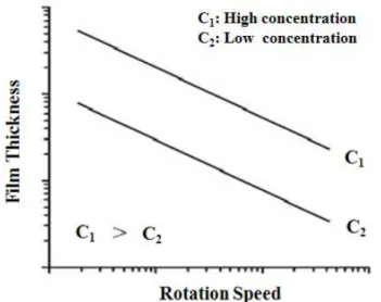
3.2.3: Variation of film thickness against rotational speed with solution
concentration..………...33
3.3.1: U-4100 Spectrophotometer………34
3.3.2: Configuration coordinate diagram for a broad band emission. An assumption is made on an offset between the parabolas of the ground
state and excited state……….………...36
3.3.3: (a) Diagram outlining the internal components of a basic TEM system (image provided by Gringer) (b) High resolution TEM images of Pt
nanocrystals………...39
3.3.4: FESEM JEOL - JSM-6700F………...41
3.3.5: AFM images of the generated surface on Corning 7740 glass after etching in HF (left figure) and HF/HCl 10:1 (right figure) for different
roughness.……...………...42
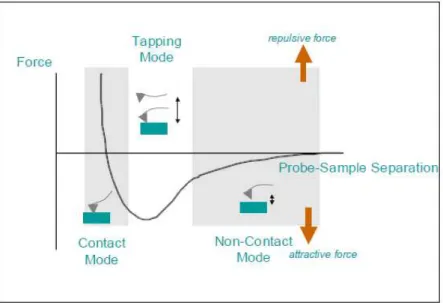
3.3.6: Plot of force as a function of the probe-sample separation (Robert A.
Wilson et al.)….………..………...43
4.1.1: An illustration of core-shell quantum dots……….44
4.1.2: The left shaded bottle with QDs reveals the original color but the right uncovered one shows a different blue-shifted color after 3 months of
storage...……….………45
4.1.3: Emission spectra at different illumination times via a spectrally resolved time trace of CdSe/ZnS QD in ambient air (excitation at 468 nm via
x
4.1.4: Flow chart of the hybrid PMMA/QDs films…………..………48
4.1.5: Illustration of the spin coating process for the fabrication of hybrid
PMMA/QDs films………..………...48
4.1.6: TEM images of CdSe/ZnS QDs……….49
4.2.1: Transmittance spectrum of CdSe/ZnS QDs for three weight ratio percen-
tages……….………..50
4.2.2: Absorption spectrum of CdSe/ZnS QDs with weight ratio percentages of
4.2 %, 8.3 % and 16.6 %……….………..51
4.2.3: First absorption peak of 4.2% CdSe/ZnS QDs fitted by a Gaussian
curve………..52
4.2.4: First absorption peak of 8.3% CdSe/ZnS QDs fitted by a Gaussian
curve………..52
4.2.5: First absorption peak of 16.6% CdSe/ZnS QDs fitted by a Gaussian
curve………..53
4.2.6: Transmittance spectrum of CdSe/ZnS QDs measured at wavelengths
ranging from 256 nm to 700 nm……….………...54
4.2.7: Reflectance spectrum of 16.6 % CdSe/ZnS QDs measured at
wavelengths ranging from 256 nm to 700 nm………...………55
4.2.8: Absorption spectrum of 16.6 % CdSe/ZnS QDs measured at
wavelengths ranging from 256 nm to 700 nm………...55
4.2.9: Photoluminescence (solid) and absorption (dotted) spectra of CdSe/ZnS
QD in chloroform provided from PlasmaChem GmbH………….…...57
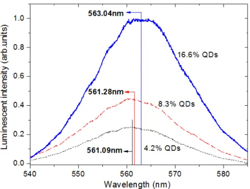
4.2.10: Luminescence of weight ratio percentage 4.2 % CdSe/ZnS QDs……57
xi
4.2.12: Luminescence of weight ratio percentage 16.6 % CdSe/ZnS QDs…..59
4.2.13: Luminescence measurements of PMMA layers with different weight
ratio percentage CdSe/ZnS QDs: 4.2 %, 8.3 % and 16.6 %……...….60
4.2.14: Different weight ratio percentage QDs continuously excited by laser
for 60 seconds showing an enhancement of emission intensity……..61
4.2.15: Weight ratio percentage 4.2% QDs continuously excited by a laser for 1910 seconds (sec) showing an enhancement of emission
intensity………..……….62
4.2.16: Weight ratio percentage 8.3% QDs continuously excited by a laser for
1910 seconds showing an enhancement of emission intensity………..63
4.2.17: Weight ratio percentage (w.r.) 16.6% QDs continuously excited by a laser for 1910 seconds showing an enhancement of emission
intensity……….63
4.2.18: Emission peaks blue shifted from the first time emission peak caused
by continuous laser excitation………...65
4.2.19: Emission peaks FWHM increasing from the first time emission peak
caused by continuous laser excitation………...65
4.2.20: A coupling effect occurring between quantum dots…………...……..66
4.2.21: The energy transference induced by the coupling effect………..66
4.2.22: A 3 mW power laser excitation on w.r. 4.2% QDs induced a quick saturation and even a decay of emission intensity for 1910 seconds....68
4.2.23: A 3 mW power laser excitation on w.r. 4.2% QDs showing a quick
increase and a decay of emission intensity………68
4.2.24: A 3 mW power laser excitation on w.r. 8.3% QDs induced a quick satu-
xii
4.2.25: A 3 mW power laser excitation on w.r. 8.3% QDs showing the quick
increase and the decay of emission intensity……….69
4.2.26: The emission peak is blue shifted and FWHM is widened with laser
illumination time for w.r. 4.2 % QDs………71
4.2.27: Emission peak is blue shifted and FWHM is widened with laser
illumination times for w.r. 8.3 % QDs………...………71
4.3.1: AM1.5G spectrum showing the fraction that is currently absorbed by a thick silicon device and the additional regions of the spectrum that can
contribute towards up- and down-conversion………...72
4.3.2: Absorption and photoluminescence spectra of a PMMA layer containing
CdSe/ZnS QDs………..74
4.3.3: Illustration of solar cell device composed of CdSe/ZnS QDs frequency conversion layer (left figure) and TEM image of CdSe/ZnS QDs
distribution (right figure)………...74
4.3.4: Measured external quantum efficiencies of silicon solar cells with and without a glass coated with a PMMA layer contained CdSe/ZnS QDs.
In this last case, the EQE has been divided by T() of the QDs
layer………...76
4.3.5: EQE difference between original solar cell and that covered by the QDs layer showing the exciton features are related to different QDs
absorption peaks……..………..77
4.3.6: (a) Solar cell has a covered QDs layer for down-conversion frequency.(b)
Solar cell has QDs inclusion in its active layer……….78
4.3.7: Model used for FDTD calculations. CdSe nanoparticles of 3 nm in diameter are embedded into a P3HT/PCBM layer: (a) top view and (b)
side view………78
4.3.8: Electric field distributions in the X-Y plane for two incident wave- lengths and two different distances between the nanoparticles (NPs)...79
xiii
4.3.9: Electric field distributions are in the X-Z plane for distance of 1 nm
between the NPs for two incident wavelengths: (a) 0.4 m (b) 1 m...80
4.3.10: Electric field profiles in X-direction for a distance of 1 nm between the
NPs and for two incident wavelengths: (a) 0.4 m (b) 1 m…………80
5.1.1: A polymer transition from glass to rubber type………..82
5.1.2: Heating temperature (T) effects on imprinted pattern: A tested on a
PMMA layer………..83
5.1.3: Transferred pattern showed a colorful appearance on a PMMA layer...84
5.1.4: Tunable He-Ne laser………...85
5.1.5: Periodic structure with good transfer. Left: Tunable laser at emission wavelength of 633 nm. Right: Tunable laser at emission wavelength of
594 nm………...85
5.1.6: Periodic structure with bad transfer. Left: Tunable laser at emission wavelength of 633 nm. Right: Tunable laser at emission wavelength of
594 nm………...86
5.1.7: An illustration of the chromatic confocal system (From the STIL SA).88
5.1.8: A 2-D mapping of the periodically imprinted structure of PMMA……88
5.2.1: Nanoimprinting method applied in order to obtain nanostructured polymer films: (a) sketch of a silicon mold with a periodic structure and (d) is its cross section; (b) principle of the imprinting process via thermal imprinting lithography (NIL) and (e) in cross section; (c) shows the expected nanostructured hybrid polymer with its cross section
(f)……….………..90
5.2.2: Patterned silicon mold with its periodic structure………..91
5.2.3: Nanostructured hybrid thin film with QDs via nanoimprint using a mold
xiv
5.3.1: Calculated first order diffraction angle vs. wavelength for a grating
period of 1.6 m. As the emission wavelength of the QDs of 560 nm,
the diffraction angle is expected to be 20.5……..………...93
5.3.2: (a) Cross section of simulation structure; (b) top view of simulation
structure……….94
5.3.3: Left: Cross section of the structure. Right: Electric field simulation at
560 nm………...………95
5.3.4: Left: Top view of the structure. Right: Electric field simulation from the
dashed region……….95
5.3.5: An illustration of far field projection on hemisphere curve…………...97
5.3.6: Far field simulation of diffraction pattern distribution with emission
wavelength of 560 nm………...97
5.3.7: Left: kz direction plane wave emission source. Right: Random dipoles
emission sources at wavelength of 560 nm………...98
5.3.8: Left: Cross section of the structure. Right: Electric field simulation with
random dipoles emission at wavelength of 560 nm………..99
5.3.9: Left: Simulation region located just above the structure. Right: Electric
field simulation from random dipoles emission………99
5.3.10: Electric field profile from distance 1 m above the top cylinder
structure………...100
5.3.11: Left: Top view of the structure. Right: Electric field simulation with
random dipoles emission from the selected region……….101
5.3.12: Far field simulation of diffraction pattern distribution from random
xv
List of tables
1. Center wavelengths of first absorption peaks and related Gaussian curve fittings obtained with PMMA layers containing w.r. 4.2%, w.r. 8.3% and
w.r. 16.6% QDs………..………....53
2. Center wavelengths, shifting of the wavelength from 560 nm and FWHM of the photoluminescence spectra obtained with PMMA layers
1
Chapter 1: Introduction
In recent years, nano-objects have attracted many studies. A nanostructured
material can be defined as a system with patterns in the range of 1-100 nm. In
fact, different scales of natural materials surrounding us, from atoms and
molecules to crystals and bulk components, have their own intrinsic
nanostructure. Thanks to tremendous progress in nanotechnologies, optical
materials can also be artificially structured at different nanometer-scales [1].
Up till now, nanotechnology has primarily been concerned with the physical,
chemical, biological and engineering fields including the realization of artificial
structures at the nanometer scale level. Among the multitude of nanomaterials
created, nanocrystals (NCs) are one of the key elements whose design and
function can be modified, tailoring their fundamentally chemical and physical
properties. A particular class of NCs which is quite popular and today represents
the most fascinating and potentially revolutionary inorganic semiconductor
material, is the family of colloidal quantum dots [2]. In QDs electrons, holes and
excitons can be in strong quantum confinement when the dimensions of the
material are smaller than the Bohr radius [3]. If excitons are strongly confined,
then remarkable and novel optical and electrical properties are obtained.
Quantum dots are also referred to as “nanocrystals” and the colloidal
definitions reveal their chemical origin. In fact, chemical synthesis currently
represents the most effective way to obtain high quality (in terms of size control,
narrow size distribution, good crystalline structure and high optical
performances) nano-objects on the gram scale [2]. Thus, they can be handled as
2
opto-electronic devices (lasers, light emitting diodes or solar cells) [4, 5], as well
as in biological applications (in vivo imaging or labeled molecular) [6-9].
This dissertation focuses mainly on the characterization of quantum dots and
their applications in nanocomposite thin films. This research is based on the
cooperation between the Department of Optics and Photonics, National Central
University in Taiwan and the OPTO-PV team, Institut Matériaux
Microélectronique Nanosciences de Provence (IM2NP), Aix
Marseille University in France. The whole work is organized into three principal
subjects. The first subject discussed the novel optical behavior of
nanocomposited PMMA thin films containing semiconductor quantum dots. The
second subject is focused on the control of light propagation by imprinting
periodic structures in these hybrid polymer/ QDs thin films. The third subject
considers the effects of these ideas and techniques applied to solar cells.
In the chapter on hybrid organic thin films/ quantum dots, we present the
characteristics of quantum dots embedded into PMMA thin films. The
experiment was performed by means of the proper composition of solutions and
the spin coating technique in order to deposit thin films. From their optical
properties, strong excitonic features caused by quantum confinement were
observed. Particularly in the photoluminescence analysis, a manifestly strong
peak with narrow width is obtained and evidence of the coupling effect between
quantum dots is also discovered. Moreover, we demonstrate the QDs properties
of the down-conversion frequency which can be directly applied to solar cells.
Through the external quantum efficiency analysis we show that photons
converted from UV to visible light by the QDs are absorbed by solar cells.
Once a strong photoluminescence is obtained, it becomes more attractive and
3
spatial distribution. For this purpose, we present our structuring method based
on imprint techniques. Thanks to the transition temperature of PMMA,
thermally assisted nanoimprints can be applied to transfer the structure from a
silicon mold to the hybrid PMMA/QDs layers. After theoretical and
experimental analysis, the periodic structure is well defined showing significant
2D-grating properties. By means of electric field simulation, a controllable QDs
4
Chapter 2: Nanomaterial evolution and nanoimprint
technique
2.1 Development of nanostructured materials
For nanostructured materials, especially nanocrystals, we now provide a brief
overview of the main studies regarding them carried out until now. Thus the
section is organized from nanostructures existing in nature, artificial
nanostructured materials and the new generation. The main focus in our study is
on nanocrystal materials, because of early developments which have lead to a lot
of useful applications. Furthermore the new generation nanocrystals of a
core-shell type are also considered and compared with single core nanocrystals.
When changing over from bulk to nanocrystal semiconductors both the
electronic and optical properties are affected. In Figure 2.1.1, the density of
states is varied from a bulk to a 0D (dot) semiconductor with a change from
continuous to discrete energy states induced by confinement effects [3]. The 1D
and 0D structures are analogous to quantum wires and quantum dots [2, 3].
Figure 2.1.1: The “Density of States” (DOS) function evolves from a bulk (3D solid) to a 2D, 1D and 0D system with varying degrees of confinement. [2, 3]
5
2.1.1 Nanostructures in nature:
Nanotechnology has been quickly developing during these last few decades.
However, we are already actually surrounded by many amazing nano-materials
in nature. The most typical one is the “lotus” noted for its water-repellent and
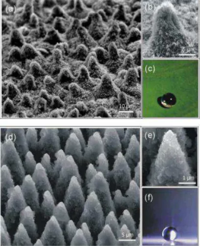
self-cleaning surfaces. Figures 2.1.2 (a) and (b) who a lotus leaf surface covered
by micrometer-sized papillae decorated with nanometer branch-like protrusions
[10]. The roughness of papillae reduces the area of contact between the surface
and a liquid drop. This ideal structure has inspired scientists to “imitate” it for
fabricating artificial self-cleaning surfaces as in Figure 2.1.2 (d) and (e) [10].
Figure 2.1.2: (a) SEM image of the surface of a lotus leaf and (b) a higher magnification with hierarchical structures clearly resolved. (c) A water drop on the surface of the lotus leaf attains
a nearly spherical shape. (d) SEM image of the artificial laser- structured silanized silicon surface and (e) a higher magnification showing the dual length-scale roughness. (f) A water
6
It is however not only plants like the lotus, but also many insects and animals
have their own nanostructure, for example beetles, sea mouse and butterflies
[11]. Due to genetic evolution, their structures which are built up in the
nano-sized range are naturally created by their molecular precursors. Another
example is our own body, comprised of a systematic composition of many
nanostructured materials such as the structure of DNA, a nanostructure existing
within the nucleus of a cell which stores information on evolution.
As shown in Figure 2.1.3 (a) and (b), the natural structure of butterfly wings
is quite interesting. Most of the butterflies of the Papilio species present a
common bulk and surface structure. The upper membrane is constituted of a
multilayered air/chitin film [12]. An important property of the super
hydrophobic surface of butterfly wings is found with a contact angle of about
160 [12] which is close to that of the lotus. In addition, the natural structure of butterfly wings can be replicated as can be seen in Figure 2.1.3 (c) and (d).
Figure 2.1.3: SEM images of the butterfly wing (a) and (b), the replicated surface (c) and (d). Angle of view: 45.The scale bar corresponds to 50 µm on (a),(c) and to 5 µm on (b),(d). [12]
7
2.1.2 Artificially nanostructured materials: semiconductor quantum dots
At the beginning of the 80s, a novel size effect induced by nanocrystals of
very small size was discovered by A.L. Ekimov et al. [13]. In this paper, the
exciton absorption spectrum of CuCl crystals grown in a dielectric matrix has
been studied. The crystal size could be controlled from several tens of angstroms
to hundreds of angstroms. With size variations, an absorption shift (of up to 0.1
eV) could be attributed to a quantum size effect [13]. In 1988, M.A. Reed et al.
investigated the electronic transport through a three-dimensionally confined
semiconductor quantum structure [14]. They showed that the fine structure
observed in resonant tunneling through the dot corresponds to a discrete density
of states of a zero-dimensional system. This zero-dimensional system was also
named for the first time as "quantum dots" [14].
General synthesis and processing of monodispersed nanocrystals [15]:
In the general synthesis of monodispersed nanocrystals, classic studies by La
Mer et al. have shown that the production of monodisperse colloids requires a
temporally discrete nucleation event followed by slower controlled growth on
the existing nuclei as shown in Figure 2.1.4 [16]. It is necessary to raise the
precursor concentration above the nucleation threshold via rapid addition of
reagents to the reaction vessel. The result of a short nucleation burst can
partially relieve the super-saturation. If the consumption of feedstock by the
growing colloidal NCs is not exceeded by the rate of precursor addition to the
solution, no new nuclei is formed. Because the growth of any type of NC is
similar to all others, the initial size distribution is mainly determined by the time
over which the nuclei are formed and begin to grow. Monodispersed NCs with
8
Figure 2.1.5 shows high resolution TEM observations of the size and shape of
CdSe NCs. This image indicates a nearly spherical shape with a size of around
3.9 nm that was clearly produced. [15, 17].
Figure 2.1.4: (A) Depiction of the stages of nucleation and growth for the preparation of monodispersed NCs in the framework of the La Mer model. As NCs grow with time, a size series of NCs may be isolated by periodically removing aliquots from the reaction vessel. (B) Representation of the simple synthetic apparatus employed in the preparation of monodisperse NC samples. [15, 16]
Figure 2.1.5: Collection of high resolution TEM images for typical NC materials such as (A) <100>-oriented CdSe (scale bar =15 Å), (B) <001>-oriented CdSe (scale bar =15 Å). [15, 17]
9
General energy bandgap blue shift with size:
Many types of semiconductor NCs (or QDs) have been developed during the
few decades including CdSe, CdS, CdTe and PbS compounds [18, 19]. Their
energy bandgaps are very different, making possibly numerous applications.
One of the most attractive characteristics of these semiconductor QDs is the
size-dependent band gap which was caused by quantum confinement effect [3]
which can be theoretically understood by solving the Schrödinger equation, for
example, a simple case of electrons in 1-dimension [20]. Via this confinement
effect, the essential bulk energy bandgap can be significantly shifted to a higher
photon energy (blue-shift phenomenon) with its decreasing size [21]. As shown
in Figure 2.1.6, both CdSe and PbS nanocrystals revealed a blue-shifted
absorption spectra with reduced size. The same shift is also obtained on the
luminescent spectrum, as shown in Figure 2.1.7.
Figure 2.1.6: (a) Size tuning of CdSe nanocrystal absorption spectra spanning the visible spectral region. (b) Size tuning of PbS nanocrystal absorption spectra spanning the near- infrared (NIR) spectral region. (c) Transmission electron microscope (TEM) images of different PbS nanocrystal samples with average sizes ranging from 2.3 to 5.5 nm. [18, 19]
10
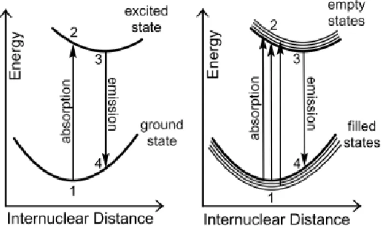
A red-shift can be observed between the absorption and emission of QDs.
Some possible explanations are illustrated in Figure 2.1.8 [22]. This figure
reveals different possibilities linked to the electronic energy transition due to the
splitting of the discrete energy levels caused by quantum confinement in the
semiconductor nanoparticles [3].
Figure 2.1.7: Colloidal suspensions of CdSe quantum dots of increasing size from left (approximately 1.8 nm diameter) to right (approximately 4.0 nm in diameter). Bottom: Samples viewed in ambient light vary in color from green–yellow to orange–red. Top: The same samples viewed under long-wave ultraviolet illumination vary in color from blue to yellow. [22]
Figure 2.1.8: Relationship between absorption and emission energies for discrete molecules (left) and for semiconductor nanoparticles (right). When a photon is absorbed thereby exciting an electron from the ground state (1) to an excited state (2) the bond order decreases and the atoms relax to a longer internuclear distance (3) before the emission of a photon (4) and relaxation to the ground state (1). In semicond uctor nanoparticles the process is the same (steps 1–4) but there are more possibilities for the energy of the electron under excitation from a photon to match an electronic energy transition. [22]
11
2.1.3 New generation of semiconductor quantum dots:
One of the primary aims in modern materials is the design of new
nanomaterials that exhibit novel properties to be utilized in various applications.
With similar aims, colloidal techniques have the potential for developing elegant
extensions of the synthetic NCs. These novel NCs involve the fabrication of
hybrid NCs in which domains made from different materials can be assembled
together in a single nano-object. These nanostructures would merge the
properties of the individual materials, with new properties being likely to arise
from their combination. In the synthesis of NCs made of more than one material,
the formation of a large interface between the two materials is also frequently
observed when the lattice constants of the two components do not differ
significantly from each other [23].
Semiconductor core and core-shell quantum dots:
Generally the semiconductor quantum dots exhibit high luminescence
emissions. This high efficiency of light emission is largely due to the strong
overlap between the electron and hole wave functions in the confined quantum
structure, whereas the exciton in bulk semiconductors is not confined in space
and can rapidly dissociate, increasing the probability of nonradiative relaxation
events associated with crystalline defects and charge carrier traps on the crystal
surfaces [24]. However, there still exists a major source of nonradiative decay
from the surface trap states, represented by unsaturated bonds on the surface
[25]. Thus, it is important to have another type, namely core–shell nanocrystals,
for passivating and further enhancing the luminescence from the core particles.
Normally the CdSe core with a low bandgap can be covered by a wider bandgap
12
Figure 2.1.9: The band gaps and their relative alignment for selected semiconductor materials with the band offsets. The numbers in the bars indicate the width of the bulk band gap in electron volt. [26]
Figure 2.1.10: (a) Fluorescence spectra of one type of CdSe nanocrystals overcoated with shells of ZnS of different thicknesses. The CdSe cores have a diameter of 4.2 10% nm and the shells have a thickness of (a) 0, (b) 0.65, (c) 1.3, (d) 2.6, and (e) 5.3 monolayers of ZnS. In addition to the variations of the quantum yield (see inset), one can also observe a red shift and a broadening of the spectra with an increasing shell thickness. (b) Radial probability density of the electron and the hole for the lowest energy states for CdSe cores and CdSe/ZnS core–shells. Due to the lower step in the potential at the surface of the CdSe section in the case core–shell nanocrystals, the probability density in the ZnS section is increased when compared to the respective volume in the case of the bare CdSe cores. This leads to an efficient increase of the confinement volume and thus to a slight red shift of the optical properties. [27, 28]
13
In Figure 2.1.10, the area under the wave function of both the electron and the
hole in the matrix surrounding the nanocrystal is decreased in the case of the
core–shell nanocrystals, and thus the probability of finding excitons in this area is also diminished. Therefore, the probability of an interaction between the
excitons and the host matrix is reduced as well [28].
Type I and type II semiconductor core-shell quantum dots:
The core-shell Type 1 QDs are described. The band edges of the core material
are localized in the band gap of the shell material. CdSe/ZnS is a typical case for
Type I. Moreover, in 2003, Bawendi and co-workers proposed a new type of
core-shell semiconductor heterostructure for which the conduction and valence
bands of the core and shell material are staggered, resulting in the segregation of
electrons and holes between the core and shell materials [29].
Figure 2.1.11: Alignment of the conduction and valence band edges for two types of hetero- structures. (a) Type I has a straddling configuration, whereas type II (b) is staggered. [30]
14
The goal in the formation of type II heterostructures is to generate a
considerable red shift in the optical properties [28]. As can be seen in Figure
2.1.11, the type II heterostructures can induce electrons to be mostly confined in
the core material and cause holes to be mostly confined to the shell material, for
example, CdSe/ZnTe core-shell QDs [29]. Thus the localized electrons/holes in
different sections can obtain a longer exciton lifetime via reduced overlaps [28].
Semiconductor nanorods and other unique shapes:
Other unique structures were studied by Milliron DJ, Hughes SM, et al.
Figure 2.1.12 shows inorganically coupled colloidal QDs and rods which can be
connected epitaxially at branched and linear junctions within single NCs [31].
Figure 2.1.12: Nanocrystal heterostructures. Extended rods (a) were formed by first growing CdS nanorods (b), and then adding CdSe extensions to each end. Branched rods (e) result from nucleation of CdTe on either end of CdSe nanorods (f ). A CdTe zinc-blende region at one end creates the branch point. CdSe tetrapods (c, g) comprise a zinc-blende core and four wurtzite arms. Extending each arm linearly with CdTe yields extended tetrapods (d). Branched tetrapods (h) result from nucleation of CdTe zinc-blende branch points on the end of each arm. The model sequences illustrate the growth processes. In each case, the first generation is shown in gray and the second in yellow, while red and blue parts indicate the unique crystal faces of the wurtzite structure. [31]
15
2.2 Development of nanocomposite thin films
Regarding the nanocomposite thin films, they can be treated as films
composed of different distinct phases where a characteristic length scale is in the
order of a few nanometers. Generally two distinct phases are mostly defined in
nanocomposite thin films. Due to the unique nanostructures, these artificial new
materials are expected to display optical properties totally different from bulk
composites ones. Several types of nanocomposite thin films have been
considered in many applications such as multilayered thin films and granular
nanocrystal thin films. Conventionally the optical properties of the former type
of film gained considerable attention and there are only a few studies on the
latter type [32]. For the former type, the multilayers are composed of two or
more different materials with different refractive indices. Many types of
spectrum filters can be obtained such as high/low pass filters and narrow-band
pass filters, anti-reflection (AR) coating, and thermal mirrors for improving the
optical system and optoelectronic device. For example, there are already many
applications which use AR coating in displays and solar cells.
With more and more developments and improvements in nanotechnology, the
granular nanocrystal thin films can achieve more and more sophisticated
compositions, for example, dielectric/granular metal, dielectric/embedded
semiconductor crystals, polymer/ embedded semiconductor crystals, and so on.
Different composite thin films belong to their own function. Take granular metal
films as an example. They are composed of a thin film ceramic matrix
embedded with metal granules of diameters as small as a few nanometers, and
exhibit novel behavior in terms of their hardness and apparent elastic behavior
16
2.2.1 Dielectric material contains nanocrystals:
In many types of nanocrystals/dielectric nanocomposite layers, the
silica-based nanocomposites are considered one of the potential systems for
quantum confinement in semiconductive nanocrystallites in order to have better
control of their shape and properties [33]. These embedded compositions can be
considered as metal or semiconductor nanocrystals.
Metal nanocrystals/dielectric nanocomposites: their optical properties have
attracted numerous studies because of the unique electronic properties and
surface-enhanced spectroscopic applications compared to the bulk material [34,
35]. Many studies have been reported the effect of reducing metal particle size
on the optical process in these films. When such a metal–dielectric
nanocomposite is excited by light, photons are coupled to the metal–dielectric
interface, causing an induced charged density oscillation and showing a strong
absorption maximum, called the surface plasmon resonance [36]. The resonance
frequency is influenced by several factors, e.g., the size and shape of the
nanoparticles and also their surrounding environment [37]. In [36], silver
particles embedded in the silica nanocomposite thin films were prepared by high
pressure DC sputtering technique. These increase in substrate temperature easily
causing a variation in the size and shape of the nanoparticles. Films containing a
distribution of particle sizes and shapes lead to an inhomogeneously broadened
and asymmetrical surface plasmon resonance in the optical absorption spectra.
They found that the size and shape distribution of metal nanoparticles has a
profound effect on the optical absorbance spectra.
Semiconductor nanocrystals/dielectric nanocomposites: the wide bandgap
material ZnO has attracted much research attention due to its desirable physical
17
temperature [38] which can provide efficient excitonic emission at room
temperature. Because ZnO emits a broad luminescence emission in the
green–yellow region, this property renders it as a potential material for blue- or
white-light emitting devices [39]. There are many methods for making an
emitting ZnO/SiO2 nanocomposite thin film, such as the sol–gel [38], molecular
capping [40] and also the sputtering method which can be employed [39]. Figure
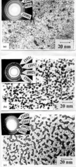
2.1.1 clearly shows crystallized ZnO NCs embedded in a silica matrix[33].
Figure 2.2.1: TEM micrographs and electron diffraction patterns of three representative ZnO/SiO2 nanocomposite films annealed in air for 10
18
2.2.2 Organic polymer containing inorganic nanocrystals:
Organic polymer/inorganic hybrid materials are promising candidates that
have attracted considerable attention due to their variable physical and chemical
properties for materials including nanoparticles [41]. Incorporating inorganic
nanoparticles into a polymer matrix is most straightforward and common
method for fabricating such hybrid materials. There have been several
publications on hybrid materials with their enhanced electrical, mechanical and
optical properties.
To obtain tunable electrical properties with nanocomposite material, it
can be achieved through hybrid polymer/metal particles. In [41], silver is
incorporated into polytetrafluoroethylene (PTFE). They found that near the
percolation threshold an expected sharp change in the resistivity from 107
(polymer-like material) to 10-3 for a metal-like material, when increasing the
silver content in the polymer. In this case, a significant change in resistivity of
several orders of magnitude occurs with just a small percentage point change in
the metal amount, as clearly shown in Figure 2.2.2.
Figure 2.2.2: Change of the electrical resistivity with an increase in filling factor for Ag/PTFE nanocomposite films. [41]
19
To obtain tunable optical properties with nanocomposite material,
inorganic nanoparticles can be embedded in a polymer matrix to form a high
refractive index nanocomposite [42]. For example, incorporating PbS
nanoparticles into gelatin or poly(ethylene oxide) has been reported [43, 44].
High refractive index nanocomposites have also attracted considerable interest
in light emitting diodes (LEDs) encapsulation [45]. The light extraction
efficiency will be greatly enhanced due to internal reflection phenomena
occurring at the interface between the light emitting semiconductor layer and the
resin [42]. On the other hand, titanium oxide (TiO2, titania) is well-known as an
inorganic material having a high refractive index, ~2.45 (anatase) and ~2.70
(rutile) [46]. Thus it can be another potentially promising incorporated material
for the polymer matrix to achieve hybrid layers with a high refractive index.
To obtain tunable optical properties in the nanocomposite material such as
absorption spectrum and luminescent emission wavelength, the change of
nanoparticle size is a direct solution because of the quantum confinement effect.
Typical absorption and luminescence spectra of samples with different ZnO QD
sizes separately estimated to be 12, 7.4, 6.5, 5.3, 4.2 and 3.5 nm are shown in
Figure 2.2.3 [47]. The UV emissions represent the relaxed state of the excitons
near the band edge in ZnO QDs [47]. In general, quantum confinement shifts the
energy levels by generating a blue shift in the transition energy while decreasing
the particle size. Thus with the nanocomposite material, we can not only control
the level of spectral blue shifts by tuning the particle size, but we can also
modify the spectral intensity from the particle doping ratio. Figure 2.2.4 [4],
ZnO-QDs embedded in a transparent epoxy used for the encapsulation of UV
light-based white light emitting dioxides (UV-WLED) lamps shows an example
20
Figure 2.2.3: PL (solid line) and absorption (dashed line) spectra near the band edge of various sized ZnO QDs. [47]
Figure 2.2.4: Fluorescence emission spectra of pure epoxy and ZnO QDs/epoxy nanocompo- sites excited at 370 nm. The inset shows the photographs of the UV-WLED lamps (370 nm)
encapsulated with the pure transparent epo xy (left) and the ZnO QDs/epoxy nanocomposite (right) containing the 4 wt % ZnO QDs content. [4]
21
2.3 Historic development of nanoimprint lithography
Nanoimprint lithography (NIL) is a novel method to fabricate micron to
nanometer scale patterns with high-throughput and low-cost [48]. Originally the
NIL technique was developed due to the high cost and limited resolution of
optical lithography [49]. Scanning electron beam lithography can reach 10 nm
resolutions. However, mass production of sub-50 nm structures seems
economically impractical due to inherent low throughput in a serial processing
tool [50, 51]. X-ray lithography can have a high throughput with demonstrated
50 nm resolutions, but the cost of X-ray lithography is much higher [52]. For the
above reasons, the nanoimprint lithography technique was first proposed by
Stephen Y. Chou and his students in 1995 to provide researchers with the means
they needed to have a high resolution patterning technique with a structural size
below 0.1 m [51].
The term NIL initially referred to a hot embossing lithography (HEL) process,
and was also used as a synonym for thermal nanoimprint lithography [51].
However, it now has an extended meaning which includes not only the two
fundamental types (Thermal NIL and UV-based nanoimprint lithography,
UV-NIL), but also many different variations subsequently developed, such as the
roll imprint process, laser-assisted direct imprint, reverse imprint, etc [49]. The
former two general methods will be discussed in detail in the following sections.
In the applicable fields the NIL technique can create resist patterns, imprint
functional device structures and even on large-areas from micron to nanometer
scale. Thus, this leads to a wide range of applications in biotechnology [53],
electronics (LED, OLED, flexible display), photonics, data storage (Hard Disk
Drive) and so on [49, 54]. NIL has great potential for commercial prospects and
22
2.3.1 Thermal nanoimprint lithography:
In this section, we discuss the mechanisms of thermal NIL and give examples
of the requirements for commonly used plastic materials. In the mechanism of
thermal NIL, it is important to make sure that the temperature of the material
increases to around the glass transition temperature (Tg), so that the polymer
reaches a typical viscoelastic behavior. In these states, the polymer becomes soft
enough to be imprinted. When the temperature keeps rising above the melting
temperature (Tm), the polymer turns into a viscous liquid and the polymer starts
to flow [55]. Normally the temperature of thermal NIL is operated between Tg
and Tm with a proper casting high pressure. There are two requirements for the
thermal NIL process that can be met simultaneously via increasing the
temperature above the Tg of the polymer, so that both Young’s modulus and the
viscosity will drop by several orders of magnitude compared to their respective
values at room temperature (Young’s modulus for glassy polymers just below Tg
is approximately constant over a wide range of polymers, at ~3×10⁹ Pa) [54].
Of the thermal plastic polymers, polymethylmethacrylate (PMMA) can be a
good candidate. There are several reasons were chosen for imprinting. First, the
PMMA polymer does not adhere well to the SiO2/Si mold due to its hydrophobic
surface. Thus it can provide good mold releas ing properties which are an
essential factor for fabricating all nano-scale features. Second, the shrinkage of
the PMMA polymer is less than 0.5% when encountering large changes in
heating temperature and casting pressure [51]. This means that the transferred
patterns can be stably maintained with little deformation process. An example is
shown in Figure 2.3.1 presenting 10 m circles replicated in a PMMA layer via
the NIL technique, revealing the clear transfer of patterns with a specific depth
23
Figure 2.3.1: AFM images of 10 m circles replicated in a PMMA layer by the NIL technique with an imprint force of 1000 N. [56]
The formation of a silicon mold can be accessed by another etching technique
like electron beam lithography. The mold can be comprised of gratings or
periodic cylinders that are quite characteristic of the transfer performance. Mold
engineering has been improved to meet more and more imprinting requirements.
Up to now, the mold can be of any desired morphology, where the focused ion
beam (FIB) technique is used to directly “carve out” the desired mold features.
Thus it is even possible to achieve 3D or gray-scale patterns that are generally
very difficult to fabricate, or would sometimes involve multiple steps including
other lithographic techniques to obtain. An example of such a structure
fabricated by FIB is shown in Figure 2.3.2. FIB may find many uses in
NIL-related applications with more complicated molds in the future [54].
24
2.3.2 UV-curable nanoimprint lithography:
Since 1995, nanoimprint lithography using the hot embossing technique (or
thermal NIL) has attracted much attention as an alternative method comparing to
conventional lithography. Another promising approach for UV-curable NIL was
established as an alternative to the thermal NIL and has now become another
common method just as important as the standard thermal NIL.
The UV-curable technique was first proposed by Haisma et al. in 1996 [57].
The thermal NIL process requires high temperatures and heavy pressures for the
nanoimprinting of thermoplastic materials. These could limit the throughput for
mass production via NIL techniques. On the other hand, the thermal expansion
mismatch between the mold and the substrate often presents an obstacle for
pattern overlay over large substrates. An alternative is to use liquid precursors
that can be cured by UV light at ambient temperatures. For such materials, the
low Young modulus and low viscosity requirements are naturally satisfied. The
low viscosity of the monomer fluid makes the imprinting process is less
sensitive to the effects of pattern density reported for NIL [54]. There are two
main polymer classes, which could be considered for the curing system:
acrylates (free-radical polymerization) and epoxy compounds (cationic
polymerization). The former shows higher polymerization reactivity and faster
curing rates than epoxy systems [58]. The curing reaction initiated by UV light
is shown in Figure 2.3.3.
Figure 2.3.3: Free-radical polymerisation of (meth)acrylates initiated by UV exposure (acrylates R=H, methacrylates R=CH3, Ri various functional groups). [58]
25
The process for UV-curable NIL is similar to thermal NIL techniques as
shown in Figure 2.3.4. The difference is that a UV-transparent mold is pressed
into a liquid resist layer and then hardened by exposure to UV-light at room
temperature. The defined patterns in the resist can then be transferred into the
underlying substrate via etching, much like the exposed and developed resist
layers in conventional lithographic technologies [59] . Compared to thermal NIL,
a low imprinting pressure is still needed for UV-curable NIL, which must be
sufficient to initiate lateral resist flow into the mold cavities. In addition the
casting pressure should be large enough to compress the air inside the cavity or
to dissolve it. If the environmental air pressure before the mold to sample
contact is lowered, the amount of air trapped inside the cavities is reduced
significantly and therefore the pressure required to initiate the lateral resist flow
is minimized [60].
26
Figure 2.3.5: SEM micrograph of a printed narrow channel transistor with a width of 80 nm and depth of 200 nm, transferred into silicon via UV-curable NIL. [59]
2.3.3 New material developments:
The rapid growth of NIL in recent years has led to the use of more and more
new materials as a nanoimprint resist for further development. In NIL, there can
be a reduction in precision caused by distortion of the imprinted structure or
stamp features due to the thermal cycle of heating followed by cooling. To
overcome these problems photo-curable monomers are used for polymerization
during the imprint process. However, this procedure generally utilizes
transparent quartz stamps that require a complicated fabrication process and thus
this becomes more expensive than the usual silicon stamps [61]. Therefore a
transparent and low-cost material in the UV range is required for photo-curable
methods. Several types of polymer systems have been investigated, for example,
one of the promising materials is a thermally curable Polydimethylsiloxane
(PDMS)-based liquid resist that can be imprinted with high precision,
UV-transparency and is very quickly for thermally crosslinked [54]. Until now,
PDMS has been used in many nano-lithography techniques, which are also
27
A combined UV-curable NIL technique, the Soft UV-Nanoimprint technique,
featuring transparent flexible molds and low viscosity UV-curable resist has
been developed, which enables the definition of high aspect nanostructures on
the wafer scale. PDMS is then used as a standard mold material due to its
favorable properties such as flexibility and UV-transparency [64].
On the other hand, the polymer, PDMS, has a much lower surface energy [65]
compared to the vast majority of resists used for thermal NIL methods such as
PMMA and polystyrene (PS). Thus this polymer can also directly replicate any
structure and even organic morphology like the lotus [12] because of its low
surface energy, flexibility and good chemical stability.
Figure 2.3.6: SEM images of a natural lotus leaf (a) and (b) and the replicated surface (c) and (d). Angle of view: 75 except for (b) 45.The scale bar correspond to 50 µm on (a), (c) and to
28
Chapter 3: Experimental framework and methods
3.1 Experimental framework
The important exitonic features in quantum dots motivated us to study the
quantum dots experimentally and to investigate their optical properties. An easy
method to study quantum dots experimentally is to disperse them in a solvent.
However, this liquid state is not convenient for application when compared to
thin films and devices. Therefore, we proposed embedding the QDs into
polymer thin films, such as PMMA, making hybrid layers of PMMA/QDs. The
choice of PMMA is made because of its transparency in the near UV and visible
range making it a potential candidate for the hosting matrix. Thanks to the
highly luminescent properties of these QDs, we then demonstrated this hybrid
layer/QDs can be applied to solar cells.
After obtaining the optical properties of hybrid thin films/QDs, we structured
these hybrid thin films/QDs into periodic structures in order to further control
the spatial distribution of the highly luminescence light of QDs. The structured
hybrid thin films were fabricated by the thermal nanoimprint method due to the
softened PMMA polymer above the transition temperature. After the optimized
nanoimprint, the transferred structural characterization of hybrid thin films and