HAL Id: lirmm-03168312
https://hal-lirmm.ccsd.cnrs.fr/lirmm-03168312
Submitted on 12 Mar 2021HAL is a multi-disciplinary open access archive for the deposit and dissemination of sci-entific research documents, whether they are pub-lished or not. The documents may come from teaching and research institutions in France or abroad, or from public or private research centers.
L’archive ouverte pluridisciplinaire HAL, est destinée au dépôt et à la diffusion de documents scientifiques de niveau recherche, publiés ou non, émanant des établissements d’enseignement et de recherche français ou étrangers, des laboratoires publics ou privés.
technologies
Abdoulaye Gamatié, Pierre-Yves Péneau, Gilles Sassatelli, Sophiane Senni,
Lionel Torres
To cite this version:
Abdoulaye Gamatié, Pierre-Yves Péneau, Gilles Sassatelli, Sophiane Senni, Lionel Torres. Deliverable D3.1 – Novel memory and communication technologies. [Research Report] LIRMM (UM, CNRS). 2016. �lirmm-03168312�
D3.1 – Novel memory and communication technologies
Version 2.0 (2016) Final Public Distribution Main contributors:A. Gamatié, P.-Y. Péneau, G. Sassatelli, S. Senni and L. Torres (LIRMM)
Project Partners: Cortus S.A.S, Inria, LIRMM
Every effort has been made to ensure that all statements and information contained herein are accurate, however the Continuum Project Partners accept no liability for any error or omission in the same.
Project Partner Contact Information
Cortus S.A.S Inria
Michael Chapman Erven Rohou
97 Rue de Freyr Inria Rennes - Bretagne Atlantique
Le Génésis Campus de Beaulieu
34000 Montpellier 35042 Rennes Cedex
France France
Tel: +33 430 967 000 Tel: +33 299 847 493
E-mail: [email protected] E-mail: [email protected] LIRMM Abdoulaye Gamatié Rue Ada 161 34392 Montpellier France Tel: +33 4 674 19828 E-mail: [email protected]
Table of Contents
1 Introduction 2
1.1 Some key numbers . . . 3
1.2 Goal of this study . . . 4
1.3 Outline of this deliverable . . . 5
2 Non-Volatile Memories 6 2.1 NVM historical development . . . 6
2.1.1 Magnetoresistance effect . . . 6
2.1.2 Magnetic tunnel junction . . . 7
2.2 A typical NVM: magnetic random access memory (MRAM) . . . 8
2.3 NVM modeling in practice . . . 11
2.3.1 Main evaluation tools . . . 11
2.3.2 An example of analysis based on NVSim tool . . . 12
2.4 Exploiting NVMs through compilation techniques . . . 13
2.4.1 Hybrid memory architectures . . . 13
2.4.2 NVM-specific compilation techniques . . . 14
2.5 Summary . . . 14
3 On-chip communication interconnects 15 3.1 Evolution of communication technologies . . . 15
3.2 Basic concepts on Network-on-Chip . . . 16
3.2.1 Topology . . . 17
3.2.2 Communication through packets . . . 18
3.2.3 Flow Control . . . 19 3.2.4 Routing strategy . . . 20 3.3 Examples of 2D Network-on-Chip . . . 21 3.3.1 Academic versions . . . 21 3.3.2 Industrial versions . . . 22 3.4 Towards 3D Network-on-Chip . . . 23 3.5 Performance metrics . . . 24 3.6 Simulation tools . . . 27 3.7 Summary . . . 28
4 Conclusions 30
Executive Summary
Memory and communication are major performance and energy bottlenecks in manycore architectures. They require a particular attention during system design in order to maximize the resulting energy-efficiency.
This deliverable surveys a number of existing candidate emerging memory and communication technologies, envisioned for the compute node architecture targeted by the CONTINUUM project. It first provides an overview of non-volatile memories by discussing in particular magnetic memories and their application in system memory hierarchy so as to improve the overall energy-efficiency. Then, it presents the main concepts related to on-chip communication interconnects, typically networks-on-chip (NoCs). Such infrastructures are more scalable than buses or crossbars when the considered architectures feature a high number of cores. The energy improvement studied in CONTINUUM relies on the integration of the previous innovative technologies with suitable heterogeneous manycore / multicore architectures.
1
Introduction
The evolution of architectures from single-core to manycore execution platforms, observed in the last decades, has seen a paradigm shift in processor architecture design. This concerned central elements such as CPU cores, memory architecture and communication interconnects.
(a) Simple monocore architecture (b) Monocore architecture with 3 cache levels
(c) Example of manycore architecture
Figure 1: Different architecture designs
In particular, advanced cache memory architectures including several levels have become mainstream in modern processors. Figure 1a illustrates a very basic design where a monolithic cache memory is inserted between the CPU core and the main memory in order to enable fast memory accesses. The communication is achieved via a classical bus. A state-of-the-art single-CPU system is shown in Figure 1b where several hierarchy levels are considered for a better data access locality. In this example, data and instruction caches are separated at L1 level, respectively into L1i and L1d caches. At L2 and L3 cache levels, they are considered indifferently. Finally, Figure 1c depicts a typical
manycore architecture generalizing the previous design where the communication interconnect can be a network-on-chip instead of a classical bus for scalability reason.
While current CPU cores can operate at high frequencies, the design of the memory and communication infrastructures appears as the most critical task for reaching an overall system energy-efficiency. In particular, selecting the most suitable technologies corresponding to these architecture components is central.
1.1
Some key numbers
In the current computing ecosystem, memory and communication have been key challenges for reach-ing energy-efficiency. Typically, with 22nm chip technology [60] movreach-ing 1 bit (for communication) on silicon consumes about 1 picojoule/mm (10−12J/mm), thus 1 milliwatt/mm at 1GHz frequency. Swapping a bit in a transistor only consumes 10−6pJ . Note that modern chips already comprise kilometers of wires, leading to many watts/cm2.
On the other hand, data exchanges are expected to represent the larger part of the activity in next decade distributed pervasive systems. Nowadays, the volume of data generated by the Internet of Things is already around 2.5 × 1018bytes/day.
Considering the aforementioned non negligible cost of moving bits with advanced chip technologies in terms of power, the scalability of power consumption corresponding to the data traffic foreseen in coming years will be very challenging. As a result, data management must be carefully considered by investigating suitable memory and communication infrastructures.
The decreasing size of the CMOS transistor enabled the fabrication of small devices running at high speed. Nevertheless, the counter-part of this technological evolution is significant power consumption of the resulting System-on-Chips due to the high density of their integrated components. Regarding the speed and power consumption metrics, memory and communications are key elements for upcoming efficient SoCs. Richard Sites, one of the fathers of computer architecture, noticed earlier in his article entitled "It’s the memory, Stupid!" [94]:
Across the industry, today’s chips are largely able to execute code faster than we can feed them with instructions and data... The real design action is in memory subsystems – caches, buses, bandwidth, and latency.
Regarding memory, Figure 2 illustrates the fact that memory systems consume more than 50% of the die area. As a results, a significant part of the consumed power is devoted to memory as reported in Figure 3. The current mainstream memory technology used for both cache memory and registers is SRAM thanks to the short data access latency it provides compared to other technologies. However, its potential prohibitive static energy due to the increase of the leakage current when decreasing the technology node is a major issue to energy-efficiency. In order to address this issue, embedding volatile memories in SoCs is among the most promising trends. Magnetic Random Access Memory (MRAM) is one promising non volatile candidate as it combines simultaneously high density and very low static power consumption while its performance is competitive compared to SRAM and DRAM.
Figure 2: SoC area repartition between logic and memory (from Semico Research Corporation [88])
On the other hand, Networks-on-Chip (NoCs) alleviate the bottleneck of usual buses and the prohibitive cost of crossbars in the context of a large number of cores by allowing parallel communications. With the limit of the single-core frequency scaling w.r.t. heat issue related to high power dissipation, parallel computing, e.g. well-illustrated by the proliferation multicore processors, has become the suitable paradigm. 3D-NoCs are typical emerging extensions of 2D NoCs for better communication efficiency.
Figure 3: SoC energy repartition between logic and memory (from ITRS [42])
1.2
Goal of this study
The current deliverable presents a survey of existing emerging memory and communication technolo-gies. The outcome of this survey will enable us to discuss the relevance of the target technologies and, to judiciously choose the most relevant ingredients for the design of compute node architecture expected in CONTINUUM project. We mainly focus on non-volatile memories and on-chip commu-nication interconnects. Among the surveyed technologies, a few will be evaluated during the project,
by covering both performance and power consumption improvement resulting from their integration in explored system designs.
1.3
Outline of this deliverable
In the remainder of this document, Section 2 presents an overview on non-volatile memories. It puts focus on magnetic memories, which currently appear as the most promising solutions among existing technologies. Then, Section 3 is devoted to a general presentation of on-chip communication interconnects, mainly networks-on-chip (NoCs). Finally, Section 4 gives concluding remarks and draws some interesting design directions to be considered in the design of the target compute node architecture so as to benefit from surveyed technologies.
2
Non-Volatile Memories
Non-volatile memories (NVMs) are parts of the emerging technologies foreseen for addressing the energy consumption issue in future technologies. A majority of current systems integrates volatile memories such as Static Random Access Memories (SRAM) and Dynamic Random Access memories (DRAM). Contrarily to those memories, NVMs potentially favor power consumption reduction by enabling a complete circuit power-down without losing data and logic states.
The survey presented in this section largely relies on [92]. We first introduce a few historical notes on the development of NVMs (Section 2.1) and we focus on magnetic random-access memory as one example (Section 2.2). The current exploitation of such technologies in practice via the main associated modeling and evaluation tools is discussed in Section 2.3. In addition, we present in Section 2.4 a few studies applying compilation techniques to NVM technologies as this will be a central question in the CONTINUUM project. Finally, a summary is provided in Section 2.5.
2.1
NVM historical development
While the electric charge of electrons has been used for decades to encode information in classical information processing, the usage of their spin offers another alternative to information encoding. This has been possible since the the discovery of spin-dependent electron transport phenomena in 80’s, which later on led to the Spintronics [101] information processing paradigm. Instead of considering the electric charge threshold of an electron for encoding 0 or 1 bit values, it is defined according to the spin orientation of the electron, i.e. “up” and “down”, w.r.t. a referential that can be a the magnetic orientation of a ferromagnetic film. Spintronics is expected to facilitate the development of non-volatile, denser and more energy-efficient devices in comparison to semiconductor devices.
2.1.1 Magnetoresistance effect
Applying a magnetic field to a material modifies its resistance due to the so-called Magnetoresistance (MR) effect. We distinguish three main MR effects, known as anisotropic magnetoresistance, giant magnetoresistance and tunneling magnetoresistance. In the sequel, these MR effects are briefly described.
1. Anisotropic magnetoresistance (AMR). William Thomson discovered in 1856 the AMR through experiments on iron and nickel when he observed a variation of the electrical resistance when an external magnetic field is applied. The electron scattering (i.e. electrons are deviated from their original trajectory) rate is affected depending on the direction of the field. When the magnetization is perpendicular to the current direction, the electron scattering is smaller, whereas when the magnetization is parallel to the current direction, the electron scattering is larger. In ferromagnetic materials, AMR affects the resistance in the order of a few percent. However, in the late 1970s, it was sufficient enough to successfully develop AMR sensors for replacing inductive sensors as the read head in hard drive.
2. Giant magnetoresistance (GMR). In the late of 1980’s, the GMR effect in structures alternat-ing ferromagnetic (FM) and non-magnetic (NM) layers has been discovered independently by two research groups led by Albert Fert and Peter Grünberg. The group of A. Fert investigated the MR of thirty to sixty stacked Fe/Cr structures and observed almost a factor of 2 between the resistivities at zero field and in the saturated state, respectively [10]. On the other hand, the group of P. Grünberg studied the MR of a simple Fe/Cr/Fe structure and noticed that an anti-parallel alignment of the magnetization of the Fe layers increases the electrical resistivity, much more than AMR effect. Similarly to AMR, the GMR effect relates to electron scattering.
3. Tunneling magnetoresistance (TMR). The TMR effect has been discovered first by Tedrow and Meservey in 1970 by observing that the tunneling electrons through junctions between very thin superconducting aluminum layers and ferromagnetic nickel layers is spin dependent [95]. In 1975, Michel Jullière studied the conductance of two ferromagnetic layers separated by a thin insulator [44]. TMR relies on the spin polarizations of the conduction electrons. In a parallel configuration of the material, electrons whose spin is parallel to the direction of the magnetization of the layers will tunnel through the barrier, whereas electrons whose is anti-parallel will be filtered. In an antianti-parallel configuration of the structure, both spin-up and spin-down electron flows are reduced, resulting in a large resistance. M. Jullière measured the conductance ratio, which is known today as the TMR ratio. In 1995, Terunobu Miyazaki and Nobuki Tezuka reported a TMR ratio of 2.7% at room temperature in a NiFe/Al2O3/Co structure [69]. In the same year, Moodera et al. observed the first giant TMR ratio of 11.8% in a Al2O3-based junction at room temperature [70]. Since 2004, junctions based on a Al2O3 barrier have reached a TMR ratio of 70%. However, the breakthrough regarding the TMR ratio will come with barriers based on the MgO. In 2001, Butler et al. and Mathon and Umersk theoretically predicted that a giant TMR ratio higher than 1000% could be obtained in fully epitaxial Fe(001)/MgO(001)/Fe(001) structure [19, 64]. In 2008, experimental TMR reached 600% at room temperature in a CoFeB/MgO/CoFeB junction [40]. The TMR effect have raised a great interest to design spintronic devices.
Figure 4 summarizes the evolution of the MR ratio and the associated device applications.
2.1.2 Magnetic tunnel junction
We introduce the magnetic tunnel junction (MTJ) as data storage unit. Basically, a magnetic random access memory (MRAM) bit is a MTJ consisting of two ferromagnetic layers separated by a thin insulating barrier. The information is stored as the magnetic orientation of one of the two layers, called the free layer (FL) or storage layer. The other layer, called the reference layer or fixed layer (RF), provides the fixed reference magnetic orientation required for reading and writing. The TMR effect causes MTJ resistance to depend significantly on the relative orientation of the two magnetic layers: the antiparallel state provides much larger resistance than the parallel state. It enables the magnetic state of the FL to be sensed thanks to a current flowing through the MTJ. Hence, stored information can be read.
Figure 4: Magnetoresistance ratio evolution [104]
2.2
A typical NVM: magnetic random access memory (MRAM)
A promising candidate for non-volatile SoCs is MRAM based on MTJ. Both academia and industry regard MRAM as a suitable technology to become a universal memory as it combines good scalability, low leakage, low access time and high density. A MRAM bit is an MTJ consisting of two ferromagnetic layers separated by a thin insulator. The information is stored as the magnetic orientation of one of the two layers, called the Free Layer (FL). The other layer, called the Reference Layer (RF), provides a fixed reference magnetic orientation required for reading and writing.
A conventional MRAM, as depicted in Figure 5, uses a simple way to program the MTJ where sufficient magnetic field is generated thanks to a combination of two current flows applied simultaneously through a row and a column of an MTJ array. Two problems arose with this method. First, large current is needed to generate sufficient magnetic field to reverse the magnetization of the FL. Second, this approach suffers from selectivity problem: some of the bits sharing the same row or column of the cell being programmed might be exposed to sufficient magnetic field and be switched unintentionally. This effect is one consequence of process variability. The magnetic field necessary to reverse the magnetization is not exactly the same for all the bits [51].
To switch the orientation of the FL, three methods have been proposed: Toggle [31], Spin Transfer Torque (STT) [47] and Thermally Assisted Switching (TAS) [84]. In addition to these methods, a voltage-controlled MTJ, also known as Magnetoelectric Random Access Memory (MeRAM), has been proposed in order to improve the scalability and to reduce the switching energy observed with STT-MRAM. Then, more recently the spin orbit torque (SOT) has been also developed as an alternative to STT-MRAM. We note that a great potential is expected MeRAM [93, 6], and SOT [34] technologies to reach similar performance as SRAM.
Figure 5: Conventional MRAM [7]
• The Toggle scheme uses a specific current pulse sequence through the conductive lines to generate a magnetic field to switch the magnetic orientation of the FL to its opposite direction. • STT-MRAM uses the spin transfer torque effect to switch magnetic orientation of the FL. A highly spin polarized current flowing through the MTJ induces a “torque” applied by the injected electron spins on the magnetization of the FL.
• TAS-MRAM adds an antiferromagnetic layer in order to block the FL magnetic orientation under a threshold temperature. To switch the bit cell, a select transistor provides a current flow to heat the MTJ above the blocking temperature enabling storage of new information thanks to application of a magnetic field. Recent studies show the promising features of MRAM technologies for improving cache memory energy consumption.
• MeRAM uses voltage rather instead of the current to reverse the magnetization of the FL thanks to the recently demonstrated voltage-controlled magnetic anisotropy effect (VCMA). The FL has a magnetic anisotropy that can be changed by voltage. Hence, voltage-induced switching of the magnetization can be performed modifying the magnetic anisotropy of the MTJ.
• SOT-MRAM uses a three-terminal structure (enabling bigger cell size) to separate the read and write paths contrary to STT-MRAM. It intrinsically separates the read and write paths and allows symmetrical switching current between the two states of the MTJ. Hence, read stability is improved, strongly reducing the possibility of a bit flip (the bit changes its state) during a read operation. Designers can optimize the read and write separately. As SOT-MRAM is a young technology compared to other MRAM technologies, further work is still needed to optimize the SOT-based MTJs.
Table 1 summarizes the differences between the above five MRAM technologies [92] and the more standard SRAM technology. Due to its voltage-controlled switching scheme, MeRAM requires a very low write current compared to the other technologies. Hence, very high scalability is expected. STT-MRAM and SOT-STT-MRAM show almost the same overall performance and are very good candidates to be part of the memory hierarchy of a Systems-on-Chip. The first test chips featuring STT-MRAM have been already developed. Among the five technologies, TAS-MRAM is the most reliable thanks to its MTJ structure which allows excellent thermal stability, hence a very good data retention.
T echnology Cell size (F 2 ) Access time Write curr ent Endurance Maturity Adv antages/Drawbacks read/write T oggle MRAM 50 35 ns / 35 ns > 30 mA 10 15 Commercialized (+) Maturity (-) High po wer [31 , 7 , 2 ] T AS-MRAM < 50 30 ns / 30 ns A fe w mA 10 15 T est chip (+) Reliability (-) Access time [1 , 84 , 85 ] [1 ] STT -MRAM < 50 2-20 ns / 2-20 ns 50 uA > 10 16 T est chip (+) Lo w po wer (-) Reliability [47 , 46 ] [76 , 41 , 77 ] MeRAM < 10 < 10 ns v ery lo w > 10 16 Prototype (+) Lo w po wer (-) Maturity [99 , 28 ] SO T -MRAM < 50 A fe w ns < 100 uA > 10 16 Prototype (+) Lo w po wer (-) Maturity [15 , 79 , 43 ] T able 1: MRAM technologies
2.3
NVM modeling in practice
There are a few existing NVM evaluation tools that enable to address their properties such as memory access latency and power/energy consumption. The next sections provide a short review with an illustration of the usage of one of these tools in a study.
2.3.1 Main evaluation tools
SPICE [73] is a general-purpose circuit simulation program that simulate the electrical performance of electronic circuits. This software will determine the quiescient operating point of the circuit, the time-domain response of the circuit, or the small-signal frequency-domain response of the circuit. SPICE contains models for common circuit component and is capable of simulating most electronic circuit. It supplies reasonable default values for circuit parameters that are not specified and performs a considerable amount of error-checking to insure that the circuit has been entered correctly. SPICE accepts as input a description of a circuit and provides several forms of accurate and detailed simulation, including small signal and time-domain transient solutions. The SPICE input syntax is a free-format style that does not require any specific formalism.
CACTI [72, 100] is an analytical model for the access and cycle times of on-chip direct-mapped and set-associative caches. It is an enhancement of a previous model [98] based on HSPICE1. The
CACTI cache access model takes in the following major parameters as input: cache capacity, cache block size (also known as cache line size), cache associativity, technology generation, number of ports, and number of independent banks (not sharing address and data lines). As output, it produces the cache configuration that minimizes delay (with a few exceptions), along with its power and area characteristics. CACTI models the delay/power/area of eight major cache components: decoder, wordline, bitline, senseamp, comparator, multiplexor, output driver, and inter-bank wires. The model gives estimates that are within 6% of Hspice result.
NVSim [27] is a circuit-level model for NVM performance, energy, and area estimations, which supports different NVM technologies including STT-MRAM, ReRAM, and PCRAM. In particular, it is a generalized extension of the PCRAMsim tool [26], which has been proposed for analyzing access times and power dissipation Phase-change random access memory (PCRAM), an emerging non volatile memory technology. NVSim uses the same modeling principles as CACTI, but starting from a new framework and adding specific features for NVM technologies. Like CACTI, NVSim also has the capability of modeling SRAM. NVSim is validated against several industry prototype chips within the error range of 30%. The main objectives of this tool is to facilitate the architecture-level NVM research by estimating the access time, access energy, and silicon area of NVM chips with a given organization and specific design options before fabrication. In [25], NVSim is combined with a gem5 model of heterogeneous multicore architectures [17, 18] to build a seamless evaluation flow for NVM-based design exploration (gem5 is a cycle-approximate architecture simulator [13]). This flow has been leveraged in [81] for assessing the impact of software loop optimizations on the energy-efficiency in systems with STT-MRAM caches.
Destiny [83] is a 3D design-space exploration tool for SRAM, eDRAM and Non-Volatile Memory. DESTINY utilizes the 2D circuit-level modeling framework of NVSim for SRAM and NVMs. Also, it
utilizes the coarse and fine-grained TSV (through silicon via) models from CACTI-3DD [20]. Further, DESTINY adds the model of eDRAM and two additional types of 3D designs. Overall, DESTINY enables modeling of both 2D and 3D designs of five memory technologies (SRAM, eDRAM and three NVMs). Also, it is able to model technology nodes ranging from 22nm to 180nm. Results from DESTINY have been compared against several commercial prototypes to validate 2D design of eDRAM and 3D designs of SRAM, eDRAM and ReRAM. It has been observed that the modeling error is less than 10most cases and less than 20% for all cases. DESTINY provides the capability to explore a large design space which provides important insights and is also useful for early stage estimation of emerging memory technologies.
Finally, beyond the above tools that are often applied to cache-level non-volatile memory analysis, we can also mention another simulator, named NVmain [82], which targets main memory design. NWmain is dedicated to both DRAM-based main memory and emerging NVM-based main memory, as well as 3D stacked and wide-IO DRAM main memory.
2.3.2 An example of analysis based on NVSim tool
There are a number of ongoing studies aiming at investigating how the integration of NVMs in multicore architectures can lead to a benefit in terms of power consumption reduction. Among these studies, we can mention [79, 89, 90, 91] where authors consider various MRAM technologies (SOT-MRAM in the former while STT-MRAM and TAS-MRAM are considered in the rest) as case studies.
(a) Execution time (b) Energy-to-solution
Figure 6: Performance and energy consumption exploration on Splash-2 benchmark suite, with L2 cache in SRAM vs. STT-MRAM vs. TAS-MRAM [89]
For instance, Figure 6a shows the execution time of SPLASH-2 benchmarks for both STT-MRAM and TAS-MRAM based L2 caches [89]. Authors combined the NVSim tool with the gem5 full system multicore system simulator. They designed a quad-core ARMv7 architecture with two cache memory levels: four 4-way associative 32kB L1 private caches and a single 8-way associative 512kB shared L2 cache. The performance of STT-MRAM-based L2 scenario is similar and sometimes better than the baseline scenario based on SRAM only. This is explained by a smaller hit latency for STTMRAM compared to SRAM. For TAS-MRAM-based L2, performance penalties from 3% (for lu1 kernel) to 38% (for ocean2 kernel) are observed. On the other hand, Figure 6b displays the total L2 energy consumption, i.e., covering both dynamic and static parts. The reported results show a gain over SRAM of more than 80% for both MRAM technologies in terms of static energy consumption
regarding to L2 cache. This leakage power gap between MRAM and SRAM makes MRAM-based cache memory an attractive alternative to reduce energy while keeping reasonable performance.
2.4
Exploiting NVMs through compilation techniques
While NVMs provide several attractive features for improving energy-efficiency, a major drawback remains their higher cost in latency and energy, related to write operations. Studying suitable techniques that can mitigate this limitation is therefore important. An expected contribution of the CONTINUUM project is to solve this issue by considering compilation techniques. In the next, we briefly review the current literature on the topic.
2.4.1 Hybrid memory architectures
NVMs have been explored in GPUs [35]. The aim is to introduce them in register file, scratchpad and shared memory with the CPU. A compiler is used to increase the cache coherency protocol speed by avoiding useless evictions in STT-RAM caches. Beyond this work, the remaining studies mainly concentrate on the management of hybrid caches volatile/non volatile caches for reducing the global energy consumption.
In [53, 54], authors consider hybrid L1 caches consisting of both SRAM and STT-RAM technologies at the same cache level. Write-intensive blocks data blocks are stored in the SRAM banks to reduce the penalty of the STT-RAM in terms of latency and dynamic energy. A solution is therefore proposed for reducing the overhead related intra-cache data migration between SRAM and STT-RAM banks as this requires extra read and write operations. It relies on a compile-time analysis (implemented in LLVM compiler) that detects the write intensivity of data blocks stored in the stack and gives them a "caching preference". Authors showed on the MiBench [37] benchmark that the overall cache access latency and the dynamic energy are respectively reduced by 12.1% and 10.8%.
A similar study is presented in [21] on hybrid caches, but instead of decreasing intra-cache data migration, authors target the improvement of STT-RAM cells lifetime. However, they noticed that static optimizations at compile-time can lead to undesirable mispredictions. To overcome this issue they used LLVM to find the write-intensive blocks in the applications and place them into the SRAM banks. Then, they added two hardware data structures in the cache to measure the pressure on each cache line. A new internal hardware policy in the cache enables to solve line pressure scenarios that cannot be anticipated at compile-time. Authors validated their solution by using NVSim and CACTI for evaluating STT-MRAM and SRAM cache memories respectively. The chosen benchmarks have been executed with the GEMS simulator [63]. The reported results showed an overall energy reduction of 17% (compared to a compile-time approach), while performance is unaffected.
Another approach, named Software Dispatch [57, 58], combines a compiler and an operating system. The compiler analyzes write-intensive data blocks in the heap in order to guide the hardware in the data migration in hybrid SRAM/STT-RAM caches. They also focus on hybrid main memory in which virtual segments (code, heap, stack) have distinct access patterns. They apply a data flow analysis [56] at compile-time so that the memory allocator can address the access patterns identified during the analysis. They validated their approach by using HSPICE [62] and CACTI and by executing the
SPLASH-2 and PARSEC benchmarks Simics [61] simulator. The reported results showed performance and power improvements of 5% and 9.8% respectively. In another study by the same authors [55], the hybrid cache is replaced with a full STT-RAM cache. Similar performance and power improvements have been observed.
2.4.2 NVM-specific compilation techniques
Beyond the above work, a number of studies aims at mitigating the overhead of NVM writing operations by reducing the number of writes transactions. Cache performance is dependant on the history of memory access. Therefore, data placement or data allocation is extremely important to make an hybrid architecture successful.
Authors in [39] proposed an approach that aims to reduce write transactions on NVM through register allocation technique to minimize the number of store instructions. Register allocation is the process of assigning a program variables onto a small number of physical registers. The objective is to keep variables values in registers as long as possible, because accessing them is faster than memory. In the best case, a variable’s value would be kept in a register during its lifetime and would not need be written back to memory. In this approach, the authors extended the traditional register allocation algorithms that do not differentiate read and write activities and do not try to minimize writes through other methods, with re-computation to reduce write/stores operations. It consists of re-computing some variables that have to be spilled to memory to reduce writes as much as possible, if the cost of re-computing is less than the cost of spilling to memory. The cost is computed based on the execution frequency and the easiness of re-computation.
Another approach to alleviate the cost of write operations is to relax its non-volatility property. In [52], authors brought forward the retention time of NVMs. The retention time is the time throughout data is retained stored. As the retention time decreases, write current and write energy consumption are reduced. However, reducing retention time may not be sufficient to keep long living data in cache blocks, and can increase the number of stochastic errors. Consequently, to avoid losing data as a result of volatility, refresh schemes have been proposed. Refresh operations have also further overhead. Therefore, the new objective becomes to significantly reduce the number of refresh operations through re-arranging program data layout at compilation time.
2.5
Summary
In this section, we presented a brief overview of NVMs, with a special focus on MRAM technologies, which currently appear as a very promising solution in low power System-on-Chip design. We surveyed a few design simulation and evaluation tools that have been dedicated to the exploration of potential performance and energy gain expected from MRAM-based multicore Systems-on-Chip. We also discussed a number of recent and relevant studies found in literature, which exploit NVMs in cache memory hierarchy, via adapted compilation techniques.
3
On-chip communication interconnects
The increasing complexity of integrated circuits drives the research of new on-chip interconnection architectures. A Network-on-Chip draws on concepts inherited from distributed systems and computer networks subject areas to interconnect IP cores in a structured and scalable way. The main goal is to achieve superior bandwidth compared to conventional on-chip bus architectures.
3.1
Evolution of communication technologies
The history of interconnect technology could be divided into three eras. The first one was driven by buses [78]. A processor would perform read and write transactions over the bus to a DRAM memory and, if it used a different address, to other target peripherals. Eventually, other initiators could use the bus too. In this case, arbiters became necessary to alternately grant different initiators access to their requested targets. Such bus is depicted on the Figure 7. Many companies owned and developed their own bus interconnect IP. In 1996, the first de-facto industry standard bus protocol for on-chip interconnects was created: the ARM’s Advanced Micro-controller Bus Architecture (AMBA) [32].
Figure 7: A bus with 4 connected devices: two CPUs, one main memory and one hard drive
However, buses allow only one communication transaction at a time and all cores share the same communication bandwidth in the system. As the integration of multiple cores within chips began in the 1990s, too many components trying to use the bus simultaneously created bottlenecks on the interconnect. Several work showed that buses scalability is limited to few dozens of IP cores [12]. Latency issues were a major drawback and industry wanted to enable concurrent access and more overall system data throughput. A new solution was needed and therefore crossbars were created.
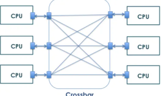
Figure 8: A crossbar connecting CPU nodes
A crossbar has every node of the network connected to every other node, as depicted in Figure 8. This network topology is non-blocking because any node can send simultaneous messages to every other
node in the system without conflicts. Arbitration only happens on a per-target basis, significantly reducing arbitration bottlenecks. Furthermore, the direct connections allow for O(1) latency - each switch in the network directly connects the source node of a message to its destination node, so the message only has to traverse one "hop" in the network in order to be delivered. Crossbars also generally provide high bandwidth.
The downside of crossbars is that they can end up being tremendously expensive due to the use of too many wires. They are also not scalable. As the number of initiators and targets increased, muxes for wide buses became impractically large. To support continued system scaling, crossbars were cascaded with bridges between fabrics. Bridges between crossbars carried a significant cost in silicon area. They have also limited clock frequencies and significant transaction latencies.
As systems-on-chip grew in numbers of IP blocks, buses and crossbars revealed their limitations: shared buses resulted in contention, hierarchical bus and crossbar designs increased complexity. In the third generation, during the 2000s, the initiators and targets became so numerous and widely distributed in the physical floorplan of a chip that the crossbar became to complex in terms of physical wiring.
Packet-based, serialized Network-on-Chip (NoC) technology emerged as a solution to the wiring prob-lem. A packet is a standard form for representing information in a form adequate for communication. One packet may correspond to a fraction, one or even several messages. In the context of NoCs, pack-ets are frequently a fraction of a message. Packpack-ets are often composed by a header, a payload and a trailer. Furthermore, distributing the interconnect logic throughout the chip rather than having bridges as chokepoints greatly simplified floor planning of the most complex chips. NoC technology allowed a trade-off between throughput and physical wires at every point within the on-chip communication network.
3.2
Basic concepts on Network-on-Chip
Network-on-Chips have been introduced for addressing the communication scalability challenge faced with traditional mechanisms such as buses. This issue resulted from the growing number of cores/processors in modern systems-on-chip (SoC). NoCs provide such complex SoCs with better performance and power consumption by allowing parallel communications. Figure 9a shows an example of a NoC-based manycore architectures with distributed memory.
It is made of tiles communicating with each other by exchanging packets through the NoC. Each tile contains at minimum a router, a core, and a private memory. The router is dedicated to receive and forward packets over the NoC. Among existing NoC topologies, the 2D-mesh illustrated in Figure 9a is one of the most used. As for distributed systems, routing, flow control and resource arbitration are required in NoCs. Routing consists in deciding which links of the NoC must be used to carry a message between different tiles. Flow control, also known as packet switching, decides the packet allocation to the internal router resources and to the NoC links. In case of conflict between packets, resource arbitration chooses which packet should be given priority.
(a) The NoC architecture is made of tiles, each com-prising a core, a private memory and a router allow-ing communication with other tiles
(b) Router with virtual channels. Each input port has several virtual channels used to store flits. The packet switching block allocates output resources to input flits
Figure 9: Example of a 2D-mesh NoC-based manycore architecture with distributed memory [87]
3.2.1 Topology
Topology refers to the static arrangement of channels and nodes in an interconnection network. A topology is chosen based on its cost and performance. The cost is determined by the number and complexity of the chips required to realize the network, and the density and length of the interconnections, on boards or over cables, between these chips. We consider the performance by measuring bandwidth and latency. Even if both of these measures are determined by factors other than topology like flow control, routing strategy, and traffic pattern, the topology is always the first thing to decide when building a NoC.
In the literature, the predominant network topology is the 2D Mesh topology (Figure 9a). The reason behind this choice derives from its three main advantages: facilitated implementation using current IC planar technologies, simplicity of the XY routing strategy and network scalability. Another approach is to use the 2D torus topology (Figure 10a), to reduce the network diameter, which is the maximum shortest path length between any pair of routers in the topology. The main issue of mesh and torus topologies is the associated network latency. Two alternatives have been proposed to face this problem: fat-tree topology (developed in Section 3.3.1) and chordal ring topology (Figure 10b), an extension of the existing ring topology (Figure 10c). Both approaches lead to a smaller network diameter, with a consequent latency reduction [71]. Finally, another topology has been proposed: the butterfly, depicted on Figure 10d. Compared to the others, it ensures that for N IP cores connected through the network, the butterfly is the topology with the minimal diameter that is necessary for connecting these N IPs [23]. One of the main drawback is that this topology cannot be implemented without long wires that must cross at least half the diameter of the network. Because the speed of a wire decreases quadratically with distance over the critical length [23], these long wires make butterflies less attractive for moderate and large-sized interconnection networks. However, the logarithmic
diameter and simple routing of the butterfly network has made it and its variants some of the most popular of interconnection networks for many applications.
(a) A Torus network (b) A cordal-ring network
(c) A ring network
(d) A butterfly network
Figure 10: Different Network-on-Chip topologies [23]
3.2.2 Communication through packets
As shown on Figure 11, the flits are the basic elements composing a packet. Many routing algorithms and flow control mechanisms have been proposed in the literature [23]. Figure 9b depicts the router architecture supporting the packet switching and arbitration policies. Each router of a NoC comprises a fixed number of ports depending on the topology (some ports may not exist for routers at the boundaries). Some ports are used to communicate with neighboring tiles. One extra port, called local port, allows communication with the core of the tile. Each port contains several buffers, called virtual channels, which temporarily store the flits of exchanged packets. These buffers provide a better utilization of the NoC links by storing blocked flits and still making usable the resources of the router and the links of the NoC. The arbitration block handles resource allocation in case of conflicts between
packets. Different arbitration policies exists such as oldest-first or priority-based [23]. The priority of a flit is assigned according to the priority of the packet containing the flit. This packet priority is set up by packet producers (cores) before sending them into the NoC.
Figure 11: An example of a packet in a Network-on-Chip
3.2.3 Flow Control
Flow control defines how shared resources i.e. channel bandwidth and buffer capacity are used when contention occurs. Buffers are used by routers to store packets between each hop. A channel consists of two one-directional point-to-point buses between two routers or a routers and a resource. A good flow control method allocates these resources in an efficient manner so the network achieves a high bandwidth and delivers packets with low and predictable latency.
Flow control can be viewed as either a problem of resource allocation or one of contention resolution. From the resource allocation perspective, resources in the form of channels and buffers must be allocated to each packet as it advances from the source to the destination. The same process can be viewed as one of resolving contention. For example, two packets arriving on different inputs of a router at the same time may both desire the same output. In this situation, the flow control mechanism resolves this contention, allocating the channel to one packet and somehow dealing with the other, blocked packet.
There exist three main protocols to achieve flow control (Table 2):
Store-and-Forward Store-and-forward routing is a packet switched protocol in which each router stores the complete packet and forwards it based on the information within its header. Thus, the packet may stall if the router in the forwarding path does not have sufficient buffer space.
Wormhole switching In the wormhole switching, when a packet header flit arrives to a router input channel, it is forwarded to an output channel as soon as the output channel is available. Then, the packet is scheduled (even if the packet payload flits are still flowing on the network). When the header is forwarded to the required output channel, the payload flits follow it in a pipeline fashion. However, if the required output is busy and the packet header flit is not scheduled, then the router must implement some buffer space to store some of the payload flits. The other flits must be stored in the previous routers in the packet path. The main advantage of the wormhole switching is to allows to build small and fast routers
Virtual cut-through Virtual cut-through routing has a forwarding mechanism similar to that of wormhole routing. But before forwarding the first flit of the packet, the router waits for a guarantee that the next router in the path will accept the entire packet. Thus if the packet stalls, it aggregates in the current router without blocking any links.
Protocol Per router cost Stall
Latency Buffering
store-and-forward packet packet at two routers and the link between them
wormhole header header at all routers and links spanned by the packet
virtual cut-through header packet at the local router
Table 2: Cost and Stalling for Different Routing Protocols [16]
3.2.4 Routing strategy
The routing strategy defines which path a packet takes from its sources to its destination. Routing algorithms can be generally classified as deterministic routing and adaptive routing.
Deterministic routing strategy benefits from its simplicity in router design. Another advantage of that is its speed. Because routers do not need to communicate with their peers to compute the next hop, the routing algorithm is very fast, which leads to a fast forwarding of packets. However, it is likely to suffer from throughput degradation when the packet injection rate increases. Indeed, the network contention cannot be avoided due to static decisions.
An example of such strategy is the "X-first" [22] strategy, described by the figure 12. When a packet comes from (0,3) and its destination is (2,2), the routing strategy is to go as far as possible in the X direction (east or west), and then in the Y direction (north or south).
Figure 12: Example of dimension-order routing in a 6x6 2D-torus. A packet is routed from node s= 03 to node d = 22 first routing in the x dimension and then in the y dimension [23]
Dynamic strategies [5, 68] are the complete opposite. The route for a packet is never known in advance and is compute at every hop based on the congestion conditions in the network. This kind of strategy has major advantages compared to the static routing. The NoC is aware of the amount of packets that
are on the network and it can adapt its routing strategy to avoid contention on a subset of routers and link by choosing a new path for a class of packets. The adaptiveness reduces the chance for packets to enter hotspots or faulty components, and hence reduces the blocking probability of packets.
To ensure proper operation during message transfers, a NoC must avoid deadlock, livelock and starvation. Deadlock may be defined as a cyclic dependency among nodes requiring access to a set of resources so that no forward progress can be made regardless the sequence of events that occurs. Livelock refers to packets circulating the network without ever making any progress towards their destination. It may be avoided with adaptive routing strategies. Starvation happens when a packet in a buffer requests an output channel being blocked because it is always allocated to another packet. As a global summary, Table 3 reports the main advantages and limitations of NoCs and buses [103].
Criteria NoC Bus
Bandwidth & speed Concurrent transactions -Pipelined links (higher through-put)
A transaction blocks other transac-tions in a shared bus
Resource utilization Shared links between transactions A single master occupies a shared bus during its transaction
Reliability Earlier detection of link/packet-level error control, shorter switch-2-switch links, reroute made possible in case of fault
Longer bus-wire are error-prone, a fault path is a system failure
Arbitration Smaller (thus faster) distributed ar-biters
Central arbiter (potentially big and slow)
Transaction energy Point-2-point connection consumes minimum transaction energy
Broadcast transaction need more en-ergy
Modularity & Complexity Switch/Link designs is re-instantiated. Communication and complexity decoupled
Bus design often specific
Scalability Global bandwidth scales with
net-work size
A shared bus becomes slower as the design gets bigger and thus is less scalable
Clocking GALS-like design Master clock for synchronizing
Latency Repeated arbitration/switch,
packetiz-ing, synchronizing and interfacing
Wire speed (once a master has grant from arbiter)
Overhead More routers/switches leads to more
area & power
Less area & buffer
Table 3: Summary of buses and NoCs properties [103]
3.3
Examples of 2D Network-on-Chip
3.3.1 Academic versions
SPIN The Scalable Programmable Interconnection Network (SPIN) [8, 36] is a packet switching Network-on-Chip that uses wormhole switching, adaptive routing and credit-based flow control. It considers a fat-tree topology, i.e., a tree structure with routers on intermediate nodes and terminals
Figure 13: Example of the SPIN Network-on-Chip with 32 IP blocks, 4 per router
on the leaves. Authors chose a full 4-ary fat-tree topology, illustrated in Figure 13 to produce a non-blocking network with a performance that scales gracefully with the system size.
HERMES HERMES [71] considers a 2D-mesh NoC that implements packet-switching as flow control. A router is composed of routing control logic and five bi-directional ports corresponding to four neighbor routers (East, West, North, South) and to a local port as already illustrated in Figure 9b The router employs an XY routing algorithm. A main design objective of Hermes was to develop a small size router.
3.3.2 Industrial versions
MPPA The Multi-Purpose Processor Array (MPPA) [24] of Kalray is a manycore architecture that integrates 256 user cores and 32 system cores in 28nm CMOS technology, where the cores are distributed across 16 compute clusters of 16+1 cores, and 4 quad-core I/O subsystems. Each compute cluster has a private local memory and cache coherence is enforced by software. Communication and synchronization between compute clusters are ensured by a proprietary NoC using a 2D torus topology with a wormhole routing.
Each MPPA-256 compute cluster (Figure 14a) comprises a banked parallel memory shared by cores. The other bus masters on the shared memory are the NoC Rx interface for receiving packets, the NoC Tx interface for packets transmission, and the debug support unit (DSU).
As described in [24], the 16 compute clusters and the 4 I/O subsystems are connected by two parallel NoC with bi-directional links, one for data (D-NoC), and the other for control (C-NoC). There is one NoC node per compute cluster, and four nodes per I/O subsystem. Each NoC node is associated with a D-NoC router and a C-NoC router. The two NoC are identical with respect to the nodes, the 2D torus topology with off-chip extensions (Figure 14b), and the wormhole route encoding. They differ at their device interfaces, and by the amount of packet buffering in routers. NoC traffic through a router does not interfere with the memory buses of the underlying I/O subsystem or compute cluster, unless the NoC node is a destination.
Tile64 The Tile64 [11] processor is a multicore System-on-Chip that has been proposed to fill the high-performance demands from various application domains. Figure 15b shows a block diagram with 64 tile processors arranged in an 8×8 array.
(a) A single tile of the MPPA (b) Overview of the MPPA Network-on-Chip
Figure 14: The MPPA-256 cores System-on-Chip [24]
These tiles, depicted in figure 15a, are connected through five scalable 2D mesh networks with high-speed I/Os on the periphery. No hardware virtual channels are required on any network. Each network data width is independent of the other networks. The network routing logic is included in the SoC building blocks. Networks use the wormhole routing algorithm. The switch, is a full crossbar for non-blocking routing, with credit-based flow control.
(a) Single tile block diagram (b) Tile64 block diagram
Figure 15: Overview of the Tile64 System-on-Chip [11]
3.4
Towards 3D Network-on-Chip
More recently, three-dimensional (3D) stacked technologies opened new opportunities for on-chip interconnect design. 3D integrated circuits (ICs) combine multiple layers of running heterogeneous devices, while reducing the length of interconnects. They provide a significantly increased package
density, a reduced power thanks to shorter wires, and noise-insensitive circuitry. All these benefits contribute in enhancing the global system performance and power consumption.
Several 3D vertical interconnect technologies have been investigated, such as micro-bump, wire bonding, contactless interconnect (e.g. capacitive or inductive), and Through-Silicon-Via (TSV), which appears as the most promising technology . These technologies also come with new memory hierarchy organization possibilities, mainly divided into stacking cache-only architectures and stacking main memory architectures for 3D multiprocessor System-on-Chip.
The most frequently 3D topology is the mesh, depicted in Figure 16. It relies on an extension of 2D mesh topology, where in addition to existing links, each node has two additional links (up and down) for inter-layer communications.
Figure 16: A 3D Mesh with TSVs on several tiles [102]
The convergence of NoC and 3D IC makes it possible to devise 3D NoCs, which aggregate the advantages of both paradigms. More detailed discussion on recent research and practices 3D NoC architectures could be found in literature [59, 67].
3.5
Performance metrics
To compare and contrast different NoC architectures, a standard set of performance metrics can be used. For example, it is desirable that a Network-on-Chip exhibits high throughput, low latency, energy efficiency, and low area overhead. In today’s power constrained environments, it is increasingly critical to be able to identify the most energy efficient architectures and quantify the energy-performance trade-offs.
Throughput Typically, the performance of a communication network is characterized by its band-width in bits/sec, or the rate at which message traffic can be sent across the network, also called throughput. Throughput can be defined in a variety of different ways depending on the specific na-ture of the implementation. For message passing systems, we can define message throughput, T P , as follows [80]:
where Total messages completed refers to the number of whole messages that successfully arrive at their destination IPs, Message length is measured in flits, Number of IP blocks is the number of functional IP blocks involved in the communication, and Total time is the time (in clock cycles) that elapses between the occurrence of the first message generation and the last message reception. Thus, message throughput is measured as the fraction of the maximum load that the network is capable of physically handling. An overall throughput of T P = 1 corresponds to all end nodes receiving one flit every cycle. Accordingly, throughput is measured in flits/cycle/IP. Throughput means the maximum value of the accepted traffic and it is related to the peak data rate sustainable by the system.
Latency Transport latency is defined as the time (in clock cycles) that elapses between the occurrence of a message header injection into the network at the source node and the occurrence of a tail flit reception at the destination node. To reach the destination node from some starting source node, flits must travel through a path consisting of a set of switches and interconnect. Depending on the source/destination pair and the routing algorithm, each message may have a different latency. There is also some overhead in the source and destination that also contributes to the overall latency. Therefore, for a given message i, the latency Liis [80]:
Li = sender overhead + transport latency + receiver overhead
For overall performance evaluation, the average latency can be used. P is the total number of messages reaching their destination IPs and Li represents the latency of each message i, where i ranges from 1
to P . The average latency, Lavg, is then calculated according to the following [80]:
Lavg = P X i=1 Li P
Saturation point A common metric used to measure network performance is the saturation through-put, defined as the network throughput at which the first channel saturates [23]. Each of the network’s properties establishes a bound on its performance: the network channel bandwidth, the topology im-poses an initial throughput, and the latency bound governed by the network diameter. The routing algorithm also offers different trade-offs for achievable performance; e.g. non-minimal routing can in-crease the latency while increasing the throughput. Finally, flow control and router micro-architecture introduce router efficiency and contention effects that can further limit the network performance. As presented in Section 3.4, 3D-NoCs are often based on TSVs. However, TSVs could suffer from various manufacturing defects [96, 48] such as misalignment, impurities, voids, pinholes and cracks. In [29], authors tackle this problem by evaluating the overall network performances with variable TSV quality. They modeled different TSVs quality and position on the mesh, injected packets thought the network and then evaluated the saturation point (Figure 17). As expected, the better the TSVs are, the later the saturation point occurs.
Figure 17: Average packet latency vs. injection rates. P1 represents the best TSV quality, P2 the medium quality and P3 the worst TSV quality [29]
Link load Another important metric is the link load. This value could be use to determine the specific parts of the network that are potentially subject to congestion.
Let Nx the overall number of packets transferred on a link x. Each link defines this value. Let Nmax
the maximum value of all Nx. The link x with this Nmaxhas a link load value Lx = 1. Hence, the
link load value for all links is computed as follows:
Lx = NNmaxx
In [50], authors used different mappings for a given application executed on a 2D-Mesh multicore architecture in order to find the best execution performances for the application. Based on the McSim [49, 50] simulator, they obtained the link load for all links as depicted by Figure 18. Figure 18a shown on the left presents such result with a zigzag mapping on the NoC. Conversely, Figure 18b shown on the right gives the same analysis with another mapping named local-maximized. In the latter case, tasks are mapped close to the locations where their main accessed data are mapped, so as to reduce high communication cost.
Energy consumption The energy consumption of a system could be divided into two parts: static and dynamic energy consumption. The dynamic energy is the amount of energy that is needed to ensure the propagation of the information. Indeed, when flits travel on the interconnection network, both wires and logic gates in the routers toggle and it results in energy dissipation. Conversly, the static energy is the amount of energy that each component must used to stay on. Here, we are focusing on the dynamic energy dissipation caused by the communication process in the network. The flits from the source nodes need to traverse multiple hops consisting of routers and wires to reach destinations. Consequently, we determine the energy dissipated by the flits in each wire and router hop. The energy per flit per hop is given by:
(a) Average load on all channel with a Zigzag map-ping
(b) Average load on all channel with a local-maximized mapping
Figure 18: McSim results
where Erouter and Ewiredepend on the total capacitance and signal activity of the router and each
section of interconnect wire, respectively. The energy dissipated in transporting a packet consisting of n flits over h hops can be calculated as:
Epacket = n h
X
j=1
Ehop.j
The BookSim simulator (presented in 3.6) produces different metrics in its simulation output, related to power and area:
• total power consumption, • wires and routers leakage, • wire and routers dynamic power, • wires and routers area,
• etc.
More details could be found in the Booksim paper [75] and user guide [74].
3.6
Simulation tools
BookSim is a cycle-accurate NoC simulator developed at Stanford university. It has been originally designed and introduced to support the book Principles and Practices of Interconnection Networks [23].
Then, it has been extended with many recent features of NoC design. The current major release, BookSim 2.0 [75], supports a wide range of topologies such as mesh, torus and flattened butterfly networks, provides diverse routing algorithms and includes numerous options for customizing the network’s router micro-architecture. BookSim is written in C++ but does not rely on the SystemC simulation library.
Garnet [4] models a NoC at the cycle-accurate level. The model allows either a standard virtual channel router with a five-stage pipeline, or a flexible router with configurable pipeline. Its integration with the gem5 simulator [14] provides a full-system simulation framework and a memory model, while its integration with ORION [45] provides power estimation.
TOPAZ [3] is another cycle-accurate network on chip simulator. TOPAZ can be used standalone through synthetic traffic patterns and application-traces or within full-system evaluation systems such as gem5. TOPAZ enables the modeling of a wide variety of message routers, with different trade-offs between speed and precision.
NoCTweak [97] is a cycle-accurate NoC simulator for 2D-mesh topologies. It is written in C++/SystemC and is designed around two main abstractions. The first one represents a core of the simulated hardware while the second one represents a router. NoCTweak provides two different types of cores. The first one, called Synthetic, describes cores that only inject packets into the network either in a uniform random fashion or with particular hotspots. The second type of cores, called Em-bedded, can be used to inject packets according to traces from real embedded applications. Regarding the routers, NoCTweak also provides two different types. The first one is the widespread wormhole router architecture where packets are divided into flits. The first flit is called the header-flit, and all other flits follow the route opened by the header one. The second type of router provided has virtual channels. Like in wormhole, the packets to be exchanged are divided into flits, but in this case each router has several virtual channels to make a better use of the routers resources by allowing several packets to be stored and processed in a given router at the same time.
ModelSim [66], a software developed by the Mentor Graphics company, is well suited software to simulate digital components based on the hardware description languages VHDL (Very High Speed Integrated Circuits Hardware Description Language) and Verilog. One of the advantage of ModelSim is its low-level granularity. As an example, the latency of each component is accounted at the gate-level granularity. This approach makes it possible to accurately analyze various metrics such as bandwidth and communication latencies in the NoC [29]. Another advantage is the possibility to model 3D Network-on-Chips with a high level of accuracy compared to non-commercial solutions. Finally, we can mention high-level modeling and simulation approaches relying on SystemC [38, 65, 49, 50] and UML [30, 33, 86, 9] for instance. The MARTE standard has been used to model complex NoC topologies in [30]. The resulting descriptions can be afterwards transformed according to model-driven engineering to derive simulable (or executable) NoC models.
3.7
Summary
In this chapter, we presented an overview of the on-chip interconnect paradigm. The described interconnect models are made of components that can operate independently without global control requirements and meet the increasing need for more computation performance on a single chip.
We discussed some relevant features in the design of such interconnects including topology, flow control, routing, and we presented several metrics to evaluate the choice of these feature. Moreover, we presented academic and industrial NoCs and briefly described 3D Network-on-Chip which is a promising technology in terms of performance and power consumption.
4
Conclusions
This deliverable presented a survey of existing emerging memory and communication technologies. It first provided an overview on non-volatile memories with a focus on magnetic memories, which are identified as a very promising solution to energy reduction. Then, a general presentation of on-chip communication interconnects, and mainly networks-on-on-chip (NoCs), was given. The discussed technologies are relevant ingredients that are expected to be explored within the design of the compute node architectures targeted by the CONTINUUM project.
From the current survey, we plan to devise architecture models that integrate MRAM technology in memory hierarchy, and to evaluate the overall outcome on energy/performance trade-off. Various software-level execution decisions will be considered on such architectures models, e.g., different compilation techniques, in close collaboration with the Inria partner of the project. The target architectures will be composed of various types of embedded cores, e.g., Cortus or ARM, while the interconnects will cover both buses and on-chip networks. The final aim of this multicore / manycore architecture exploration in presence of NVMs and on-chip interconnects combined with compilation techniques is to draw the compute node model studied in CONTINUUM.
References
[1] Crocus technology company. URL http://www.crocus-technology.com/. [2] Everspin company. URL http://www.everspin.com/.
[3] Abad, P., Prieto, P., Menezo, L. G., Colaso, A., Puente, V., and Gregorio, J. Topaz: An open-source interconnection network simulator for chip multiprocessors and supercomputers. In 2012 IEEE/ACM Sixth International Symposium on Networks-on-Chip, pages 99–106, 2012. doi: 10.1109/NOCS.2012.19.
[4] Agarwal, N., Krishna, T., Peh, L., and Jha, N. K. Garnet: A detailed on-chip network model inside a full-system simulator. In 2009 IEEE International Symposium on Performance Analysis of Systems and Software, pages 33–42, 2009. doi: 10.1109/ISPASS.2009.4919636.
[5] Ali, M., Welzl, M., and Hellebrand, S. A dynamic routing mechanism for network on chip. In 2005 NORCHIP, pages 70–73, 2005. doi: 10.1109/NORCHP.2005.1596991.
[6] Amiri, P. K., Upadhyaya, P., Alzate, J., and Wang, K. Electric-field-induced thermally assisted switching of monodomain magnetic bits. Journal of Applied Physics, 113(1):013912, 2013. [7] Andre, T. W., Nahas, J. J., Subramanian, C. K., Garni, B. J., Lin, H. S., Omair, A., and
Martino Jr, W. L. A 4-mb 0.18-µm 1t1mtj toggle mram with balanced three input sensing scheme and locally mirrored unidirectional write drivers. Solid-State Circuits, IEEE Journal of, 40(1):301–309, 2005.
[8] Andriahantenaina, A., Charlery, H., Greiner, A., Mortiez, L., and Zeferino, C. A. SPIN: A scalable, packet switched, on-chip micro-network. In 2003 Design, Automation and Test in Europe Conference and Exposition (DATE 2003), 3-7 March 2003, Munich, Germany, pages 20070–20073. IEEE Computer Society, 2003. doi: 10.1109/DATE.2003.10240. URL http://doi.ieeecomputersociety.org/10.1109/DATE.2003.10240. [9] Apvrille, L. and Bécoulet, A. Prototyping an Embedded Automotive System from
its UML/SysML Models. In Embedded Real Time Software and Systems (ERTS2012), Toulouse, France, February 2012. URL https://hal.archives-ouvertes.fr/hal-02191862.
[10] Baibich, M. N., Broto, J. M., Fert, A., Van Dau, F. N., Petroff, F., Etienne, P., Creuzet, G., Friederich, A., and Chazelas, J. Giant magnetoresistance of (001) fe/(001) cr magnetic superlattices. Physical review letters, 61(21):2472, 1988.
[11] Bell, S., Edwards, B., Amann, J., Conlin, R., Joyce, K., Leung, V., MacKay, J., Reif, M., Bao, L., Brown, J., Mattina, M., Miao, C., Ramey, C., Wentzlaff, D., Anderson, W., Berger, E., Fairbanks, N., Khan, D., Montenegro, F., Stickney, J., and Zook, J. Tile64 - processor: A 64core soc with mesh interconnect. In 2008 IEEE International SolidState Circuits Conference -Digest of Technical Papers, pages 88–598, 2008. doi: 10.1109/ISSCC.2008.4523070.
[12] Benini, L. and De Micheli, G. Networks on chips: a new soc paradigm. Computer, 35(1): 70–78, 2002. doi: 10.1109/2.976921.
[13] Binkert, N., Beckmann, B., Black, G., Reinhardt, S. K., Saidi, A., Basu, A., Hestness, J., Hower, D. R., Krishna, T., Sardashti, S., Sen, R., Sewell, K., Shoaib, M., Vaish, N., Hill, M. D., and Wood, D. A. The gem5 simulator. SIGARCH Comput. Archit. News, 39(2):1–7, August 2011. ISSN 0163-5964. doi: 10.1145/2024716.2024718. URL https://doi.org/10.1145/ 2024716.2024718.
[14] Binkert, N., Beckmann, B., Black, G., Reinhardt, S. K., Saidi, A., Basu, A., Hestness, J., Hower, D. R., Krishna, T., Sardashti, S., et al. The gem5 simulator. ACM SIGARCH Computer Architecture News, 39(2):1–7, 2011.
[15] Bishnoi, R., Ebrahimi, M., Oboril, F., and Tahoori, M. B. Architectural aspects in design and analysis of sot-based memories. In Design Automation Conference (ASP-DAC), 2014 19th Asia and South Pacific, pages 700–707. IEEE, 2014.
[16] Bjerregaard, T. and Mahadevan, S. A survey of research and practices of network-on-chip. ACM Comput. Surv., 38(1):1–es, June 2006. ISSN 0360-0300. doi: 10.1145/1132952.1132953. URL https://doi.org/10.1145/1132952.1132953.
[17] Butko, A., Gamatié, A., Sassatelli, G., Torres, L., and Robert, M. Design exploration for next generation high-performance manycore on-chip systems: Application to big.little architectures. In 2015 IEEE Computer Society Annual Symposium on VLSI, ISVLSI 2015, Montpellier, France, July 8-10, 2015, pages 551–556. IEEE Computer Society, 2015. doi: 10.1109/ISVLSI.2015.28. URL https://doi.org/10.1109/ISVLSI.2015.28.
[18] Butko, A., Bruguier, F., Gamatié, A., Sassatelli, G., Novo, D., Torres, L., and Robert, M. Full-system simulation of big.little multicore architecture for performance and energy exploration. In 10th IEEE International Symposium on Embedded Multicore/Many-core Systems-on-Chip, MCSOC 2016, Lyon, France, September 21-23, 2016, pages 201–208. IEEE Computer Soci-ety, 2016. doi: 10.1109/MCSoC.2016.20. URL https://doi.org/10.1109/MCSoC. 2016.20.
[19] Butler, W., Zhang, X.-G., Schulthess, T., and MacLaren, J. Spin-dependent tunneling conduc-tance of fe| mgo| fe sandwiches. Physical Review B, 63(5):054416, 2001.
[20] Chen, K., Li, S., Muralimanohar, N., Ahn, J. H., Brockman, J. B., and Jouppi, N. P. Cacti-3dd: Architecture-level modeling for 3d die-stacked dram main memory. In Proceedings of the Conference on Design, Automation and Test in Europe, pages 33–38. EDA Consortium, 2012. [21] Chen, Y.-T., Cong, J., Huang, H., Liu, C., Prabhakar, R., and Reinman, G. Static and dynamic co-optimizations for blocks mapping in hybrid caches. In Proceedings of the 2012 ACM/IEEE international symposium on Low power electronics and design, pages 237–242. ACM, 2012.
[22] Dally and Seitz. Deadlock-free message routing in multiprocessor interconnection networks. IEEE Transactions on Computers, C-36(5):547–553, 1987. doi: 10.1109/TC.1987.1676939.
[23] Dally, W. J. and Towles, B. P. Principles and practices of interconnection networks. Elsevier, 2004.
![Figure 3: SoC energy repartition between logic and memory (from ITRS [42])](https://thumb-eu.123doks.com/thumbv2/123doknet/14235230.486078/9.892.200.689.586.874/figure-soc-energy-repartition-logic-memory-itrs.webp)
![Figure 4: Magnetoresistance ratio evolution [104]](https://thumb-eu.123doks.com/thumbv2/123doknet/14235230.486078/13.892.198.678.144.495/figure-magnetoresistance-ratio-evolution.webp)
![Figure 5: Conventional MRAM [7]](https://thumb-eu.123doks.com/thumbv2/123doknet/14235230.486078/14.892.341.554.141.311/figure-conventional-mram.webp)

![Figure 9: Example of a 2D-mesh NoC-based manycore architecture with distributed memory [87]](https://thumb-eu.123doks.com/thumbv2/123doknet/14235230.486078/22.892.153.741.139.398/figure-example-mesh-based-manycore-architecture-distributed-memory.webp)
![Figure 10: Different Network-on-Chip topologies [23]](https://thumb-eu.123doks.com/thumbv2/123doknet/14235230.486078/23.892.139.726.169.803/figure-different-network-on-chip-topologies.webp)

![Figure 12: Example of dimension-order routing in a 6x6 2D-torus. A packet is routed from node s = 03 to node d = 22 first routing in the x dimension and then in the y dimension [23]](https://thumb-eu.123doks.com/thumbv2/123doknet/14235230.486078/25.892.328.561.736.971/figure-example-dimension-routing-packet-routing-dimension-dimension.webp)
![Table 3: Summary of buses and NoCs properties [103]](https://thumb-eu.123doks.com/thumbv2/123doknet/14235230.486078/26.892.88.808.396.858/table-summary-buses-nocs-properties.webp)
