Publisher’s version / Version de l'éditeur:
ACS Nano, 11, 4, pp. 3542-3552, 2017-02-27
READ THESE TERMS AND CONDITIONS CAREFULLY BEFORE USING THIS WEBSITE.
https://nrc-publications.canada.ca/eng/copyright
Vous avez des questions? Nous pouvons vous aider. Pour communiquer directement avec un auteur, consultez la
première page de la revue dans laquelle son article a été publié afin de trouver ses coordonnées. Si vous n’arrivez pas à les repérer, communiquez avec nous à [email protected].
Questions? Contact the NRC Publications Archive team at
[email protected]. If you wish to email the authors directly, please see the first page of the publication for their contact information.
NRC Publications Archive
Archives des publications du CNRC
This publication could be one of several versions: author’s original, accepted manuscript or the publisher’s version. / La version de cette publication peut être l’une des suivantes : la version prépublication de l’auteur, la version acceptée du manuscrit ou la version de l’éditeur.
For the publisher’s version, please access the DOI link below./ Pour consulter la version de l’éditeur, utilisez le lien DOI ci-dessous.
https://doi.org/10.1021/acsnano.7b00597
Access and use of this website and the material on it are subject to the Terms and Conditions set forth at
Structure controlled long-range sequential tunneling in carbon-based
molecular junctions
Morteza Najarian, Amin; Mccreery, Richard L.
https://publications-cnrc.canada.ca/fra/droits
L’accès à ce site Web et l’utilisation de son contenu sont assujettis aux conditions présentées dans le site LISEZ CES CONDITIONS ATTENTIVEMENT AVANT D’UTILISER CE SITE WEB.
NRC Publications Record / Notice d'Archives des publications de CNRC:
https://nrc-publications.canada.ca/eng/view/object/?id=6054a9b8-aeef-4ccb-8b58-2290cd56e38d https://publications-cnrc.canada.ca/fra/voir/objet/?id=6054a9b8-aeef-4ccb-8b58-2290cd56e38d
Structure Controlled Long-Range Sequential
Tunneling in Carbon-Based Molecular
Junctions
Amin Morteza Najarian
†,‡and Richard L. McCreery
*
,†,‡†
Department of Chemistry, University of Alberta, Edmonton,Alberta T6G 2R3, Canada ‡
National Institute for Nanotechnology, National Research Council Canada, Ottawa, Ontario T6G 2G2, Canada
*
S Supporting InformationABSTRACT: Carbon-based molecular junctions consisting of aromatic oligomers between conducting sp2 hybridized carbon electrodes exhibit structure-dependent current densities (J) when the molecular layer thickness (d) exceeds ∼5 nm. All four of the molecular structures examined exhibit an unusual, nonlinear ln J vs bias voltage (V) dependence which is not expected for conventional coherent tunneling or activated hopping mechanisms. All molecules exhibit a weak temperature dependence, with J
increasing typically by a factor of 2 over the range of 200−440 K. Fluorene and anthraquinone show linear plots of ln J vs d with nearly identical J values for the range d = 3−10 nm, despite significant differences in their free-molecule orbital energy levels. The observed current densities for anthraquinone, fluorene, nitroazobenzene, and bis-thienyl benzene for d = 7−10 nm show no correlation with occupied (HOMO) or unoccupied (LUMO) molecular orbital energies, contrary to expectations for transport mechanisms based on the offset between orbital energies and the electrode Fermi level. UV−vis absorption spectroscopy of molecular layers bonded to carbon electrodes revealed internal energy levels of the chemisorbed films and also indicated limited delocalization in the film interior. The observed current densities correlate well with the observed UV−vis absorption maxima for the molecular layers, implying a transport mechanism determined by the HOMO−LUMO energy gap. We conclude that transport in carbon-based aromatic molecular junctions is consistent with multistep tunneling through a barrier defined by the HOMO−LUMO gap, and not by charge transport at the electrode interfaces. In effect, interfacial “injection” at the molecule/electrode interfaces is not rate limiting due to relatively strong electronic coupling, and transport is controlled by the “bulk” properties of the molecular layer interior. KEYWORDS: molecular electronics, charge transport, multistep tunneling, thermally assisted tunneling, electronic coupling,
localization length
T
he field of molecular electronics (ME) investigates charge transport in single molecules or ensembles of molecules oriented between conducting contacts acting as elements in electronic circuits. A core principle in ME is the control of charge transport by variations in molecular structure and the possibly wide variety of electronic functions which may be available with molecular components but difficult with conventional semiconductors. Numerous experimental para-digms have been employed in extensive research on how structure controls transport, in alkane, aromatic, and oligomeric molecular junctions (MJs).1−5 A key parameter in charge transport is the length of the molecular component (d, in nm) between conducting contacts, and the dependence of MJ current on d is often a useful diagnostic for transport mechanism. For example, the exponential dependence of current density, J (A/cm2), at a given bias voltage on d is often cited as an indication of quantum mechanical tunneling,with the slope of ln J vs d yielding β, the attenuation coefficient with units of Å−1or nm−1.6 From transport measurements in donor−acceptor complexes, modified electrodes, and MJs of both single molecules and ensembles, β is generally accepted to equal 6−9 nm−1for aliphatic molecules,7−11while β is in the range of 2−5 nm−1for conjugated or aromatic molecules12−15 and <1 nm−1for certain metal complexes with strong electronic coupling between molecular subunits.16−18Carbon-based MJs with carbon/molecule/Cu or carbon/molecule/carbon struc-tures containing aromatic molecular layers exhibit β values of ∼2.1−3.3 nm−1 and a weak dependence on variations in structure for d < 5 nm due to strong electronic coupling between the molecules and contacts.13,15,19
Received: January 26, 2017
Accepted: February 26, 2017
Published: February 27, 2017
Article
Plots of ln J vs d for conjugated and aromatic MJs are often reported to extend from d < 1 nm to d = 5 nm, depending on molecular structure and experimental paradigm. For example, oligomers of phenyleneimines exhibit β = 3.0 nm−1for d < 4 nm, then a change in slope to β = 0.9 nm−1for d = 4 to 7.5 nm.20,21 A similar change in slope was reported for oligophenylethynyl molecules, with β = 0.9 nm−1for d = 1 to 2.5 nm and β = 0.3 nm−1for d = 2.5 to 5.1 nm.22In several cases, the change in slope was attributed to a change in mechanism from direct or coherent tunneling to “hopping” involving a series of steps between sites in the molecular layer.23,24For bis-thienyl benzene (BTB) oligomers in carbon-based MJs, linearity of the attenuation plot with β = 2.9 nm−1 was observed for d = 2−8 nm, then β = 1.0 nm−1for d = 8−16 nm and β ≈ 0.02 nm−1for 16−22 nm. For BTB, the 1.0 nm−1 region extended from d = 8 to 22 nm at low temperature, thus ruling out activated redox exchange.25The general consensus to date associates the linear β ∼ 3 nm−1 region for conjugated molecules to direct tunneling, with a barrier determined by the offset between the electrode Fermi level and the molecular orbital closest in energy. Such transport may involve “electron tunneling” mediated by the molecular LUMO or “hole tunneling” mediated by the HOMO and is often referred to as the “single level model”.26,27For transport distances above
3−5 nm in conjugated molecules, several alternatives to coherent tunneling have been proposed, including redox exchange,21,28 polaron tunneling,29 and field ionization,25 although coherent tunneling remains a possibility.17 The dependence of junction current on temperature, thickness, and bias is valuable for determining transport mechanism, and each mechanism may be affected by molecular structure quite differently.
Our laboratory has studied carbon-based MJs containing aromatic oligomers covalently bonded to conducting carbon surfaces, with Cu or carbon/Au top contacts. For molecular layer thicknesses in the range of 2−5 nm, transport has the characteristics of coherent tunneling, with weak temperature dependence and linear attenuation plots with β = 2.7 ± 0.6 nm−1 for seven different aromatic structures and >400 MJs.15
However, both β and current density were very similar for aromatic structures, despite a variation of >2.3 eV in the HOMO and LUMO levels of the free molecules. We attributed this result to strong electronic coupling between the molecules and the contacts, which reduces the influence of electron-donating or -withdrawing groups on the observed transport barrier. Strong coupling between graphitic electrodes and aromatic molecules is also predicted theoretically, leading to significant shifts in HOMO and LUMO levels in graphene-molecule model structures relative to those of the free molecules.30−32 The current investigation was undertaken to address two questions about transport through organic films with thicknesses >5 nm. First, how far does the exponential dependence on layer thickness extend past 5 nm; and second, what transport mechanisms become operative once coherent tunneling becomes negligible? Three aromatic molecular layers that could be extended to thicknesses >5 nm were examined and compared to past results for a thiophene derivative in the same thickness range. A detailed analysis of the current−voltage response of diazonium-derived fluorene oligomers between carbon contacts and d = 2.3 to 8.6 nm revealed an unexpected behavior which is inconsistent with either coherent tunneling or the “single level” model commonly applied to aromatic MJs. Comparison to anthraquinone (AQ) and nitroazobenzene (NAB) MJs permitted insights into the factors controlling charge transport, and a multistep tunneling mechanism explains the experimental results.
RESULTS
Fluorene (FL) molecular junctions with thicknesses (d) of 2.3− 8.6 nm were examined in detail initially in order to characterize transport for molecular layers with d > 5 nm.Figure 1a shows a junction schematic and cross section of a completed device as well as the structure of FL and its oligomer. After describing their JV behavior, temperature dependence, and UV−vis absorption, additional MJs containing NAB, AQ, and BTB were examined for comparison, before proposing a transport mechanism.Figure 1b shows the four aromatic molecules used in the current work, with the density functional theory (DFT)-Figure 1. (a) Schematic illustration of PPF/FL/eC10/Au20molecular junction; n is a number of repeating units of oligomer that determines final thickness of molecular layer. (b) Structures and frontier orbital energy diagram for FL, AQ, NAB, and BTB, relative to a vacuum reference. Orbital energies were calculated by DFT B3LYP 6-31G(d), in Gaussian 09. Fermi level of PPF and eC is −4.8 V vs vacuum.
predicted energy levels of the free molecules relative to the vacuum level.
Fluorene JV Behavior.Current density vs bias voltage (JV) curves for FL MJs with 13 thicknesses in the range of 2.3−8.6 nm are shown inFigure 2a. Error bars on the response for 6.1 nm thickness indicate typical standard deviations of J, and all curves are averages of four separate MJs. Additional statistics and sample JV curves are available inSupporting Information
(SI) section 2 and Figure S5. The same results are shown in semilog format inFigure 2b, with error bars shown for the 6.1 nm case. Comparison of the JV curves clearly illustrates that (i) junction conductance depends nonlinearly on bias; (ii) JV curves are nearly symmetric with respect to bias polarity for all thicknesses; and (iii) there is a strong thickness dependence of conductivity, with conductance decreasing monotonically with thickness at all bias values. Note also that the ln J vs V curves do not exhibit the linearity expected for direct tunneling, and this point will be discussed in more detail below. Attenuation plots of ln J vs junction thickness (d) are shown inFigure 2c, for three bias values. For V = 0.3 V, β = 2.72 nm−1, in good agreement with that reported previously for seven other diazonium-derived aromatic junctions (β = 2.7 ± 0.6 nm−1)15 and β = 2.9 nm−1 for BTB devices with d < 8 nm.25 Note particularly that the exponential decrease in current density for FL devices extends well beyond the usual limit for direct tunneling of 3−5 nm, with minor changes in slope over the entire 2.3−8.6 nm range. A further test of the similarity of the JV response for different thicknesses is an overlay of the JV curves after normalization of the currents for all curves at V = 0.3 V to J = 1 A/cm2, as shown in Figure 2d. The 13 curve
shapes are very similar over the entire voltage range, implying that the J vs V behavior for all thicknesses has similar shape and dependence on bias.
As noted above, the nonlinearity of the ln J vs V plots in
Figure 2b is not expected for direct tunneling, and other transport mechanisms can result in such curvature. Poole− Frenkel transport between Coulombic traps and Schottky emission at interfaces can both predict linearity of ln J with V1/2, due to changes in the respective barriers with increases in electric field.33We considered these mechanisms previously for BTB devices in the thickness range of 8−12 nm, but rejected them due to inconsistency with the temperature dependence of the JV curves.25Figure 3shows ln J vs V1/2plots for comparison to ln J vs V inFigure 2b, and statistics for linear fits of ln J to V, ln J to V1/2, ln J/V to V1/2and other possible functional forms are listed inSupporting Information section 3 and Table S2. For d = 2.3−6.1 nm, the ln J vs V1/2plots are very linear, with R2 above 0.997 in all cases, while R2 for the ln J vs V plots ranges from 0.973 to 0.985. Slight upward curvature of the ln J vs V1/2plots is observed for d = 7.1 to 8.6 nm, but still results in a better linear fit (R2> 0.994 for d = 8.6 nm) than either ln J vs V (R2 > 0.985) or ln J/V vs V1/2 (R2 = 0.981). The slopes, intercepts, and R2values for linear fits of ln J vs V1/2plots of all 13 FL thicknesses are provided inTable S3.
Fluorene Temperature Dependence. We reported previously that BTB molecular junctions with d > 16 nm exhibited Arrhenius temperature dependence with Eact > 100 meV above 200 K, but thinner molecular layers and T < 200 T had apparent Arrhenius slopes in the range of 0−50 meV.25We
also reported that aromatic MJs with d < 5 nm had a weak Figure 2. (a) Current density vs bias voltage (JV) curves for PPF/FLd/eC10/Au20; d is a thickness of FL molecular layer: d = 2.3, 3.0, 3.4, 3.8, 4.1, 4.5, 5.0, 5.5, 6.1, 7.1, 7.6, 8.0, 8.6 nm in the order indicated. Each curve is an average of four independent junctions, with a typtical deviation shown for d = 6.1 nm junction. (b) Semilogarithmic plot of JV curves shown in panel a. (c) Corresponding attenuation plot for V = 0.3, 1.0, and 2.0 V, with the slopes (β) indicated. (d) Overlay of normalized semilogarithmic JV curves shown in panel b. Current density of each thickness was normalized to J = 1 A/cm2at 0.3 V.
temperature-dependent JV response, consistent with coherent tunneling with the addition of Fermi function broadening for T > 200 K.13 Tunneling in single porphyrin oligomers over a
distance to 5−10 nm exhibited Arrhenius slopes of 80−220 meV, but were concluded to be inconsistent with a hopping model.17The JV curves for FL devices with d = 5.5 nm shown inFigure 4a exhibit a weak dependence on temperature with J at 440 K less than twice that of J at 200 K. Plots of ln J vs V1/2 remain linear from 200 to 440 K (Figure 4b). The Arrhenius plots ofFigure 4c for two bias values show no linear regions, with a significant change in slope over the observed T range. Although these results are inconsistent with Arrhenius behavior, apparent activation energies (Eact) are provided over limited temperature ranges inFigure 4c andTable S4. For d = 5.5 nm
at V = 0.1 V, the apparent Arrhenius slopes are 8 meV in the 200−220 K range, 51 meV for 300−320 K, and 133 meV for 420−440 K. We found that the plots of ln J vs T shown in
Figure 4d are more linear than the Arrhenius format, with R2> 0.97 compared to <0.89 forFigure 4c. This fact remains valid for other measured thicknesses, and corresponding plots are provided inFigures S11 and S12. The linearity of ln J vs T from 240 to 440 K still indicates a temperature-dependent mechanism in this range, but clearly not classical Arrhenius behavior.
The temperature dependence of BTB was reported for a range of thicknesses previously25and is qualitatively similar to that of FL, with low apparent activation energies and curved Arrhenius plots. If the same BTB data are replotted as ln J vs T, linearity is observed for 8.1 and 10.4 nm, shown inFigure S14. AQ exhibits linearity of ln J vs T for four thicknesses (Figure S14), and NAB shows apparent Arrhenius slopes of <50 meV for d = 3.5, 8.0, and 35 nm.34
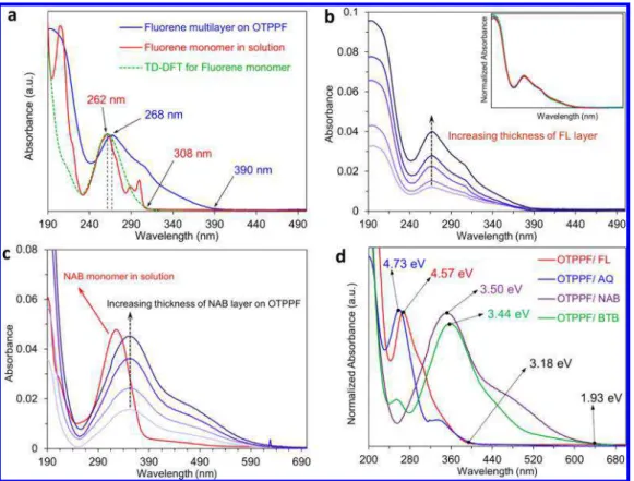
Optical Absorption by Molecular Layers. A direct indication of molecular orbital energies in the molecular layer is provided by the UV−vis absorption spectrum of FL bonded to optically transparent PPF (OTPPF) .35−37Here, we use UV− vis absorption to gain insight into electronic coupling within the molecular layer and between the molecules and the contacts.Figure 5a shows a UV−vis spectrum of FL monomer in acetonitrile, compared to that of a diazonium-derived FL molecular multilayer grafted on the surface of OTPPF. In the latter case, a spectrum of unmodified PPF was subtracted to reveal the molecular layer spectrum (as described inSupporting Informationsection 4).
There is a small (6 nm) red shift in the peak absorption wavelength upon FL bonding to PPF, but also an ∼80 nm red Figure 3. Natural log of current density vs square root of bias
voltage for the same series of FL junctions shown inFigure 2, for positive bias. Order of thickness is the same as inFigure 2a.
Figure 4. (a) JV curves for PPF/FL5.5/eC10/Au20junction at four temperatures from 200 to 440 K in vacuum. (b) ln J vs V1/2plots for curves in panel a. (c) Arrhenius plots at 0.1 and 0.3 V, with apparent activation energies for high and low T segments. (d) ln J vs T at 0.1, 0.3, and 0.5 V. R2for linear fits of the lines are indicated.
shift in the onset of the absorbance at 390 nm. At least some of this shift is due to electronic coupling30−32between the FL and the OTPPF and was reported previously for OTPPF/ nitroazobenzene bonded to OTPPF.36 Figure 5b shows the absorption spectra of four films of FL on OTPPF with thicknesses increasing from ∼2 to 9 nm, as indicated. The onset of absorbance at 390 nm does not change with increasing thickness, and the normalized spectra in the inset show that the entire spectrum shape is unchanged with thickness. Several authors have discussed a “localization length”38 or “effective conjugation length”39as the oligomer length where additional subunits no longer change the absorption spectrum.16,17,29,40 Tsuda et al.39reported that the localization length can extend to more than 12 fused coplanar porphyrin units with 175 nm red shift per subunit. However, the localization length in nonfused aromatic oligomers can be decreased by the nonzero dihedral angles of neighboring units and disordering in the molecular layer. For example, Choi et al. have shown that electronic coupling for conjugated oligophenyleneimine (OPI) wire extends over 3 repeating units with ∼100 nm red shift in the UV−vis absorption peak and then remains constant at 400 nm for longer OPI wires.21 In the present case of FL, however, increasing layer thickness does not change the absorption spectrum and is a direct indication of weak electronic coupling between FL subunits. The large red-shift of the absorbance onset which occurs for all thicknesses of FL multilayer grafted on the surface compared to FL monomer in solution may have at least three origins: (i) electronic coupling between FL and the graphitic π system of the carbon electrode; (ii) intermolecular π−π interactions in the FL layer; and (iii)
structural variations in FL−FL coupling within the molecular layer. At least over the thickness range examined, these effects do not produce an observable change in the UV−vis absorption spectrum with layer thickness. We conclude that a covalent bond between aromatic molecules is not enough to extend delocalization significantly beyond FL subunits in an oligomeric FL multilayer. The invariance of the UV−vis spectrum with thickness past a few nm clearly indicates weak electronic interactions between subunits and implies a localization length approximately equal to one or at most two FL molecules. Consideration of the molecular layer as a series of weakly interacting molecular orbitals is an important factor in controlling transport and is discussed in more detail below.
Structural Effects on Junction Behavior. To investigate effects of molecular structure on the electronic behavior observed for FL MJs, AQ and NAB films and devices were investigated and compared to BTB reported previously.25The UV−vis spectra of the FL, AQ, NAB, and BTB bonded to OTPPF are compared in Figure 5d after subtraction of the unmodified PPF spectrum, andTable 1lists the optical gap and absorption onsets as well as DFT predictions. Notice that both the peak absorption and onset of absorption occur at significantly lower energy for BTB and NAB compared to AQ and FL. As shown inFigure 5c, the absorption onset for NAB bonded to OTPPF also shows a significant red shift compared to NAB monomer in solution, but the peak and onset wavelengths do not vary further with increasing thickness. Additional absorbance spectra for the four molecules are provided in Supporting Informationsection 4, and the salient results are summarized inTable 1.
Figure 5. (a) Optical absorbance spectrum of FL monomer in acetonitrile (red) and FL multilayer bonded to the surface of OTPPF (blue), after subtraction of unmodified OTPPF spectrum. TD-DFT prediction of FL monomer spectrum is dashed green line. (b) Optical absorbance of four thicknesses of FL on OTPPF in the range of ∼2−9 nm. Inset: normalized spectra for different FL thicknesses. (c) Absorbance spectra of increasing thicknesses of NAB bonded to PPF, with that of NAB monomer in ACN for comparison (red). (d) Absorbance spectra for FL, AQ, NAB, and BTB multilayers bonded to OTPPF, all following subtraction of unmodified OTPPF spectrum.
Molecular junctions were fabricated with the same PPF/ molecule/eC/Au junction structure in all cases and d ranging from 3 to 13 nm. JV curves for the four molecules with similar thicknesses in the range of d = 7.4−8.1 nm are shown inFigure 6a, all exhibiting symmetry with bias and similar shape. However, J for BTB and NAB is much higher than that of FL and AQ, by a factor of ∼100 for V = ± 1 V. Complete sets for AQ and NAB are provided in Supporting Information
section 5 and Figures S9−S10. Plots of ln |J| vs V1/2 for the same examples are shown inFigure 6b, showing linearity similar to FL (R2 = 0.9902−0.9992 for all four cases) and large difference in J over the entire bias range. Complete sets of ln J vs V1/2curves for a range of thicknesses are provided inFigure S10for AQ, NAB and BTB.
A statistically more valid comparison of the four molecules over a wide thickness range is the attenuation plot ofFigure 7a, which incorporates data from ∼120 MJs with the PPF/ molecule/eC/Au structure. Note that all four molecules have β values near 2.7 nm−1 for d < 5 nm and that FL and AQ are indistinguishable, with both equal β and equal J over the range of d = 3.4−8.6 nm. However, BTB and NAB depart
significantly from the β ∼ 2.7 nm−1 line when d exceeds 5 nm, resulting in very different attenuation slopes (e.g., ∼ 1.0 nm−1for BTB above 8 nm).25Note that for d ∼ 10 nm, J for NAB at 0.5 V is >250 times greater than that for AQ, while J for BTB is >5000 times larger than that for AQ.
DISCUSSION
The experimental results demonstrate several unusual and in some cases unexpected aspects of transport in conjugated carbon-based molecular junctions. First, the exponential dependence of current on molecular layer thickness persists well beyond 5 nm, up to d = 8.6 nm for FL and d = 10.6 nm for AQ (Figure 7a). Second, linear ln J vs V1/2 behavior was observed for all four molecules over a range of thicknesses, instead of the ln J vs V linearity expected for coherent tunneling (seeFigure S10). Third, the optical gap of all four molecules is red-shifted upon bonding to PPF, particularly the onset of absorbance at long wavelengths. However, the UV−vis absorption spectrum is not further red-shifted with increasing thickness of molecular layers for all four molecules (Figure 5
and Supporting Information section 4). Fourth, the temper-ature dependence does not exhibit linear Arrhenius behavior anywhere between 200 and 440 K for the tested molecules, and the apparent activation energy decreases to <20 meV below ∼250 K. For AQ, FL, and BTB, ln J vs T is more linear (R2 typically >0.94) than ln J vs 1/T (R2typically 0.80−0.89).
The results also show clear inconsistencies with transport mechanisms reported for other types of junction fabrication and molecular structures. The linearity of the attenuation plots for FL and AQ and the similarity of JV curve shapes over the 2−11 nm thickness range are not expected if the transport mechanism changes above 3−5 nm, as proposed for several other conjugated systems.20−24 Furthermore, fitting the FL results to a Simmons tunneling model with both image charge and effective mass corrections (m*/mo= 0.3, ε = 6)13requires a reduction of the barrier height from 2.2 eV for d = 3.4 nm to 0.75 eV for d = 8.6 nm to yield the observed currents. Such a reduction is physically unreasonable and is contradicted by the UV−vis absorption results, which show little change in absorption spectrum for both FL and AQ with layer thickness. Inspection of Figure 7c−d and Table 1 leads to serious inconsistencies with a “single level” model based on a tunneling barrier between the electrode Fermi level and either the molecular HOMO or LUMO. The PPF and e-carbon Fermi levels determined from Kelvin probe and ultraviolet photo-electron spectroscopy (UPS) are both −4.8 V vs vacuum.41,42 Table 1. Orbital Energies, UV−vis Absorption and Current
Densities FL AQ NAB BTB DFT LUMOa (eV) −0.71 −2.76 −3.03 −1.48 DFT HOMOa (eV) −5.75 −7.00 −6.66 −5.29 DFT H-L gap (eV) 5.04 4.24 3.63 3.81 TD-DFT peakb (eV) 4.71 5.12 3.49 3.52 UV−vis peakb,c (eV) 4.57 4.73 3.50 3.44 UV−vis onsetc (eV) 3.18 3.12 1.93 1.93 J (8 nm)d, A/cm2, @ 0.5 V 2.2 × 10⁻⁶ 1.7 × 10⁻⁶ 6.1 × 10⁻⁵ 2.9 × 10⁻⁴ J (10 nm)d, A/cm2@ 0.5 V − 2.1 × 10⁻⁸ 5.2 × 10⁻⁶ 1.2 × 10⁻⁴
aFor free molecule monomers vs vacuum reference, B3LYP 6-31G(d). bMajor peak predicted for the free molecule in region of 200−700 nm. cPeak or onset for molecular multilayer bonded to OTPPF, after
OTPFF spectrum subtracted.dInterpolated from attenuation plot of
Figure 7a.
From free molecule DFT energies, the HOMO or LUMO offsets for FL and AQ should differ by >2 eV (for LUMOs) or >1.2 eV (for HOMOs), which should result in a large difference in tunneling current due to the resulting changes in barrier height. However,Figure 7a shows that the current densities for FL and AQ are very similar over a 2−9 nm thickness range, and
Figure 7c−d shows no correlation between the DFT HOMO and LUMO levels and the observed current density at V = 0.5 V when d ∼ 8 nm. These observations contradict a model assuming a tunneling barrier determined by the offsets of either the HOMO or LUMO relative to the electrode Fermi level. The similarity of transport for AQ and FL when d < 5 nm may be caused by strong coupling to the electrodes,15,30,32but only if such coupling extends up to and beyond 8 nm. Not only is this contradicted by the UV−vis results, but NAB and BTB do show significant departures from β-linearity for d > 5 nm. Although there is poor correlation of individual orbital energies with junction current, the HOMO−LUMO (H-L) gap correlates much better, determined either from the DFT energies (Figure 7e, R2 = 0.585) or from the UV−vis absorption maxima of the molecular layer (Figure 7b, R2 = 0.951). The junction current also correlates well (R2= 0.905) with the optical H-L gap predicted from TD-DFT for each of the four molecules, provided inTable 1. The consequences of this correlation are significant, in that the results imply that the H-L gap determines transport when d > 5 nm, rather than the relationship of either the HOMO or LUMO energies to the contact Fermi level.
A transport mechanism controlled by the H-L gap instead of the offset of either the HOMO or LUMO levels from the contact Fermi level is possible in carbon-based systems with some significant modifications to common models for transport in molecular junctions. First, suppose transport is “bulk” controlled rather than “interface” controlled. The strong
electronic coupling between PPF and aromatic molecules and the linearity of the β plot over >8 nm imply that interfacial transport is not rate limiting. Provided interfacial “injection” of carriers is faster than transport in the film interior, the offsets between orbitals and the electrode Fermi levels should not affect the current density. Second, coherent tunneling may dominate transport only in a situation where the tunneling distance is not much greater than the localization length.38The absence of changes in the UV−vis spectra with thickness indicates limited delocalization within the molecular layer, since strong electronic coupling between molecules should decrease the optical gap for higher d. In the case of weak intermolecular interactions, transport might occur along a series of localized states, perhaps as small as a HOMO or LUMO orbital of individual molecules. Transport by a series of tunneling steps between localized states has been considered for several decades and is related to common mechanisms in disordered organic films, such as nearest-neighbor hopping (NNH) and variable range hopping (VRH) .43−47Linearity of ln J with T instead of 1/T is predicted in the case of thermally assisted or multistep tunneling43,48−50 and is consistent with the nearly linear ln J vs T behavior for FL MJs shown inFigure 4d and for BTB and AQ MJs shown inFigure S14.
The linearity of ln J with V1/2apparent inFigure 3and5b is expected for Poole−Frankel transport between “traps” or Schottky emission at interfaces, as noted above. A recent report on transport in molecular junctions containing iron-porphyrin multilayers with d > 10 nm concluded that the linear ln J vs V1/2 behavior observed was due to Schottky emission at the electrode interfaces.51 Both Poole−Frankel and Schottky include a field-dependent barrier height (ϕ), given by eq 1, where ϕ0is the barrier height at zero field, q is the elementary charge, ε the relative dielectric constant of the molecular layer, Figure 7. (a) Attenuation plots for BTB, NAB, FL, and AQ, all obtained at 0.5 V. (b) ln J for V = 0.5 V and d = 8 nm for the four molecules plotted vs the energy of the main UV−vis absorption peak of the molecular layer shown inFigure 4d. R2is the correlation coefficient for the linear fit shown. (c) The same ln J plotted vs the DFT determined LUMO energy of the free molecules (d) ln J vs free molecule HOMO energy from DFT. (e) ln J vs the DFT determined HOMO−LUMO gap.
ε0 the permittivity of free space, and V and d were defined previously: ϕ ϕ πεε = − ⎛ ⎝ ⎜ ⎞ ⎠ ⎟ q d V 4 0 0 1/2 1/2 (1) Attempts to fit the Poole−Frankel or Schottky mechanisms to the observed JV curves for FL with varying thickness yielded physically unreasonable parameters, with barrier heights and dielectric constants that vary significantly with d (see
Supporting Information, section 7). Poole−Frankel and Schottky emission should show Arrhenius temperature behavior with much stronger T dependence than any of the MJs reported here. However, the barrier height for sequential tunneling can also exhibit a dependence on electric field viaeq 1, and thus yield ln J vs V1/2 linearity, distinguished from Schottky or Poole−Frankel mechanisms by weak temperature dependence (linearity of ln J with T) and high thickness dependence.48−50 Unlike the conclusion for Fe-porphyrin MJs,51 transport in the carbon-based MJs studied here is controlled by “bulk” properties of the organic layer rather than “injection” at the interfaces. In ef fect, transport barriers associated with the electrode/molecule interface become irrelevant to transport, provided electronic coupling at the interfaces is strong compared to that between localized states within the molecular layer interior.
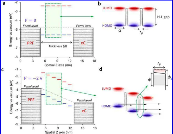
The schematic of Figure 8a depicts several elements of the proposed mechanism for multistep tunneling transport. Six pairs of HOMO and LUMO states represent the molecular layer, where each orbital may be localized on one or at most two FL molecules, with a localization length of α shown in
Figure 8b. These orbitals are broadened by disorder, electronic coupling, and vibrational states and are separated by a distance rij, resulting in a tunneling barrier with a height equal to the H-L gap and width equal to rij. Note that the orbital energies near the electrode interfaces are perturbed by electronic coupling with the contacts and may shift and broaden relative to the electrode Fermi level by partial charge transfer to the electrodes, often called a “vacuum level shift”.15,52−54Provided “injection” of carriers is fast relative to bulk transport, the observed current is limited by tunneling through the H-L barrier, and tunneling may occur across more than one H-L gap (as shown inFigure 8d). In an applied electric field (Figure 8c− d), the barrier height is reduced, as shown in the inset ofFigure 8d. Under this model, the important factors controlling the current density are the H-L gap in the “bulk” molecular layer, rij, α, and the number of steps required to transit across layer thickness d. The relative energies of the orbitals and the electrode Fermi level are not relevant to transport, since the rate-limiting step is tunneling across the H-L barrier within the molecular layer interior. A transport mechanism controlled by the molecular layer properties rather than the contacts, as we propose here, may be an advantage of aromatic carbon contacts such as sp2 hybridized carbon or graphene. Several recent reports using carbon-based molecular junctions have identified attractive electronic properties and/or high stability when molecules are covalently bonded to carbon contacts.41,55−57
Finally, the current multistep tunneling model depends on “sites” separated by a barrier determined by the H-L gap in the film interior and assumes relatively rapid carrier transport at the carbon electrode interfaces due to strong electronic coupling Figure 8. (a) Energy level diagram at zero bias for a FL junction with six pairs of localized HOMO and LUMO states, using free molecule DFT energies and a PPF Fermi level of −4.8 eV. (b) Magnification of three paired H-L states; α and rijare the localization length and tunneling distance between two neighboring states. (c) The same diagram as panel a for V = −2 V bias (PPF negative), assuming a linear potential profile through the molecular layer. (d) Magnification of panel c, with inset showing the tunneling barrier with height ϕ0at zero bias and ϕ with bias applied. Arrows indicate possible tunneling paths for electrons.
between the graphitic π system and the aromatic molecules. At the simplest limit, an electron moves from the HOMO of the molecule at an electrode interface into the electrode, thus creating a hole which is filled by tunneling from a nearby HOMO through the H-L barrier. Depending on the time scale, the hole could result in reorganization, leading to polaron formation and a mechanism similar to “polaron tunneling” proposed recently by Taherinia et al.29 The small activation energies observed in the current devices, particularly at low T, are evidence against reorganization to a polaron being a prerequisite for transport and are more consistent with a multistep tunneling model such as that presented inFigure 8. Current research is focused on confirming the importance of the H-L gap to determine conductance in carbon-bases molecular junctions and investigating the generality of observation that carrier injection is not rate limiting.
CONCLUSIONS
Charge transport in aromatic carbon/molecule/carbon molec-ular junctions is strongly affected both by electronic coupling between the electrodes and the molecules and by relatively weak coupling between oligomer subunits. As a result, efficient transport does not correlate with the energies of molecular orbitals relative to the electrode Fermi levels, but is directly controlled by the HOMO−LUMO energy gap in the molecular layer interior. The factors of >1000 differences in conductance with variations in molecular structure observed for d = 10 nm result from changes in the H-L gap indicated directly by UV− vis absorption of molecular layers bonded to graphitic carbon. The unusual linearity of ln J with V1/2 observed for all four molecules is consistent with lowering of the H-L tunneling barrier in the applied electric field, and the weak temperature dependence is expected for a multistep, sequential tunneling mechanism. The important parameters controlling electron transport are the H-L energy gap within the molecular layer, the tunneling distance between molecular orbitals (rji), the localization length (α), and the number of steps required to traverse the molecular layer. At least for the case of strong electronic coupling between carbon electrodes and aromatic molecular layers, the findings provide useful guidance for rational design of molecular electronic devices with desired electronic behaviors.
METHODS
Fabrication of junctions on pyrolyzed photoresist film (PPF) was conducted as described previously, with electron-beam deposited carbon (eC) and Au top contacts.19,25Junctions are designated with
subscripts in nm on the “stack” of contacts and molecular layers, viz. PPF/FL5.0/eC10/Au20 (FL5.0 designates a FL oligomer with d = 5.0 nm). The same junction structure was used in all cases, with variation only of the identity and thickness of the molecular layer, and the junction area was 0.00125 cm2 (250 × 500 μm). FL deposition by reduction of diazonium reagents is radical-mediated, hence the films are covalently bonded to the PPF and between FL subunits, with partial ordering along the axis perpendicular to the PPF. The thickness of the molecular layer was controlled by the scan range of the electrochemical reduction using the conditions listed in Supporting Informationsection 1 and was validated by AFM “scratching.”58All
electrical measurements were done with a Keithley 2602 source-meter in 4-wire configuration and custom program to have dynamic NPLC over a wide range of applied voltage bias. Additional experimental details regarding fabrication and electrical measurements are provided inSupporting Informationsections 1 and 2.
ASSOCIATED CONTENT
*
S Supporting InformationThe Supporting Information is available free of charge on the
ACS Publications websiteat DOI:10.1021/acsnano.7b00597. Junction fabrication details, absorption spectra, temper-ature results, and additional JV curves and statistics (PDF)
AUTHOR INFORMATION
Corresponding Author
*E-mail: [email protected].
ORCID
Amin Morteza Najarian:0000-0002-0455-0451
Richard L. McCreery:0000-0002-1320-4331
Notes
The authors declare no competing financial interest. ACKNOWLEDGMENTS
This work was supported by the University of Alberta, the National Research Council of Canada, the Natural Science and Engineering Research Council of Canada, and Alberta Innovates. The authors thank Dr. A. J. Bergren at the National Institute for Nanotechnology and Prof. J.-C. Lacroix at the University of Paris for informative conversations and the BTB amine precursor.
REFERENCES
(1) Su, T. A.; Neupane, M.; Steigerwald, M. L.; Venkataraman, L.; Nuckolls, C. Chemical Principles of Single-Molecule Electronics. Nat. Rev. Mater. 2016, 1, 16002.
(2) Metzger, R. M. Unimolecular Electronics. Chem. Rev. 2015, 115, 5056−5115.
(3) Xiang, D.; Wang, X.; Jia, C.; Lee, T.; Guo, X. Molecular-Scale Electronics: From Concept to Function. Chem. Rev. 2016, 116, 4318− 4440.
(4) McCreery, R.; Yan, H.; Bergren, A. J. A Critical Perspective on Molecular Electronic Junctions: There is Plenty of Room in the Middle. Phys. Chem. Chem. Phys. 2013, 15, 1065−1081.
(5) Moth-Poulsen, K.; Bjornholm, T. Molecular Electronics With Single Molecules in Solid-State Devices. Nat. Nanotechnol. 2009, 4, 551−556.
(6) McCreery, R. L. The Merger of Electrochemistry and Molecular Electronics. Chem. Rec. 2012, 12, 149−163.
(7) Reus, W. F.; Nijhuis, C. A.; Barber, J. R.; Thuo, M. M.; Tricard, S.; Whitesides, G. M. Statistical Tools for Analyzing Measurements of Charge Transport. J. Phys. Chem. C 2012, 116, 6714−6733.
(8) Chiechi, R. C.; Weiss, E. A.; Dickey, M. D.; Whitesides, G. M. Eutectic Gallium-Indium (EGaIn): A Moldable Liquid Metal for Electrical Characterization of Self-Assembled Monolayers. Angew. Chem., Int. Ed. 2008, 47, 142−144.
(9) Akkerman, H. B.; Blom, P. W. M.; de Leeuw, D. M.; de Boer, B. Towards Molecular Electronics with Large-Area Molecular Junctions. Nature 2006, 441, 69.
(10) Bonifas, A. P.; McCreery, R. L. ″Soft″ Au, Pt and Cu Contacts for Molecular Junctions Through Surface-Diffusion-Mediated Depo-sition. Nat. Nanotechnol. 2010, 5, 612−617.
(11) Finklea, H. O., Electrochemistry of Organized Monolayers of Thiols and Related Molecules on Electrodes. In Electroanalytical Chemistry; Bard, A. J., Ed.; Dekker: New York, 1996; Vol. 19, pp 109− 335.
(12) Creager, S.; Yu, C. J.; Bamdad, C.; O’Connor, S.; MacLean, T.; Lam, E.; Chong, Y.; Olsen, G. T.; Luo, J.; Gozin, M.; Kayyem, J. F. Electron Transfer at Electrodes through Conjugated ″Molecular Wire″ Bridges. J. Am. Chem. Soc. 1999, 121, 1059−1064.
(13) Bergren, A. J.; McCreery, R. L.; Stoyanov, S. R.; Gusarov, S.; Kovalenko, A. Electronic Characteristics and Charge Transport Mechanisms for Large Area Aromatic Molecular Junctions. J. Phys. Chem. C 2010, 114, 15806−15815.
(14) He, J.; Chen, F.; Li, J.; Sankey, O.; Terazono, Y.; Herroro, C.; Gust, D.; Moore, T.; Moore, A. L.; Lindsay, S. M. Electronic Decay Constant of Carotenoid Polyenes From Single-Molecule Measure-ments. J. Am. Chem. Soc. 2005, 127, 1384−1385.
(15) Sayed, S. Y.; Fereiro, J. A.; Yan, H.; McCreery, R. L.; Bergren, A. J. Charge Transport in Molecular Electronic Junctions: Compression of the Molecular Tunnel Barrier in the Strong Coupling Regime. Proc. Natl. Acad. Sci. U. S. A. 2012, 109, 11498−11503.
(16) Sedghi, G.; Esdaile, L. J.; Anderson, H. L.; Martin, S.; Bethell, D.; Higgins, S. J.; Nichols, R. J. Comparison of the Conductance of Three Types of Porphyrin-Based Molecular Wires: β,meso,β-Fused Tapes, meso-Butadiyne-Linked and Twisted meso-meso Linked Oligomers. Adv. Mater. 2012, 24, 653−657.
(17) Sedghi, G.; Garcia-Suarez, V. M.; Esdaile, L. J.; Anderson, H. L.; Lambert, C. J.; Martin, S.; Bethell, D.; Higgins, S. J.; Elliott, M.; Bennett, N.; Macdonald, J. E.; Nichols, R. J. Long-Range Electron Tunnelling in Oligo-Porphyrin Molecular Wires. Nat. Nanotechnol. 2011, 6, 517−523.
(18) Tuccitto, N.; Ferri, V.; Cavazzini, M.; Quici, S.; Zhavnerko, G.; Licciardello, A.; Rampi, M. A. Highly Conductive 40-nm-long Molecular Wires Assembled by Stepwise Incorporation of Metal Centres. Nat. Mater. 2009, 8, 41−46.
(19) Yan, H.; Bergren, A. J.; McCreery, R. L. All-Carbon Molecular Tunnel Junctions. J. Am. Chem. Soc. 2011, 133, 19168−19177.
(20) Luo, L.; Choi, S. H.; Frisbie, C. D. Probing Hopping Conduction in Conjugated Molecular Wires Connected to Metal Electrode. Chem. Mater. 2011, 23, 631−645.
(21) Choi, S. H.; Kim, B.; Frisbie, C. D. Electrical Resistance of Long Conjugated Molecular Wires. Science 2008, 320, 1482−1486.
(22) Lu, Q.; Liu, K.; Zhang, H.; Du, Z.; Wang, X.; Wang, F. From Tunneling to Hopping: A Comprehensive Investigation of Charge Transport Mechanism in Molecular Junctions Based on Oligo(p-phenylene ethynylene)s. ACS Nano 2009, 3, 3861−3868.
(23) Amdursky, N.; Marchak, D.; Sepunaru, L.; Pecht, I.; Sheves, M.; Cahen, D. Electronic Transport via Proteins. Adv. Mater. 2014, 26, 7142−7161.
(24) Lee, S. K.; Yamada, R.; Tanaka, S.; Chang, G. S.; Asai, Y.; Tada, H. Universal Temperature Crossover Behavior of Electrical Con-ductance in a Single Oligothiophene Molecular Wire. ACS Nano 2012, 6, 5078−5082.
(25) Yan, H.; Bergren, A. J.; McCreery, R.; Della Rocca, M. L.; Martin, P.; Lafarge, P.; Lacroix, J. C. Activationless Charge Transport Across 4.5 to 22 nm in Molecular Electronic Junctions. Proc. Natl. Acad. Sci. U. S. A. 2013, 110, 5326−5330.
(26) Xie, Z.; Bâldea, I.; Smith, C. E.; Wu, Y.; Frisbie, C. D. Experimental and Theoretical Analysis of Nanotransport in Oligophenylene Dithiol Junctions as a Function of Molecular Length and Contact Work Function. ACS Nano 2015, 9, 8022−8036.
(27) Baldea, I.; Xie, Z.; Frisbie, C. D. Uncovering a Law of Corresponding States for Electron Tunneling in Molecular Junctions. Nanoscale 2015, 7, 10465−10471.
(28) Luo, L.; Balhorn, L.; Vlaisavljevich, B.; Ma, D.; Gagliardi, L.; Frisbie, C. D. Hopping Transport and Rectifying Behavior in Long Donor−Acceptor Molecular Wires. J. Phys. Chem. C 2014, 118, 26485−26497.
(29) Taherinia, D.; Smith, C. E.; Ghosh, S.; Odoh, S. O.; Balhorn, L.; Gagliardi, L.; Cramer, C. J.; Frisbie, C. D. Charge Transport in 4 nm Molecular Wires with Interrupted Conjugation: Combined Exper-imental and Computational Evidence for Thermally Assisted Polaron Tunneling. ACS Nano 2016, 10, 4372−4383.
(30) Kondratenko, M.; Stoyanov, S. R.; Gusarov, S.; Kovalenko, A.; McCreery, R. L. Theoretical Modeling of Tunneling Barriers in Carbon-Based Molecular Electronic Junctions. J. Phys. Chem. C 2015, 119, 11286−11295.
(31) McCreery, R. L. Effects of Electronic Coupling and Electrostatic Potential on Charge Transport in Carbon-Based Molecular Electronic Junctions. Beilstein J. Nanotechnol. 2016, 7, 32−46.
(32) Gibbs, J.; Otero de la Roza, A.; Bergren, A. J.; DiLabio, G. A. Interpretation of Molecular Device Transport Calculation. Can. J. Chem. 2016, 94, 1022−1027.
(33) Sze, S. M. Physics of Semiconductor Devices, 2nd ed; Wiley: New York, 1981.
(34) Ivashenko, O.; Bergren, A. J.; McCreery, R. L. Monitoring of Energy Conservation and Losses in Molecular Junctions Through Characterization of Light Emission. Adv. Electron. Mater. 2016, 2, 1600351.
(35) Donner, S.; Li, H. W.; Yeung, E. S.; Porter, M. D. Fabrication of Optically Transparent Carbon Electrodes by the Pyrolysis of Photoresist Films: Approach to Single-Molecule Spectroelectrochem-istry. Anal. Chem. 2006, 78, 2816−2822.
(36) Tian, H.; Bergren, A. J.; McCreery, R. L. UltravioletVisible Spectroelectrochemistry of Chemisorbed Molecular Layers on Optically Transparent Carbon Electrodes. Appl. Spectrosc. 2007, 61, 1246−1253.
(37) Fereiro, J. A.; Kondratenko, M.; Bergren, A. J.; McCreery, R. L. Internal Photoemission in Molecular Junctions: Parameters for Interfacial Barrier Determinations. J. Am. Chem. Soc. 2015, 137, 1296−1304.
(38) Ortiz, R. P.; Facchetti, A.; Marks, T. J. High-k Organic, Inorganic, and Hybrid Dielectrics for Low-Voltage Organic Field-Effect Transistors. Chem. Rev. 2010, 110, 205−239.
(39) Tsuda, A.; Osuka, A. Fully Conjugated Porphyrin Tapes with Electronic Absorption Bands That Reach into Infrared. Science 2001, 293, 79−82.
(40) Choi, S. H.; Risko, C.; Delgado, M. C. R.; Kim, B.; Bredas, J.-L.; Frisbie, C. D. Transition from Tunneling to Hopping Transport in Long, Conjugated Oligo-imine Wires Connected to Metals. J. Am. Chem. Soc. 2010, 132, 4358−4368.
(41) Morteza Najarian, A.; Szeto, B.; Tefashe, U. M.; McCreery, R. L. Robust All-Carbon Molecular Junctions on Flexible or Semi-Transparent Substrates Using “Process-Friendly” Fabrication. ACS Nano 2016, 10, 8918−8928.
(42) Yan, H.; McCreery, R. L. Anomalous Tunneling in Carbon/ Alkane/TiO2/Gold Molecular Electronic Junctions: Energy Level Alignment at the Metal/Semiconductor Interface. ACS Appl. Mater. Interfaces 2009, 1, 443−451.
(43) Roberts, G. G.; Apsley, N.; Munn, R. W. Temperature Dependent Electronic Conduction in Semiconductors. Phys. Rep. 1980, 60, 59−150.
(44) Stallinga, P. Electronic Transport in Organic Materials: Comparison of Band Theory with Percolation/(Variable Range) Hopping Theory. Adv. Mater. 2011, 23, 3356−3362.
(45) Tessler, N.; Preezant, Y.; Rappaport, N.; Roichman, Y. Charge Transport in Disordered Organic Materials and Its Relevance to Thin-Film Devices: A Tutorial Review. Adv. Mater. 2009, 21, 2741−2761.
(46) Lee, P. A.; Ramakrishnan, T. Disordered Electronic Systems. Rev. Mod. Phys. 1985, 57, 287.
(47) Baranovskii, S.; Rubel, O., Charge Transport in Disordered Materials. In Springer Handbook of Electronic and Photonic Materials; Springer: New York, 2006; pp 161−186.
(48) Roberts, G. G.; Polanco, J. I. Thermally Assisted Tunnelling in Dielectric Films. phys. status solidi A 1970, 1, 409−420.
(49) Riben, A. R.; Feucht, D. L. Electrical Transport in nGe-pGaAs Heterojunctions. Int. J. Electron. 1966, 20, 583−599.
(50) Martinuzzi, S.; Mallem, O. Dark-Current Conduction Processes in CdS−Cu2S Thin-Film Photocells. phys. status solidi A 1973, 16, 339−344.
(51) Karipidou, Z.; Branchi, B.; Sarpasan, M.; Knorr, N.; Rodin, V.; Friederich, P.; Neumann, T.; Meded, V.; Rosselli, S.; Nelles, G.; Wenzel, W.; Rampi, M. A.; von Wrochem, F. Ultrarobust Thin-Film Devices from Self-Assembled Metal−Terpyridine Oligomers. Adv. Mater. 2016, 28, 3473−3480.
(52) Braun, S.; Salaneck, W. R.; Fahlman, M. Energy-Level Alignment at Organic/Metal and Organic/Organic Interfaces. Adv. Mater. 2009, 21, 1450−1472.
(53) Hwang, J.; Wan, A.; Kahn, A. Energetics of Metal−Organic Interfaces: New Experiments and Assessment of the Field. Mater. Sci. Eng., R 2009, 64, 1−31.
(54) Vilan, A.; Yaffe, O.; Biller, A.; Salomon, A.; Kahn, A.; Cahen, D. Molecules on Si: Electronics with Chemistry. Adv. Mater. 2010, 22, 140−159.
(55) Jia, C.; Migliore, A.; Xin, N.; Huang, S.; Wang, J.; Yang, Q.; Wang, S.; Chen, H.; Wang, D.; Feng, B.; Liu, Z.; Zhang, G.; Qu, D.-H.; Tian, H.; Ratner, M. A.; Xu, H. Q.; Nitzan, A.; Guo, X. Covalently Bonded Single-Molecule Junctions With Stable and Reversible Photoswitched Conductivity. Science 2016, 352, 1443−1445.
(56) Jia, C.; Ma, B.; Xin, N.; Guo, X. Carbon Electrode−Molecule Junctions: A Reliable Platform for Molecular Electronics. Acc. Chem. Res. 2015, 48, 2565−2575.
(57) Kim, D.; Jeong, H.; Lee, H.; Hwang, W.-T. T.; Wolf, J.; Scheer, E.; Huhn, T.; Jeong, H.; Lee, T. Flexible Molecular-Scale Electronic Devices Composed of Diarylethene Photoswitching Molecules. Adv. Mater. 2014, 26, 3968−3973.
(58) Anariba, F.; DuVall, S. H.; McCreery, R. L. Mono- and Multilayer Formation by Diazonium Reduction on Carbon Surfaces Monitored with Atomic Force Microscopy ″Scratching″. Anal. Chem. 2003, 75, 3837−3844.