Edible Photonic Crystals Tunable Within the Visible Regime
by
Xavier Gonzslez
Submitted to the Department of Materials Science and Engineering in Partial Fulfillment of the Requirements for the
Degree of Bachelor of Science
at the
Massachusetts Institute of Technology June 2010 MASSACHUSETTS INSTITUTE OF TECHNOLOGY
JUL 1
0
2017
LIBRARIES
ARCHIVES
2010 Xavier GonzslezAll rights reserved
The author hereby grants to MIT permission to reproduce and to
distribute publicly paper and electronic copies of this thesis document in whole or in part in any medium now known or hereafter created.
Signature of Aut
Ce0rti fie b
Signature redacted
h o r.. ...
Department of Materials Science and Engineering
May 13, 2010
Signature redacted
y ... ...
Edwin L. Thomas Department Head and Morris Cohen Professor of Materials Science and Engineering Thesis Supervisor
Signature redacted
A ccepted by ... Lionel C. Kimerling Chairman, Undergraduate Committee
Edible Photonic Crystals Tunable Within the Visible Regime
by
Xavier Gonz6lez
Submitted to the Department of Materials Science and Engineering on May 13, 2010 in Partial Fulfillment of the
Requirements for the Degree of Bachelor of Science in Materials Science and Engineering
ABSTRACT
An experimental study was performed to design and fabricate an edible photonic crystal made of alternating layers of food grade titanium dioxide and agar that is able to selectively reflect wavelengths of light within the visible spectrum and allow for dynamic color changes through the tuning mechanism of swelling its agar layers with the addition of edible solvents. After doing a literature search to discover which materials were available to create this edible photonic structure, a trial and error process was conducted using deposition and film thickness characterization techniques to optimize the physical and optical characteristics of the layers composing the photonic structure. The materials selected for the layers in the structure yield a high refractive index contrast, which allows for high reflectivity with a reduced amount of total layers. The multilayer stack can be designed to reflect particular wavelengths by selecting the thickness of the layers accordingly.
Thin film characterization took place through the use of profilometry, ellipsometry, and atomic force microscopy. The feasibility and practicality of two manufacturing techniques, spincoating and RF-sputtering, were analyzed in the process of learning how to assemble an edible multilayer stack for molecular gastronomy applications.
Thesis Supervisor: Edwin L. Thomas
BIOGRAPHICAL NOTE
Xavier Gonzalez was born and raised in Miami, Florida and is proud of his Nicaraguan heritage. He began his studies at MIT in the fall of 2006 working towards a bachelor's degree in Materials Science and Engineering. Since then, he has gone on to enter various innovation competitions such as the IDEAS
competition and won 2nd place at the MIT and Dow Chemical Materials
Engineering Contest. With a grant from the Public Service Center at MIT he went to Nicaragua in the summer of 2007 to build novel multi-phase biogas digesters. He performed research in the Thomas Group at MIT on the thermochromic properties of photonic gels under the supervision of Dr. Joseph J. Walish and Professor Edwin L. Thomas. He was then inspired by the convergence of science, art, and gastronomy when he learned of the work of Ferran Adrib at El Bulli and felt compelled to integrate photonics to the world of molecular gastronomy. He went on to be the co-instructor for the Food Science and Design course offered at MIT in the spring semester of 2010 and continues to develop gastronomic innovations.
ACKNOWLEDGEMENTS
I would like to thank Professor Edwin Thomas and Dr. Joseph Walish for their support and guidance in this project. Through them I have grown as a science researcher these past few years and have become familiar with many experimental techniques. I would like to thank Professor Rubner for his help at the onset of the project. I would also like to thank Professor Swager's and Professor Ross' groups for allowing me access to their labs. I appreciate the patience of Professor Ross' group members, Kevin Gotrik and Chunghee Nam who dedicated many hours of their time to teach me how to operate their sputtering machine. A special thanks to Jeffrey Kuna for always providing me with insight and motivating me throughout the course of my project.
I would not have been able to complete this project without the support of my good friend Corey Kubber. I am sure we will always remember how we kept each other alive throughout our courses at MIT, resonating positive energy to each other, and how we always "pulled through" even when things seemed impossible to accomplish.
I would not have been able to complete my studies at MIT without the support of the love of my life, Leonor Barrios, my beloved mother, my brothers and sisters, Tia Frida, Guiti, my crazy niece, Vanessita, and my good friends Ali Osman, Serdar Karatekin, Thomas Santamaria, Alejandro Ojeda, Juan Manjarres, Jorge Sanchez, Andres Chong-qui, Juan Molina, Paulina Mustafa, and Ivan Bustillo.
TABLE OF CONTENTS A B S T R A C T ... 2 BIOGRAPHICAL NOTE ... 3 ACKNOWLEDGEMENTS ... 3 TABLE OF CONTENTS ... 4 LIST OF FIGURES... 5 Chapter 1 INTRODUCTION ... 7 1.1 INTRODUCTORY REMARKS... 7 1 .2 PRIO R A RT... 8 Chapter 2 PHOTONICS... 10 2.1 SOURCES OF COLOR ... 10
2.2 ONE-DIMENSIONAL PHOTONIC CRYSTALS ... 12
2.3 DESIGN OF MULTILAYER STACK ... 13
Chapter 3 MATERIALS ... 18
3 .1 A G A R ... ... 1 8 3 .2 T ITA N IA ... 19
Chapter 4 EXPERIMENTAL TECHNIQUES... 21
4 .1 INTRO D UCTIO N ... 2 1 4 .2 S PINCOATING ... 2 1 4.3 PROFILOMETRY... 23
4.4 OPTIMIZING THE CHARACTERISTICS OF THE AGAR FILM... 25
4.5 OPTIMIZING THE CHARACTERISTICS OF THE TITANIA FILM... 30
4.6 DETERMINING THE SIZE DISTRIBUTION OF TITANIA PARTICLES... 31
4.7 RF-SPUTTERING ... 34
4.8 ATOMIC FORCE MICROSCOPY ... 37
4.9 ELLIPSOMETRY ... 40
Chapter 5 TUNABILITY OF THE PHOTONIC STUCTURE... 46
5.1 SWELLING OF THE AGAR LAYER ... 46
5.2 TUNING THE STRUCTURE ON DEMAND... 46
Chapter 6 CONCLUSIONS AND FUTURE WORK ... 48
R E FE R E N C E S ... 5 0
LIST OF FIGURES
Figure 1: Molecular structure of an anthocyanin and a specific kind of 10
anthocyanin known as cyanidin.
Figure 2: One-dimensional photonic crystal showing alternating layers of 13
agar and titania with their corresponding target layer thickness and refractive index.
Figure 3: The peak reflectivity for various refractive index contrasts is 14 shown. Each curve is for a different number of total layers, 2N, in the
multilayer stack. Higher refractive index contrast allows for higher reflectivities to be reached with a reduced number of total layers.
Figure 4: Reflectivity spectra as a function of wavelength for various 15
refractive index contrasts.
Figure 5: A one-dimensional photonic crystal designed to reflect red 16
light.
Figure 6: a) Molecular structure of agarose polymer. b) 0.08 wt.% 19
agarose viscous liquid solution. c) Agarose solid gel network with junctions.
Figure 7: The spincoating process: apply the solvent solution onto the 22 substrate, then allow this sample to rapidly rotate, removing any excess
solution off the edges. The solution will then dry forming a film on the substrate. Repeat the process to create a multilayer structure.
Figure 8: Diagram showing the setup for scanning the surface of a film 23
using a profilometer. As the stylus moves across the sample it collects information on the topography of the film. The inset shows how the stylus tip can measure the difference in elevation between the film and the
sample, which can be then used to determine the film's thickness.
Figure 9: Photograph of an agar film on a silicon wafer substrate scored 24 using a razorblade.
Figure 10: Profilometry scan of a 2% agar in water film spincoated at 25 4000 RPM. The scan length for this run was 300 microns. The thickness of
the dry film was determined by getting the difference between the average height of the film and the average height of the substrate, which for this sample is about 100 nm.
Figure 11: Variation in film thickness with increasing rotation speed on 26 3% spincoated agar films, displaying an exponential decay relationship.
Figure 12: Profilometry scan for 0.5% agar film spincoated at 4000 RPM. 29
Scan length was 1020 microns with a speed of 50 microns per second.
Figure 13: Profilometry scan for 1% agar film spincoated at 2000 RPM. 29
Figure 14: Size distribution of titania particles obtained using the 33
Dynamic Light Scattering technique. The graph shows the amount of particles of a certain diameter while the accompanying table displays the normalized values that correspond to the data in the graph.
Figure 15: Schematic of RF-Sputtering technique. 34
Figure 16: a) Photograph of clean silicon wafer substrate before 36
sputtering. b) Photograph of 30 minute sputtered titania film on silicon substrate displaying yellow tint, confirming successful deposition of the
film.
Figure 17: Unsuccessful profilometry scan of titania sputtered for 15.5 37 minutes.
Figure 18: Schematic of atomic force microscopy operation mechanism. 39
Figure 19: AFM images of titania sample sputtered for 15.5 minutes. Left 40 image shows the boundary between the titania film and silicon wafer
substrate (after peeling off the tape). Right image shows the topography of the titania film (notice the darker circular features referred to as pores).
Figure 20: Orthogonal waves combine to form elliptical polarization. 41
Figure 21: Schematic of ellipsometry operation mechanism showing how 42 incoming linearly polarized light is reflected off the surface of a sample,
and the change in polarization of light is measured to verify the response of the sample.
Figure 22: Graph of the real (n) and imaginary (k) components of the 43 complex refractive index. The refractive index of the titania film can be
approximated to be 2.2 for the visible regime. The extinction coefficient,
k, is approximately zero throughout the entire visible regime, meaning
that there is very low absorption in the film.
Figure 23: Schematic showing the shortening of the wavelength of light 44 (reduction in phase velocity with constant frequency) as it goes through
media with higher index of refraction. Here, nj > n2, and film 1 is an absorbing film, so there is also a reduction in intensity as the light is absorbed during propagation through film 1 before it reaches the transparent second film.
Figure 24: A good fit between the generated model and the experimental 45 data curves. This validates the calculation of the optical constants, n and
k, as well as the thickness of the titania sample.
Figure 25: Profilometry scan for 1% TiO2 film spincoated at 2000 RPM. 53 Scan length was 1051 microns with a speed of 50 microns per second.
Figure 26: Profilometry scan for 5% TiO2 film spincoated at 1000 RPM. 53
Scan length was 611 microns with a speed of 50 microns per second.
Figure 27: 3D roughness for 5% TiC2 film spincoated at 1000 RPM. Scan 54
length was about 1000 microns with a speed of 50 microns per second.
CHAPTER 1:
INTRODUCTION1.1: INTRODUCTORY REMARKS
The field of molecular gastronomy, a form of food science applied to haute cuisine that studies the physical and chemical processes that take place while cooking, has become increasingly popular over the last few years partly due to the breakthroughs that have come out of premier, avant-garde restaurants such as El Bulli and The Fat Duck. These include the making of culinary foams by Ferran Adrib (Head Chef of El Bulli) as well as Heston Blumenthal's (Head Chef of The Fat Duck) famous tea that is hot and cold in the'same dish [1]. This special tea is made possible through the use of gelling agents that reduce the rate of mixing between both solutions. Blumenthal also cooks meats under vacuum through thermal convection using plastic, sealed bags in heated water in order to achieve a consistent thermal profile throughout thick steaks, resulting in steaks that are not charred on the surface and pink in the center, but consistent throughout [1]. As innovative as these restaurants are, however, there always -exists a need for new ideas and constant evolution of their work. Because these food innovations rely heavily on materials science concepts such as the multiple phases of matter, and the structure, thermal properties, and bonding present in various edible materials, chefs need the help of materials scientists to stay at the cutting edge of their
field. This project aims to merge photonics and gastronomy in order to bring a revolutionary way of producing dynamic color changes in food through the design and fabrication of an edible one-dimensional photonic crystal (a multi-layer stack of alternating layers of dielectric materials that are periodic in one direction) that is tunable within the visible regime.
1.2: PRIOR ART
The idea of "edible photonics" has been inspired by the recent work done in the lab of Professor Edwin Thomas in highly tunable photonic gels consisting of poly(styrene- block 2-vinylpyridine) as well as the earlier work of Dr. Heid-i Burch in conjunction with Professors Edwin Thomas, John Joannopoulos, and Yoel Fink in edible photonic crystals. Dr. Burch's work dealt with a materials system or dielectric structure consisting of biocompatible materials (can come in contact with at least one part of the body without causing. significant health hazards) that have different indices of refraction and that are assembled in order to have a photonic band gap in one or more directions [2]. The product would have the ability to reflect light at a predetermined range of frequencies and be engineered to exhibit photonic band gaps that are broad or narrow and centered on various parts of the spectrum, including the ultraviolet, visible infrared, and even longer wavelengths. The applications of the product include edible reflectors that could impart a particular color on food, heat shields that minimize heat losses, and the ability to serve as an ultraviolet
protection layer. Part of the motivation for this project comes from the novelty of using photonic structures not just to produce vivid colors in food, but to reversibly change these colors on demand with response to stimuli such as temperature gradients and the addition of solutions; something that has not been done before in the world of gastronomy. Some of the most notable attempts to change the color of food in order to enhance a diner's experience were made by Juan Marie Arzak and his daughter, Elena Arzak, who currently run the renowned Restaurante Arzak in Spain's Basque Country. They have made a dish in which hot broth is poured over a thin slice of squid ink gelatin, melting the gelatin and therefore changing the color of the broth before the diner's eyes (an irreversible color change brought on by the mixing of the two materials). The same technique has been used over pumpkin ravioli (again, an irreversible color caused by mixing). Elena Arzak has gone on to explore the use of color as a tool of innovation on the plate by experimenting with sodium bicarbonate (mildly alkaline in aqueous solutions) to change the color of red cabbage broth and sauces [3]. This technique can be reversible due to the acid/base reactions that take place. This is due to the susceptibility of the cyanidin molecule (an anthocyanin found in red cabbage) to pH changes, which makes the molecule change its structure, causing a change in the wavelengths of lights it absorbs, and thereby changing the color that the diner sees in the cabbage broth or sauce when
sodium bicarbonate or acetic acid are added [4]. The molecular structure of cyanidin and anthocyanin can be found in Figure 1.
ON
Aent renl r Cyan d an
Umv -IWwso 9e 4T. of A-0 auhsca~ ir~emba
Figure 1: Molecular structure of an anthocyanin and a specific kind of anthocyanin
known as cyaniding.
Source: http://www.webexhibits.org/causesofcolor/7G.html
CHAPTER 2: PHOTONICS
2.1: SOURCES OF COLOR
There are various mechanisms that give objects their color. When incident light hits an object, the light is either reflected, absorbed, scattered, transmitted, or a combination of these. Reflection is the change in direction of a light wave at an interface between two media (i.e. air and the object). In other words, when light hits an object, the lights bounces back to the air with the same angle which it hit the surface of the object (specular reflection). Mirrors are a good example of specular reflectors. Transmission is when light is able to penetrate through the medium and
goes straight through, into the air. Absorbance occurs when the photons of the incident light get absorbed by the medium they impact instead of being reflected at the surface. But there are times when the incident light is not completely reflected, absorbed, or transmitted and instead scattered. This is like a diffused reflection where the incident light deviates from a straight trajectory because of non-uniformities in the medium through which it is passing. The color one views in an object is mostly due to which wavelengths of light that object absorbs the most (which determines what wavelengths of light the object reflects and hits the eyes). Also, the wavelengths of light that get scattered most by a material influence its color. For example, a red t-shirt has its color because it scatters wavelengths of light in approximately the 635-700 nm range at higher intensities than it does for the rest of the wavelengths in the visible regime of the electromagnetic spectrum and absorbs the wavelengths corresponding to orange, yellow, green, blue, indigo, and violet light (the remainder of the visible spectrum, 380-635 nm). Likewise, if the object scatters all wavelengths then it will appear to be white. However, if it absorbs all wavelengths then it will appear to be black. Yet another form by which objects exhibit color is due to structural features that give color to objects through interference effects [5]. These structural features are often on the surface of the object and take the form of gratings or
example, structural spacing patterns are responsible for the blue or green color of birds' feathers [6]. When there are variations in the pattern's spacing, it gives rise to iridescence, where the color changes depending on the viewing angle, as seen in peacock's feathers and soap bubbles.
Furthermore, reflectors of constant spacing are also angular dependent. 2.2: ONE-DIMENSIONAL PHOTONIC CRYSTALS
This project, however, aims to achieve these color-changing effects via the use of one-dimensional photonic crystal structures made of alternating layers of food grade titanium dioxide and agar which can have the color of light they reflect tuned by the swelling of the agar layer through rehydration as explained in Chapter 5 (See Figure 2). Photonic crystals are periodic optical structures that consist of alternating layers of
materials with different dielectric constants that reflect different
wavelengths of light depending on: the thickness of the layers, the angle of incident light, and the index of refraction of each layer [5]. The ones being used for this project are considered to be one-dimensional photonic crystals because the dielectric is only periodic in one direction. Because of this periodicity in refractive index, interference effects arise which prevent (or partially prevent) certain modes of light in defined directions [6]. A photonic band gap is an energy range (and corresponding wavelength range) of light that is not absorbed by or propagated through a material. However, for that energy range of light to be considered a complete
photonic band gap of a material, it must be prohibited from propagating in
the material for all directions and polarizations. For the case where only
some directions and polarizations are prohibited, the term stop band is
used. These can be considered to be partial band gaps.
agar (100 nm, n = 1.3)
titania (50 nm, n = 2.2)
Figure 2: One-dimensional photonic crystal showing alternating layers of agar and
titania with their corresponding target layer thickness and refractive index.
2.3: DESIGN OF MULTILAYER STACK
These multilayer films can be designed to reflect light within the
visible regime by engineering certain properties of the individual layers.
For example, when choosing which material to use for each layer it is
useful to consider their indices of refraction. The larger the contrast in
their indices of refraction the fewer number of layers necessary to produce
a strong reflection, making it easier to fabricate these structures. The
material with the higher refractive index in this project is titania (nH=
2.2for the visible regime) while the material with the lower refractive index is
agar (nL=1.3 in various concentrations with water;
nwater=1.
3 3), yielding a
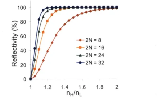
ratio of approximately nH/InL = 1.7, which correlates to high reflectivity with fewer number of layers, N, in the photonic crystal (See Figure 3).
100
801
>' 60 -> 2N= 8 40 -- 2N = 16 +2N = 24 20--
2N = 32 0 1 1.2 1.4 1.6 1.8 2Figure 3: The peak reflectivity for various refractive index contrasts is shown. Each curve is for a different number of total layers, 2N, in the multilayer stack. Higher refractive index contrast allows for higher reflectivities to be reached with a reduced number of total layers.
Source: Yoon, J. Block Copolymer Photonic Crystals: Towards Self-Assembled Active
Optical Elements. Dissertation: Massachusetts Institute of Technology, 2006. Cambridge,
MA.
Likewise, for a given layer thickness (i.e. 100 nm for each layer) and a constant number of total layers (i.e. 2N = 20), one-dimensional photonic crystals that have a higher refractive index contrast between their layers will exhibit higher reflectivity for a broader range of wavelengths (See Figure 4). Holding the same, aforementioned conditions constant, the reflectivity emission peak becomes narrower, shorter, and shifted towards larger wavelengths for multilayer stacks that have a lower
refractive index contrast, as shown by the red curve (nH /fL =
1.5/1.4
= 1.07) in Figure 4.100
- 80 n nL -1.5/1.0 - 60 -1.5/1.1 -1.5/1.2 ( 4 0 -1.5/1.3 2D -1.5/1.4 20-0
300 500 700 900 Wavelength (nm)Figure 4: Reflectivity spectra as a function of wavelength for various refractive index contrasts. The thickness of the layers was held constant at 100 nm and total amount of
layers was kept at 20 for all curves.
Source: Yoon, J. Block Copolymer Photonic Crystals: Towards Self-Assembled Active
Optical Elements. Dissertation: Massachusetts Institute of Technology, 2006. Cambridge,
MA.
The thickness of each layer is another parameter of paramount importance since this, in conjunction with the index of refraction of each layer and the angle of incident light, determines the wavelength of the light that will be reflected for a one-dimensional photonic crystal. The photonic crystal can be designed to reflect a desired wavelength of light with peak intensity (Amax) by choosing the appropriate thickness of the layers of materials with known indices of refraction, as modeled by Equation 1,
{1} Amax=2(din1+d2n2)
where the optical path length of a layer i is the product of its physical thickness (di) and its refractive index (nt) [7]. This relationship exists because light that has been transmitted and refracted through the layers of the photonic crystal is also reflected back at each subsequent layer, which means there exists a wavelength that is equal to half of the optical path length, causing deconstructive interference of that wavelength when it is reflected back. In other words, the characteristic optical path lengths of a photonic crystal cause a certain peak wavelength to be prohibited (canceled) in the material, which is why it becomes reflected with high intensity. It can be stated that the wavelength is diffracted since it cannot be transmitted, and it is instead reflected at the near surface regions (See Figure 5).
nd,
~td,
Figure 5: A one-dimensional photonic crystal designed to reflect red light.
Source: Walish, J.J. Bio-Inpsired Optical Components. Dissertation: Massachusetts Institute of Technology, 2008. Cambridge, MA. (altered from original diagram)
Since the visible regime of the electromagnetic spectrum ranges between 380 nm and 750 nm, the thickness of the layers used in this project range between 50 and 100 nm depending on whether the desired starting color is more on the blue or red end of the spectrum. In addition, it is important to make sure that the individual layers are smooth in order to achieve the photonic effects aforementioned. This is where chemistry and proper processing of the materials being used becomes important.
Furthermore, in order to allow for these structures to be able to dynamically change the color of light they reflect it is necessary to be able to change the index of refraction or thickness of at least one of the layers. One method to tune the color of the light the photonic crystal structure reflects is by swelling and shrinking one of the layers in the structure. With aqueous solvents it is possible to swell one of the layers in the photonic structure, increasing the thickness of the layer as well as the refractive-index contrast, resulting in a red-shift of the light emitted by the photonic structure (discussed in more detail in Chapter 5) [7]. Accordingly, for this project it is necessary to make sure that the two materials being used to make the periodic structure are completely edible.
CHAPTER 3:
MATERIALS3.1: AGAR
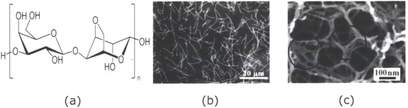
The first of the two materials being used to make the edible multilayer film is agar (refractive index ~1.3 in water solution). Agar in powder form was obtained from Sigma Aldrich. Since its index of refraction is similar to that of water, the refractive index of the agar/water solution is not very dependent on concentration. Agar is a heterogeneous complex mixture of related polysaccharides that have the same backbone chain structure. The main components of that chain are D-galactopyranose and 3,6-anhydro-L-galactopyranose, which alternate through a-(1,4) and
,8-(1,3) linkages [8]. Agar consists primarily of the linear form of the
neutral polymer, agarose (molecular weight is about 120,000 amu), which has the ability to create firm gels (See Figure 6). Agarose gel networks contain double helices that are stabilized by the binding of water molecules inside the double helix. The sulfated polymer, agaropectin, is also another main component of agar. In addition, the charged chains have pyruvic acid bound in ketal form [8]. Some of the properties of this gelatinous substance include a large hysteresis since it melts at 850 C and solidifies between 320 C to 400 C. Furthermore, The melting point of agar solutions does not vary much with concentration. Agar is derived from the cell walls of certain species of red algae in the class Rhodophyceae [8].
This material has been extensively used in Japanese cuisine and has become very popular with the high-end restaurants. It can be used as a thickener for soups, a clarifying agent in brewing, and is essential for giving the proper texture to jellies, ice cream and other Japanese desserts such as anmitsu. But the reason this material was chosen to make up one of the layers of the edible photonic crystal is mainly due to its gelling properties and its ability to tune the color of light reflected by the structure. This is because agar is able to swell up to 3000% its volume from the dehydrated state when water is reintroduced into the system.
OHi OH0
OH
H"
01
(a) (b) (c)
Figure 6: a) Molecular structure of agarose polymer. b) 0.08 wt.% agarose viscous liquid
solution. c) Agarose solid gel network with junctions.
Sources: http://upload.wikimedia.org/wikipedia/commons/2/2b/Agarosepolymere.svg (a)
http://www3.interscience.wiley.com/cg i-bin/fu lltext/ 117861100/PDFSTART (b and c)
3.2: TITANIA
The other material used to construct the edible photonic crystal is food grade titanium dioxide, also known as FG titania. This material occurs naturally in well-known minerals such as rutile, anatase, and brookite but the one that is usually used in food and cosmetic applications is derived
from rutile. This material is most widely used to give objects a white appearance because of its ability to scatter light really well when it is in small particle form. Titania has a very high refractive index (reaching up
to ~,2.6), which allows it to make the products it is applied onto appear
brighter [9]. It can be found in such applications as candy canes, pills and tablets, as well as most toothpastes. This food additive has been assigned an E number (E171), which means that it has been approved for human consumption and use throughout the European Union [10]. The Food and Drug Administration (FDA) regulates color additives used in food and evaluates scientific data and information to ensure that a color additive is safe for its intended purposes. FDA regulation 21 CFR 73.350 provides for the safe use of titanium dioxide coated mica-based pearlescent pigments as color additives (up to 1.25% of the finished product weight for the titania-coated pigments and 1.00% by weight of the food for titania particles) in the following foods: cereals, confections and frostings, gelatin desserts, hard and soft candies, nutritional supplement tablets and gelatin capsules, and chewing gum [11]. The primary reason this material is being used in this project is because its high refractive index offers high index contrast between the two alternating layers (nH/fL = 2.6/1.3 = 2). This will allow for the photonic crystal structure to reflect more light for a given number of layers, making it easier and quicker to manufacture the edible photonic crystals.
CHAPTER
4:
EXPERIMENTAL TECHNIQUES 4.1: INTRODUCTIONAt the onset of the edible photonic crystal project, there were many design considerations that had to be made. Apart from choosing the right edible materials that allow for tunability and have a high refractive index contrast, it was necessary to decide which lab equipment would be most suitable for depositing and determining the correct thickness for each layer in the one-dimensional photonic crystal. Many experimental instrumentation and techniques were used throughout the course of this project, including spincoating, profilometry, dynamic light scattering (also known as photon correlation spectroscopy), RF-sputtering, atomic force microscopy, and ellipsometry.
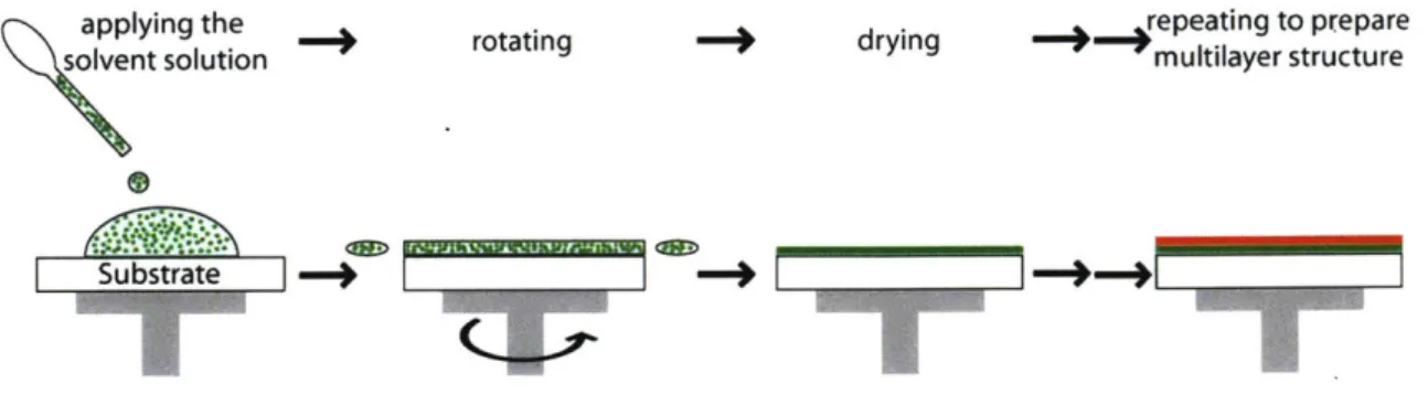
4.2: SPINCOATING
After getting the materials necessary for the project, various solutions with varying concentrations of agar in water were made in order to determine which concentration would work best to spincoat the agar layer. A spincoater is a device that allows for the application of uniform thin films onto flat substrates. An excess amount of the solution of interest is deposited on the substrate (via a pipette for this project) and then rotated at high speeds so that the centrifugal force can spread the
be achieved by using higher rotation speeds on the spincoater as well as
by decreasing the concentration of the solution [12].
applying the rotating -drying repeating to prepare
olvent solution multilayer structure
Figure 7: The spincoating process: apply the solvent solution onto the substrate, then
allow this sample to rapidly rotate, removing any excess solution off the edges. The solution will then dry forming a film on the substrate. Repeat the process to create a multilayer structure.
Source: http://materials.web.psi.ch/Research/ThinFilms/Methods/Images/Spin.jpg
When using a spincoater to create a multilayer structure it is
important that the solvent of the top layer (shown as the red layer in
Figure 7) does not dissolve the layer beneath it (the green layer in Figure
7), and vice-versa or else the structure will be damaged or destroyed. It is
also important that the solvent does not penetrate the titania layer and
swell the agar layer beneath it since this will affect the domain spacing of
the periodic structure. Usually, different solvents are used for each of the
layers to avoid this problem. For this project, however, water was used as
the solvent for both layers (as recommended by Joe Walish) since there
are a very limited amount of edible solvents that can readily dissolve agar
and titania particles. The aforementioned problem was partially avoided
since the agar layer would not dissolve with water once it was in its gel
state (once its temperature reached below 400C). However, water still has the ability to swell the agar gel as described further in Chapter 5.
4.3: PROFILOMETRY
A stylus profilometer allows one to quickly measure the physical thickness of films by dragging a diamond tip on the surface of a sample with very light pressure in order to obtain information about the surface topography (See Figure 8).
x
Styus tip angle.
sampke Ste H. ~
Figure 8: Diagram showing the setup for scanning the surface of a film using a
profilometer. As the stylus moves across the sample it collects information on the topography of the film. The inset shows how the stylus tip can measure the difference in elevation between the film and the sample, which can be then used to determine the film's thickness.
Source: (left) http://probe.olympus-global.com/en/img/PRINCAFM.GIF (right) http://www.wafer-bumping.com/images/graphics/stylustip.jpg
As the tip moves across the surface of a sample it causes a linear variable differential transducer (LVDT) to convert the mechanical signal of
film thickness, though, the samples in this project needed to leave a portion of the substrate uncovered by the film. The agar films were scored using a razorblade (See Figure 9). This didn't work as well for the titania films that were spincoated, however. For the titania films that were sputtered onto the substrate, masking tape was used to cover a small region on the substrate so that once removed, that region of the substrate would not contain any titania.
Figure 9: Photograph of an agar film on a silicon wafer substrate scored using a
razorblade.
This would result in there being a difference in elevation as the stylus moved across the film, which would allow for the calculation of the film thickness by getting the difference in elevation that the profilometer measured. Furthermore, the tip of the stylus used to obtain the profilometry data has a radius of 12.5 microns, with 2.0 mg of force pressing down on the sample as it scanned for lengths ranging between approximately 300 to 1000 microns.
4.4: OPTIMIZING THE CHARACTERISTICS OF THE AGAR FILM
After various experiments that involved going back and forth between the spincoater and profilometer, the optimal concentration, rotation speed, and spincoating time to get a 100 nm layer thickness for agar with a relatively smooth surface were determined to be 2% (agar in water, by mass) spincoated at 4000 revolutions per minute (RPM), for 60 seconds. The graph below is an example of a surface scan obtained using a profilometer. Multiple scans were performed for each sample, covering various regions of the film to check for consistency. Furthermore, this particular scan displays the relatively smooth surface (less than 10 nm difference in elevation throughout) of the 2% agar film spincoated at 4000 RPM (See Figure 10). The drop in the graph corresponds to when the stylus is scanning the surface of the substrate.
2% agar 4K-RPM (scan 1)
120 100 -80 60 -40 II 20 0* --20 "150 00 250 300distance covered by stylus (pm)
Figure 10: Profilometry scan of a 2% agar in water film spincoated at 4000 RPM. The scan length for this run was 300 microns. The thickness of the dry film was determined
The following graph summarizes the trial and error process undergone to determine the rotation speed that would produce films closest to being 100 nm thick for a 3% agar solution, using a spincoater (See Figure 11). Once it was determined that 4000 RPM was the optimal rotation speed, this same speed was used on a 2% agar solution, yielding films with very similar thicknesses. This shows that rotation speed has a greater influence on the thickness of agar films than concentration. The
2% agar film was chosen over the 3% agar film as the optimal
concentration since samples of this concentration displayed smoother surfaces when analyzed with the profilometer.
3% Agar Film Thickness
1000 900 800 700 600 S500 *~400 I- 300 200 100 n -r -# 1st run *2nd run L 3rd run 0 1000 2000 3000 4000 5000 RPM
Figure 11: Variation in film thickness with increasing rotation speed on 3% spincoated
It is important to note that temperature and purity of the agar solutions play a very important role in determining the ability to produce smooth and uniform films of agar. This is because, as mentioned before, agar solidifies into a gel at temperatures between 320C and 400C, keeping the water bound within its gel network and drying out slowly at ambient conditions.
This made it challenging to consistently produce films with the same surface roughness and thickness, despite keeping the concentration and spincoating rate constant. In order to get around this challenge it was necessary to minimize all temperature gradients in the process of spincoating these films and filter the agar solutions with syringe filters that would be able to handle such a viscous liquid (1.5 micron filters were used). This required keeping the agar solution on a hot plate at a
temperature high enough above 400C so that by the time it was
transferred to the substrate (glass or silicon wafer) via a glass pipette and placed on the spincoater properly, it would still remain in the liquid state. If gelling occurred before the sample was spincoated then the sample would not spincoat properly and the sample would exhibit less uniformity throughout.
Measures taken to keep the agar from gelling before being spincoated include keeping the filters, syringes, pipettes, and substrates
temperature changes when the solution would be transferred from one medium to another. After making sure all preparation tools were hot enough, it was necessary to move quickly and minimize the amount of time it took to draw some filtered agar solution with the pipette, release it onto the substrate, carefully center it on the chuck of the spincoater, press the button to create enough suction to keep the sample in place, and finally close the lid of the spincoater while pressing the "start" button. Furthermore, it should be also noted that the step where the agar solution is released from the pipette onto the substrate is very delicate and requires skill to make sure the substrate is uniformly covered. It was also observed that when the substrate would be completely covered by the agar solution, smoother and more uniform samples were produced compared to the ones where only a portion in the center of the substrate was covered.
The following graphs show profilometry scans for agar film samples that were not successfully spincoated (See Figure 12 and Figure 13). These were spincoated at the onset of the trial and error process, before
optimizing the conditions of the spincoating technique and filtering the agar solutions. Hence, the surface roughness of the films represented by the "hills" and "valleys" on the fluctuating white line of the graphs.
Figure 12: Profilometry scan for 0.5% agar film spincoated at 4000 RPM. Scan length was 1020 microns with a speed of 50 microns per second.
Figure 13: Profilometry scan for 1% agar film spincoated at 2000 RPM. Scan length was 1023 microns with a speed of 50 microns per second.
4.5: OPTIMIZING THE CHARACTERISTICS OF THE TITANIA FILM
The same procedure of optimizing the concentration, spincoating rate, and spincoating time was done with titania dispersions but with less success. Food grade titania was obtained from the International Foodcraft Corporation (www.intlfoodcraft.com). Anyhow, like most suppliers of food grade titania, this company did not know much about the characteristics or size of the particles it sells. After multiple phone calls to the company's technical department it was determined that a minimum of 99.5% of the titania particles have to be able to go through a "325 mesh screen" (a filter material with holes smaller than 44 microns) in order to meet company standards [14]. After viewing various concentrations of titania in deionized water dispersions, spincoated between 1000 and 5000 RPM (increasing the rate by 1000 RPM each time) it was determined that this was not the best method to deposit this material. Successful spincoating of the titania layer was a challenge in this project since it produced uneven films with very rough surfaces. This is partly due to the large size of the titania particles and the limited availability of edible solvents. Several profilometry scans for the titania films can be found in the appendix.
4.6: DETERMINING THE SIZE DISTRIBUTION OF TITANIA PARTICLES
Further detailed characterization of the size distribution of the titania particles was done via photon correlation spectroscopy (also known as dynamic light scattering) in order to determine their size distribution and confirm that they would be small enough to make layers that are 50 nm thick. Dynamic light scattering is a technique that uses a laser with a known frequency to direct light at small, moving particles, which then scatter light at a different frequency. This change in the frequency of the light (known as the Doppler shift) is related to the size and velocity of the particles that caused the shift [15]. Since smaller particles have a higher average velocity, they cause a greater shift in the frequency of the light compared to larger particles. By measuring the differences in the frequency and intensity of the scattered light for the different-sized particles present in the sample, the size of the particles can be
determined. The light source used in this experiment was a
monochromatic He-Ne laser with a wavelength of 633 nm. From this technique it was determined that most of the titania particles had diameters that were on the order of about 185.5 nm 20 nm, with some larger particles that had diameters of 463.1 nm 40 nm. These larger diameters may also correspond to clusters of small particles. This data further confirmed that filtering would have to be done in order to get a
may be causing some of the surface roughness on the titania films. It also drew attention to the problem of individual particles stacking on top of each other and creating a rough surface on the film. Most importantly, though, it showed that the titania particles were too large to meet the 50 nm target thickness of the titania layer. Changing the original design of the edible photonic crystal by increasing the target thickness of the titania layer to 200 nm was considered as an option to continue with the spincoating technique, but repeated failure in creating smooth and uniform layers confirmed that a new method was necessary to deposit the titania layers until more studies can be done to overcome the issues with spincoating titania using edible solvents. While there have been successful attempts to spincoat titania nanoparticles into thin films with surface roughness in the order of a few nanometers (as done by J. Yoon et al. to construct a one-dimensional photonic crystal consisting of alternating
layers of titania nanoparticles and polymethylmethacrylate), their
technique made use of butanol to dissolve the titania nanoparticles. Butanol is a polar, organic solvent, but is not safe for human consumption [16].
The graph and accompanying table below give insight to the size distribution of the titania particles (See Figure 14). The vertical axis indicates how many particles (or clusters of particles) of a certain diameter were detected. The taller set of bars on the left corresponds to
the size distribution of single titania particles while the shorter set of bars on the right shows the size distribution of titania particle clusters, or simply much larger particles. G(d) in the table corresponds to the normalized, relative intensity or amount of particles of a certain diameter. The graph and accompanying table show that there are many more single small particles than single large particles or clusters of particles as indicated by a higher G(d) value for diameters in the proximity of 185 nm than for diameters in the proximity of 463 nm (See Figure 12).
100 765 z 25 0.0 Doarmel (nm)
Re1,nt - 100.00 Cum Int. - 68.28 Diam (nm) - 18548
Figure 14: Size distribution of titania particles obtained using the Dynamic Light
Scattering technique. The graph shows the amount of particles of a certain diameter while the accompanying table displays the normalized values that correspond to the data in the graph. Sarrst I T$2 (Coaftred) Oper aOM 11 A EsMed TWO 000230 Mon Ow 214 0 e Rf VW 0173 Skew 2371 d(') O(C g d(nm) 0(d) CQ, 'rvn) O(d) C(d) 1309 0 0 236 0 0 86 4008 0 8 1468 0 0 2476 0 8 420S 5 90 1630 0 0 29 8 0 06 4413 1 94 1605 10 3 2726 0 8 4631 16 98 1685 61 16 2861 0 86 4" 9 7 99 1768 93 42 3W 2 0 86 SM 9 2 100 185 100 63 3150 0 88 6360 0 100 1946 66 83 3306 0 86 5614 0 100 2042 22 86 3469 0 88 581 0 100 2143 0 86 3640 0 86 6182 0 100 2249 0 86 3819 0 86 6487 0 100
4.7: RF-SPUTTERING
Since the spincoating technique was not yielding the smooth titania layers necessary to make the edible photonic crystal, radio frequency (RF) sputtering was used to. deposit these layers. In RF-sputtering, a material of choice (titania for this project) is deposited onto a substrate (such as a silicon wafer) when atoms from the source material, known as the target, detach themselves in vapor form and then condense on the substrate (See Figure 15). The way this technique operates is by first placing the substrate inside a vacuum chamber along with the target and introducing an inert gas, such as Argon, at low pressure [17]. Then, the RF power source generates a plasma, causing the Argon gas to become ionized. These ions then accelerate towards the surface of the target and bombard it, knocking off atoms from the target in the process. These atoms, which are in the vapor form, then condense on the surface of the substrate, generating a film of the source material.
Gas ImpUt Plasma
Tension TVI'" GenerWor
Pumping Sp tted Atoms System
Furthermore, it is better to use an RF power supply which oscillates the electric field instead of a DC power supply for insulating targets, such as titania, in order to avoid charge-build up on the target [18]. Charge-build up on the target can be a serious challenge to successfully sputtering insulating materials since they create a Coulombic barrier that does not allow the Argon ions to interact with the target to detach atoms from it [19]. The parameters used to sputter the titania onto silicon wafer substrates were 300 W of power with a background pressure of 2x10⁻⁶ Torr, Argon pressure of 2 mTorr at a voltage of 800 V. Small silicon wafer substrates were used (2 cm by 2 cm) since there is less accuracy in the film thickness distribution as the size of the substrate increases. This depositing technique produced more uniform titania films, as viewed by the naked eye, compared to the ones made with the spincoater. It was easy to observe a uniform yellow tint throughout the wafer once the titania film had been sputtered onto the wafer, very different from the blue/gray tint of the clean silicon wafer substrate (See Figure 16). It should be noted that after a layer of titania is sputtered, an agar layer is subsequently spincoated on top, producing one pair of alternating layers. When the next layer of titania has to be sputtered on top of the spincoated agar layer, the agar layer will undergo dehydration to varying extents depending on how long the sample is held inside the sputterer under vacuum conditions. This dehydration will cause the agar layer to
decrease in thickness. This process is then repeated until the desired number of total layers is reached.
(a) (b)
Figure 16: a) Photograph of clean silicon wafer substrate before sputtering. b)
Photograph of 30 minute sputtered titania film on silicon substrate displaying yellow tint, confirming successful deposition of the film.
Silicon substrates were sputtered for various times. On one occasion, the sample- was sputtered for 15.5 minutes. In order to determine the growth rate (which can be assumed to be linear with time) of the sputtered titania with the given conditions it was necessary to measure the thickness of the film. Once the growth rate is known, it is then simple to calculate the amount of sputtering time necessary to create a film of a desired thickness. Yet, profilometry did not seem to be able to capture data well for the sputtered samples as shown in the profilometry scan below (See Figure 17). This was probably due to the titania films being too thin for the profilometer to accurately collect data as well as not using the appropriate scan configuration for this specific material (such as
the wrong amount of force applied by the stylus as it scans the sample). Therefore, alternate methods of measuring surface roughness and film thickness had to be considered including ellipsometry and atomic force microscopy.
TiO2 (15.5 min. sample 1, scan 2)
50 40 30' 20' 10 -0' -10' -20 --30 -40 -50 I I I I I I 0 200 400 600 800 1000 1200 1400 distance covered by stylus (pm)
Figure 17: Unsuccessful profilometry scan of titania sputtered for 15.5 minutes.
4.8: ATOMIc FORCE MICROSCoPY
Atomic force microscopy (AFM) was used to characterize the first set
of titania samples, which were sputtered for 15.5 minutes. Once
successfully sputtering this first batch of titania films, it was important to
get the film thickness .in order to figure out the deposition rate for the
surface roughness. AFM is a very high-resolution (fractions of a nanometer) technique that facilitates the study of a material's surface properties at the nanoscale. This technique works by using a flexible cantilever with a nanometer-radius sharp tip (usually made of silicon or silicon nitride) as a probe to scan the surface of a material and measure the size of the deflections the probe undergoes during the process by using a laser spot reflected from the top of the cantilever, and then using this information to generate an image of the surface (See Figure 18) [20]. Furthermore, the deflections that the probe experiences as it scans the surface of a material are caused by forces such as mechanical contact, or if in non-contact mode, Van der Waals interactions along with other chemical forces, magnetic and electrostatic interactions [20]. Some advantages of AFM over the electron microscope include its ability to produce a true three-dimensional surface profile while operating under ambient or even liquid environments (as opposed to a vacuum). Also, sample preparation does not require any special treatment that could destroy the sample or prevent it from being reused [21]. Furthermore, amplitude-modulated tapping mode was used to get the images from the AFM.
,OePhotodiode Las/
Sample Surface Cantilever & Tip
ePZT scanner
Figure 18: Schematic of atomic force microscopy operation mechanism. Source: http://www.uta.edu/ra/cnm/tutorials/afm-tutorial.html
By using AFM, the film thickness of the 15.5-minute sputtered titania sample was determined to be approximately 22 nm. Using a linear model, the deposition rate was calculated to be 1.42 nm per minute. This means that to reach the target thickness of 50 nm for the titania layer, sputtering would need to take place for about 35 minutes and 13 seconds. This makes the manufacturing process of the multilayer stack be really slow. The images below show the surface roughness of the 15.5-minute sputtered titania sample (See Figure 19). Some holes were observed on the film. These are of concern because they can act as channels, allowing the solvent from the third (agar) layer to penetrate the second (titania) layer and potentially swelling, dissolving, or disturbing the first (agar) layer. From a more optimistic standpoint, these pores might actually aid in
the rapid swelling of the agar layers, which is key to the tunability of the structure in practice (discussed in Chapter 5).
-25 nm
Figure 19: AFM images of titania sample sputtered for 15.5 minutes. Left image shows
the boundary between the titania film and silicon wafer substrate (after peeling off the tape). Right image shows the topography of the titania film (notice the darker circular features referred to as pores, indicated by the arrows).
4.9: ELLIPSOMETRY
Unfortunately, there was an unexpected change in the configuration of the RF-sputtering machine (due to efforts to repair it), so it became necessary to repeat the process again of calculating the deposition rate of titania. Hence, a new batch of titania films was sputtered. This time for a
duration of 20 minutes. The films were characterized using ellipsometry. Ellipsometry is a common optical experimental technique that is used to determine the optical constants and thickness of thin films. It is typically used for films whose thickness is on the order of nanometers to a few
microns [22]. Ellipsometry works by measuring changes in light polarization as light reflects or transmits from a material structure [23]. The incident polarized light has elliptical polarization (hence the name of the technique), which combines orthogonal waves of arbitrary amplitude and phase (See Figure 20).
x wave1
wave
Figure 20: Orthogonal waves combine to form elliptical polarization. Source: http://www.jawoollam.com/tutorial_2.html
Light can be separated into orthogonal components. If the electric field of the light is parallel to the plane of incidence it is considered to be p-polarized and if it is perpendicular to the plane of incidence then it is s-polarized [23]. Ellipsometry analyzes how these two components of light change relative to each other with reflection or transmission. In essence, ellipsometry measures the output polarization after a known polarization is reflected or transmitted from the sample (See Figure 21). This change in polarization measured is represented by Equation 2.
where L) is the amplitude ratio and A is the phase difference. These two parameters represent the change in polarization [24].
1. Known input ( ^J.A. Woolam Co. Inc. polarliation E p-plane 3. Measure output polardzation p-ptn E plane of inodence
2. Reflect off sample...
Figure 21: Schematic of ellipsometry operation mechanism showing how incoming
linearly polarized light is reflected off the surface of a sample, and the change in polarization of light is measured to verify the response of the sample.
Source: http://www.jawoollam.com/tutorial_4.html
Furthermore, the complex refractive index, n, is composed of the refractive index, n, which is represented by the real part of Equation 3 and the extinction coefficient, k [22].
{3} n = n +ik
The refractive index as a function of wavelength of the titania film was determined through ellipsometry, with the help of Henry Koh. The approximate value of n for the sputtered titania film is 2.2 over the visible regime. Also, the absorption is quite low (approximately zero) over the same wavelength range (See Figure 22).
Optical Properties of Sputtered Titania (Using Ellipsometry) 31n 1.5 visible rejime 1. - \ k______ ___________ 0 200 300 400 So 600 700 o 9 1000 wavs, (ani)
Figure 22: Graph of the real (n) and imaginary (k) components of the complex
refractive index. The refractive index of the titania film can be approximated to be 2.2 for the visible regime. The extinction coefficient, k, is approximately zero throughout the entire visible regime, meaning that there is very low absorption in the film.
The index of refraction describes the phase velocity of light as it travels in
a material compared to the speed of light in vacuum, c as shown by
Equation 4 [22].
C
{4}
n
As light enters a material with a higher index it slows down its phase
velocity [22]. This, in turn decreases the wavelength of the material since
Air Fim 1 Fim 2
Figure 23: Schematic showing the shortening of the wavelength of light (reduction in phase velocity with constant frequency) as it goes through media with higher index of refraction. Here, ni > n2, and film 1 is an absorbing film, so there is also a reduction in intensity as the light is absorbed during propagation through film 1 before it reaches the transparent second film.
Source: http://www.jawoollam.com/tutorial_2.html
In order to measure the thickness of the film it is necessary to know the optical constants of the material. The thickness is determined by analyzing the constructive and destructive interference between light reflecting from the surface and light that travels through the film, and using the amplitude ratio and phase difference of this interference. Below is a graph of the amplitude ratio for the titania sample. The thickness of
the 20-minute sputtered titania sample was determined to be
approximately 33 nm, yielding a deposition rate of 1.65 nm per minute for the titania. This value is not very different from the deposition rate calculated for the titania sample that was sputtered for 15.5 minutes (1.42 nm per minute) before the machine was altered by the repair. This