HAL Id: cea-00320837
https://hal-cea.archives-ouvertes.fr/cea-00320837
Submitted on 20 Sep 2008
HAL is a multi-disciplinary open access
archive for the deposit and dissemination of
sci-entific research documents, whether they are
pub-lished or not. The documents may come from
teaching and research institutions in France or
abroad, or from public or private research centers.
L’archive ouverte pluridisciplinaire HAL, est
destinée au dépôt et à la diffusion de documents
scientifiques de niveau recherche, publiés ou non,
émanant des établissements d’enseignement et de
recherche français ou étrangers, des laboratoires
publics ou privés.
In-Plane Silicon-On-Nothing Nanometer-Scale Resonant
Suspended Gate MOSFET for In-IC Integration
Perspectives
Cédric Durand, Fabrice Casset, Philippe Renaux, Nicolas Abelé, Bernard
Legrand, Denis Renaud, Eric Ollier, Pascal Ancey, Adrian M. Ionescu, Lionel
Buchaillot
To cite this version:
Cédric Durand, Fabrice Casset, Philippe Renaux, Nicolas Abelé, Bernard Legrand, et al.. In-Plane
Silicon-On-Nothing Nanometer-Scale Resonant Suspended Gate MOSFET for In-IC Integration
Per-spectives. IEEE Electron Device Letters, Institute of Electrical and Electronics Engineers, 2008, 29
(5), pp.494-496. �cea-00320837�
494 IEEE ELECTRON DEVICE LETTERS, VOL. 29, NO. 5, MAY 2008
In-Plane Silicon-On-Nothing Nanometer-Scale
Resonant Suspended Gate MOSFET
for In-IC Integration Perspectives
C. Durand, F. Casset, P. Renaux, N. Abelé, B. Legrand, D. Renaud,
E. Ollier, P. Ancey, A. M. Ionescu, and L. Buchaillot
Abstract—A 14-MHz in-plane nanoelectromechanical resonator
based on a resonant-suspended-gate (RSG) MOSFET principle and integrated in a front-end process is demonstrated. The de-vices are in-plane flexural vibration mode beams (L = 10 µm,
w = 165 nm, and h = 400 nm) with 120-nm gaps. This letter
details the design and process flow fabrication steps. Then, the electrical device characteristics are demonstrated, comprising sta-tic and dynamic studies around the resonant frequency. Devices enable the comparison of a pure capacitive detection with the RSG-MOSFET-based detection on the same component, showing a 4.3-dB-huge peak. Due to its output signal amplification and in-IC integration potentialities, the RSG-MOSFET-based detec-tion is ideal for any type of nanoelectromechanical structure dis-placement detection.
Index Terms—In-IC integration, in-plane resonator,
nanometer-scale resonator, resonant suspended gate (RSG) MOSFET, silicon on nothing (SON).
I. INTRODUCTION
F
OR THE first time, an in-plane nanoelectromechanical (NEM) resonator based on a resonant suspended gate (RSG) MOSFET principle [1], [2] and integrated in a front-end process is demonstrated. Advanced silicon-on-nothing (SON) technology [3] based on industrial 8-in tools is used to fabricate RSG-MOSFETs with high in-IC integration capabilities.This letter reports on the design, fabrication process, mea-surement setup, and experimental results of a 14-MHz NEM resonator and compares a classic capacitive detection [4] with
Manuscript received December 31, 2007; revised February 8, 2008. The review of this letter was arranged by Editor K. De Meyer.
C. Durand is with the STMicroelectronics, 38926 Crolles, France, with the Institut d’Electronique de Microélectronique et de Nanotechnologie (IEMN), CNRS UMR 8520, 59652 Villeneuve d’Ascq, France, and also with the Commissariat à l’ Énergie Atomique (CEA)/Laboratoire d’Électronique et Technologies de l’Information (LETI), Micro and Nanotechnology Innovation Centre (MINATEC), 38054 Grenoble, France (e-mail: [email protected]). F. Casset, P. Renaux, D. Renaud, and E. Ollier are with the Commissariat à l’ Énergie Atomique (CEA)/Laboratoire d’Électronique et Technologies de l’Information (LETI), Micro and Nanotechnology Innovation Centre (MINATEC), 38054 Grenoble, France.
N. Abelé and P. Ancey are with the STMicroelectronics, 38926 Crolles, France.
B. Legrand and L. Buchaillot are with the Institut d’Electronique de Microélectronique et de Nanotechnologie (IEMN), CNRS UMR 8520, 59652 Villeneuve d’Ascq, France.
A. M. Ionescu is with the Electronics Laboratory (LEG), École Polytechnique Fédérale de Lausanne (EPFL), 1015 Lausanne, Switzerland.
Color versions of one or more of the figures in this letter are available online at http://ieeexplore.ieee.org.
Digital Object Identifier 10.1109/LED.2008.919781
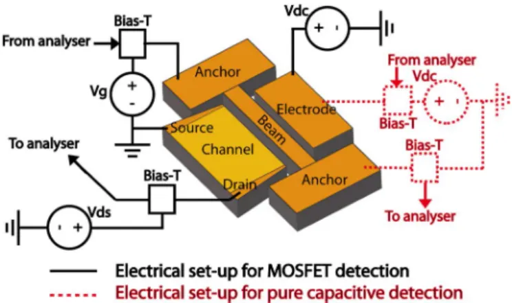
Fig. 1. Principle schematic and electrical characterization setup of the RSG-MOSFET device.
a MOSFET-based detection. Operational dc and vibrating char-acteristics of laterally excited nanogap RSG-MOSFETs are also reported for the first time. The proposed process and fabricated resonators enable the in-IC integration of off-chip modules such as time reference functions with significant cost, size, and consumption reduction [5].
II. DEVICEDESIGN ANDFABRICATION
The lateral MOSFET is composed of a vibrating gate and a channel separated from the mobile gate by an insulator and an air gap (Fig. 1). Drain and source are placed in the same horizontal plane as the gate. The mobile-gate (beam) vibration at resonance frequency modulates the mobile charges of the MOS conductive channel formed along the lateral etched sidewall and, consequently, the drain current. The design and the proposed process enable the integration of both capacitive [4] and amplified detections using the MOSFET intrinsic gain (tailored by the transistor transconductance ids= νgs× gm).
Devices were fabricated by using the SON technology [3] to achieve sub-100-nm gaps and 400-nm-thick single-crystal silicon resonators using only front-end processes [4], [6] and materials, ensuring the in-IC integration capabilities. The fabrication-process flow presented in [4] and [6] is resumed in Fig. 2. It starts with the patterning of active areas through a thermal SiO2 layer. A SiGe sacrificial layer is then grown
by selective epitaxy and followed by a low boron-doped (1016at/cm3) nonselective single-crystal silicon epitaxy.
Phos-phorous dopants are implanted (1019 at/cm3) to define gate,
DURAND et al.: IN-PLANE SON NANOMETER-SCALE RSG-MOSFET FOR IN-IC INTEGRATION PERSPECTIVES 495
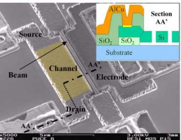
Fig. 2. Perspective SEM picture of a beam (L = 10 µm, w = 165 nm, and
d = 120 nm).
source, and drain. E-beam lithography is used to define gaps and the resonator structure, leading to a 47-nm gap resolution. The 400-nm-thick silicon structural layer is then etched by an anisotropic plasma to define air gaps. After dopant diffusion and activation annealing steps, structures are released by an isotropic plasma etch of the SiGe sacrificial layer. The released structures were protected by a nonconformal SiO2 deposition
to allow metal pad deposition. Fig. 2 shows a picture of a suspended RSG-MOSFET.
III. MEASUREMENTSETUP
RF characterizations are performed by using an Agilent 8753E network analyzer. Fig. 1 shows the two measurement configurations for comparing capacitive and MOSFET detec-tions on the same device.
For a capacitive-detection measurement [4], the transmitted signal through the resonator is measured between the vibrating beam and the electrode of the device. A bias voltage Vdc
is applied on the electrode; the beam and the substrate are grounded to avoid any pull-in effect of the structure.
For a MOSFET-detection measurement, three bias voltages are applied: the electrode Vdc, the gate voltage Vg, and the drain
voltage Vds. Optimal Vgand Vdsvalues for dynamic
character-ization were extracted from the static MOSFET characteristics
Id(Vg) shown in Fig. 3 as well as Id(Vds).
IV. EXPERIMENTALRESULTS
Fig. 3 shows the static electrical Id(Vg) measured
character-istics of the MOSFET transistor. The threshold voltage Vth is
2 V. An OFF-state leakage current of 0.1–1.3 µA depending quasi-linearly on Vdsis observable at Vg= 0 V. It is attributed
to a photolithography misalignment when protecting chan-nel from phosphorous implants. Indeed, chanchan-nel surface was partially implanted on a few nanometer widths, generating a 2.1-MΩ short-circuit resistor in parallel of the transistor, ex-plaining the high leakage current and its quasi-linear depen-dence on Vds. Optimal operating points were defined from
Fig. 3. Static MOS characteristics Id(Vg) and Gm(Vg).
Fig. 4. Capacitive- and MOSFET-detection comparison on the dynamic re-sponse of the NEMS (L = 10 µm, w = 165 nm, and d = 120 nm).
static characteristics: Vg being 4.6 V corresponding to the
maximum of transconductance and Vdsbeing 3 V
correspond-ing to the saturation region, with an OFF-state leakage of 1.4 µA.
Fig. 4 compares the resonant amplitude response between capacitive and MOSFET detections, on the same structure (L = 10 µm, w = 165 nm, and d = 120 nm). The fundamental resonance frequency was measured to be 14.33 and 14.31 MHz with capacitive and MOS detections, respectively. The slight discrepancy between the two measurements is explained by the different bias conditions of actuation between the MOS and capacitive detections. The frequency shift is mainly due to the MOSFET channel surface potential which is set to zero in the case of the capacitive detection. Measurements are in good agreement with mechanical analytical calculations and FEM simulations, giving 14.43 and 14.42 MHz, respectively, being independent of the detection principle. The extracted motional resistance Rm is 736 kΩ, and the C0 capacitance
is 21.5 fF. The MOSFET detection yields a +4.3 dB signal amplification compared with the capacitive detection due to the MOSFET intrinsic gain. This amplitude could be increased first by optimizing the transistor design (channel width/length ratio), hence enabling a higher gm, and second by limiting
the leakages. In this way, the SiGe layer has to be completely etched, and the SiO2insulation layer has to be thicker.
496 IEEE ELECTRON DEVICE LETTERS, VOL. 29, NO. 5, MAY 2008
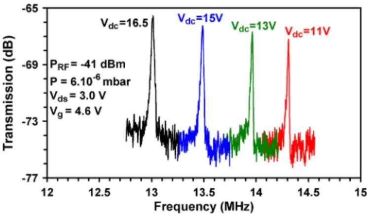
Fig. 5. Influence of Vdc variation on the dynamic response of the NEMS
(L = 10 µm, w = 165 nm, and d = 120 nm) using the MOSFET detection.
Fig. 5 shows the influence of the beam polarization on the output signal using the MOSFET detection. Its amplitude increases with Vdcdue to the larger beam vibration amplitude
caused by the larger electrostatic excitation. The effect is also reinforced by the air-gap reduction induced by the increase in
Vdc. On the other hand, the electrostatic field increases with
Vdcand acts as a negative stiffness, shifting down the resonant
frequency of 10% for a 5.5 V Vdcvariation. The influence of Vds
on the device response was also investigated. Results show an increase in the resonant peak amplitude with Vds, as predicted
on static characteristics for a given Vg of 4.6 V, due to the
increase in gm with Vds. Moreover, a Vds variation from 2.0
to 3.5 V induces a 0.16% decrease in the resonant frequency. This effect is negligible regarding the shift induced by Vdc.
Dependence of resonators’ behavior with environmental con-ditions was studied in [4] on similar devices. Resonant frequen-cies shift down quasi-linearly with temperature (from−50◦C to 100 ◦C), giving a temperature coefficient of frequency of
−32 ppm/◦C. Quality factors were found to be maximum and
constant at low pressure (< 1 Torr), whereas they decrease at
higher pressures, showing that even for nanoscaled beams, air damping remains the major source of dissipation.
V. CONCLUSION
We fabricated and experimentally demonstrated, for the first time, a fully operational in-plane 14-MHz RSG-MOSFET res-onator with intrinsic tunable amplification. The unique large gain, in terms of peak detection amplitude, makes this new device ideal for any type of NEM structure displacement detec-tion. Future works will focus on reliability issues such as fatigue [7], packaging, and in-IC integration for industrial perspectives.
REFERENCES
[1] N. Abelé, R. Fritschi, K. Boucart, F. Casset, P. Ancey, and A. M. Ionescu, “Suspended-gate MOSFET: Bringing new MEMS functionality into solid-state MOS transistor,” in IEDM Tech. Dig., Washington, DC, Dec. 5–7, 2005, pp. 479–481.
[2] D. Grogg, D. Tsamados, N. D. Badila, and A. M. Ionescu, “Integration of MOSFET detection in MEMS resonators for improved output detection,” in Proc. Transducers, Lyon, France, Jun. 10–14, 2007, pp. 1709–1712. [3] S. Monfray, T. Skotnicki, Y. Morand, S. Descombes, M. Paoli, P. Ribot,
A. Talbot, D. Dutartre, F. Leverd, Y. Le Friec, R. Pantel, M. Haond, D. Renaud, M.-E. Nier, C. Vizioz, D. Louis, and N. Buffet, “First 80 nm SON (Silicon-On-Nothing) MOSFETs with perfect morphology and high electrical performance,” in IEDM Tech. Dig, Washington, DC, Dec. 3–5, 2001, pp. 2971–2974.
[4] C. Durand, F. Casset, B. Legrand, M. Faucher, P. Renaux, D. Mercier, D. Renaud, D. Dutartre, E. Ollier, P. Ancey, and L. Buchaillot, “Characteri-zation of In-IC integrable in-plane nanometer scale resonators fabricated by a silicon on nothing advanced CMOS technology,” in Proc. MEMS, Tucson, AZ, Jan. 13–17, 2008, pp. 1016–1019.
[5] C. T.-C. Nguyen, “Vibrating RF MEMS technology fuel for an integrated micromechanical circuit revolution?” in Proc. Transducers, Seoul, Korea, Jun. 5–9, 2005, pp. 243–246.
[6] C. Durand, F. Casset, P. Ancey, F. Judong, A. Talbot, R. Quenouillère, D. Renaud, S. Borel, B. Florin, and L. Buchaillot, “Silicon on noth-ing MEMS electromechanical resonator,” in Proc. DTIP, Stresa, Italy, Apr. 25–27, 2007, pp. 326–331.
[7] A. George, A. Jacques, and M. Legros, “Low-cycle fatigue in silicon: Comparison with fcc metals,” Fatigue Fract. Eng. Mater. Struct., vol. 30, no. 1, pp. 41–56, Jan. 2007.