HAL Id: cea-01791926
https://hal-cea.archives-ouvertes.fr/cea-01791926
Submitted on 18 Feb 2019
HAL is a multi-disciplinary open access archive for the deposit and dissemination of sci-entific research documents, whether they are pub-lished or not. The documents may come from teaching and research institutions in France or abroad, or from public or private research centers.
L’archive ouverte pluridisciplinaire HAL, est destinée au dépôt et à la diffusion de documents scientifiques de niveau recherche, publiés ou non, émanant des établissements d’enseignement et de recherche français ou étrangers, des laboratoires publics ou privés.
Laser-processed three dimensional graphitic electrodes
for diamond radiation detectors
Benoît Caylar, Michal Pomorski, Philippe Bergonzo
To cite this version:
Benoît Caylar, Michal Pomorski, Philippe Bergonzo. Laser-processed three dimensional graphitic electrodes for diamond radiation detectors. Applied Physics Letters, American Institute of Physics, 2013, 103, pp.043504. �10.1063/1.4816328�. �cea-01791926�
1
Laser-processed three dimensional graphitic electrodes for diamond
radiation detectors
Benoît Caylar, Michal Pomorski, Philippe Bergonzo
CEA-LIST, Diamond Sensors Laboratory, Gif-sur-Yvette, F-91191, France
We have used an original approach for diamond detectors where three dimensional buried graphitic electrodes are processed in the bulk of a diamond substrate via laser-induced graphitization. Prototype made of polycrystalline chemical vapor deposition diamond has been fabricated using a nanosecond UV laser. Its charge collection efficiency was evaluated using α-particles emitted by a 241-Americium source. An improved charge collection efficiency was measured proving that laser micro-machining of diamond is a valid option for the future fabrication of three dimensional diamond detectors.
Due to its remarkable physical properties: wide band gap, high charge carrier mobility, and high radiation hardness, diamond exhibits superior interests for the fabrication of radiation detection devices1,2,3. Conventional diamond detectors such as beam position monitors, beam
loss monitors or trackers rely on planar electrodes4,5,6, a configuration where the distance
between collecting electrodes, i.e. the charge carrier drift distance, is defined by the sample thickness. But although diamond devices show extremely high radiation hardness, a degradation of the charge collection efficiency (CCE) could also be observed under prolonged irradiations of the detector, due to radiation damage and related phenomena such as polarization7. An alternative approach has been proposed for silicon by Parker et al8, where the
collecting electrodes are buried within the bulk of the detector and separated by a few dozens of microns. In such a configuration the distance between electrodes, i.e. the charge carrier drift
2
path, is not defined by the sample thickness and can be further reduced. Thus the trapping probability is lowered and higher CCE can be achieved. This geometry is called 3D geometry8,
and a radiation hardness improvement has already been observed in Si from this approach9,10.
Since diamond radiation hardness is far superior to silicon for high energy particles7,11, one can
expect for 3D structured diamond detectors to withstand higher fluences than their silicon analogues and be able to operate after unprecedented radiation levels. Thus future 3D diamond detectors might be interesting candidates for tracking applications in future colliders such as Super Large Hadrons Collider.
Here we demonstrate the possibility to use laser graphitization of diamond to produce 3D electrodes.
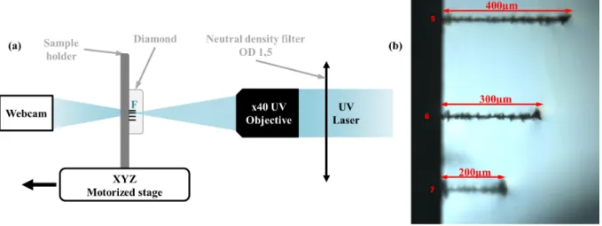
A nanosecond Nitrogen UV laser (MNL 100, Lasertechnik Berlin) operating at λ = 337 nm, was used to induce diamond graphitization12,13. The process consists in focusing a laser
beam beyond the sample thickness and moving it so that the focal point moves backwards through the diamond thickness. By adjusting the stage movement, columns of precise length can be drawn through the sample (Fig. 1(b).). Laser graphitization of diamond with nanosecond pulses (τ=3ns) is a complex phenomenon: during laser irradiation, two processes are competing: conversion of diamond into graphite and graphite sublimation. The graphite generated during the beginning of a laser pulse has a higher absorption than the diamond and a lower thermal diffusion. Thus, the energy contained in the end of the pulse is mainly deposited in the newly formed thin graphite layer, leading to vaporization of this layer at high fluences. In order, to avoid sublimation of graphite a fluence of F=4,72 J.cm-2 was used.
According to the litterature14, this fluence level avoid graphite sublimation. Then the stage was
moved with a 20µm/s velocity, which was high enough to avoid multiple shots on the same graphite part, but also low enough to grow continuous graphitic wires.
3
On Fig.1(b) one can notice large cracks surrounding the electrodes. Indeed when part of the diamond lattice was turned into graphite its density became lower resulting in a volume increase and internal strain formation. Diamond graphitization is a process that takes few picoseconds15. If the laser pulse length is equal or shorter than few picoseconds, it has been
shown15,16,17 that when it ends, a graphite nucleus of minimal dimension is formed without
damage in the crystal lattice due to after-pulse lattice heating. Here nanosecond pulses were used. As a consequence after the formation of the initial graphite nucleus a large amount of energy was still deposited leading to the graphite nucleus overgrowth. It resulted in the creation of highly strained areas where macroscopic cracks occurred because the local strain overcame the diamond tensile strength (2.8 GPa18).
FIG. 1. (Color Online) (a) Laser setup schematic. (b) Optical microscope picture of three graphitic columns with various depths.
Using the setup shown in Fig.1(a), graphitic channels (500µm long, 30µm diameter) were fabricated in a 10x10x0.7mm3 poly-crystalline Chemical Vapor Deposition (pc-CVD)
diamond purchased by Element 6 Ltd. The diamond had two active areas: the first one with graphitic buried electrodes, and the second one with conventional planar electrodes (Fig.2.). The device with planar structure was fabricated as a reference to evaluate the CCE on the same diamond sample and quantify any improvement of the detector performances. The buried
4
structure enables to assess that graphitic columns are electrically active and suitable as electrodes for radiation detector applications.
FIG. 2. (Color online) Electric field simulations [COMSOL Multiphysics] in the hybrid and planar geometries. Electric field color map is in logarithmic scale. (a) Hybrid geometry: an array of 5 by 5 channels (30µm diameter, 500µm depth) with 150µm pitch. The channels are connected all together with an aluminum pad on the top surface. On the back surface, an aluminum pad has been evaporated too. (b) Planar geometry: two aluminum contacts evaporated on the top and back surfaces of the pc-CVD diamond sample.
Dark currents of both structures were measured (Fig. 3) to assess their suitability for radiation detection application. The hybrid device exhibits a leakage current two orders of magnitude above that of the planar device. In fact, this directly results from the shorter distance between graphitic electrodes and the aluminum back contact (200µm) leading to locally enhanced electric fields in the sample. According to electric field simulations achieved at +500V (Fig. 2.), buried electrodes generate a tip termination effect that locally enhances the electric field up to 4V/µm. However, despite these high electric fields, the leakage current remained below 50pA thus making this configuration suitable for radiation detection.
5
FIG. 3. Dark current measurements within both active areas. Planar detector’s characteristic is plotted in filled grey triangle. Hybrid detector’s I(V) curve is plotted in filled black square.
Devices were subsequently tested using α-particles through a collimated 241-Americium source (5,486 MeV α-particles). CCE was measured using a fast charge sensitive amplifier19. The signal was recorded using a Lecroy Wavepro 725Zi digital oscilloscope.
Calibration of the acquisition chain was performed using the same source and a 500µm thick CVD single crystal (Element 6 Ltd.) biased at +500V exhibiting a CCE close to 100% as we already showed in a previous communication20.
FIG. 4. CCE comparison of both devices. α-particles impinging the device from the top (a) or the back (b) sides.
Fig.4 shows spectra of both devices in top and back injection configurations. As no resolved peak can be observed, average efficiencies were calculated as the weighted means of
6
each spectrum. In both configurations, the device with planar electrodes exhibited a CCE of 15% and values up to 50% could be noticed locally most probably correlated with large grains with lower grain boundaries density.
CCE performances of the hybrid device change depending on the side where α-particles were injected. When α-particles were injected from the top side, CCE of only 6% was observed compared to 15% in planar configuration. This behavior was expected from the electric field distribution shown in Fig.2. Two different regimes must be considered in this case : first - electrons are created at the vicinity of the top electrode where the local electric field is very low (0.15V/µm with respect to 0.75V/µm in planar configuration). To contribute to the detection signal, they have to drift in a low gradient electric field along the graphitic columns, during several hundreds of µm before they only enter the high field region for at most 200µm. During the long drift path at low field, the drift distance being low in this kind of pc-CVD material, several electrons will not manage to reach the high electric field region thus nor contribute to the signal, thus explaining the lower detection efficiencies observed when particles are injected from the top side.
On the other hand, when α-particles were injected from the back side, electrons were created in a high electric field region where their drift path is short (only 200µm), and thus more likely to efficiently contribute to the signal. As a result, the hybrid device exhibited an average efficiency of 20% with maximum values reaching 75%. In this configuration, the hybrid device CCE was 1.5 times largerthan the planar one. Data extracted from spectra are consistent with the electric field simulations and show a slight but real improvement in the charge collection properties of the hybrid device compared to planar. However the drift path was reduced by a factor 3.5, so a better improvement of the CCE was expected. Damages and strain created during the electrodes fabrication might be responsible of this by increasing the trapping
7
probability. This constitutes the major drawback of the technique. But it has been shown that using a picosecond21 or femtosecond22 laser can lead to the production of graphitic wires with
minimal surrounding defects.
In conclusion, we reported on the fabrication of 3D graphitic electrodes buried in diamond using laser micro-machining. Our results demonstrate that these electrodes are electrically active and allow charge collection. As a consequence, they appear suitable for future radiation detector applications. However, the electrodes fabrication process still need to be optimized to achieve better CCE. For this, the use of other lasers sources is under investigation. Nevertheless, this work constitutes a major progress toward the fabrication of a 3D diamond detector which could be a significant improvement for radiation hardness issues in high energy physics applications.
ACKNOWLEDGEMENTS
The authors would like to thank Alex ander Oh from The University of Manchester for providing us the diamond sample used in this work.
REFERENCES:
1 P. Bergonzo, D. Tromson, and C. Mer, Semiconductor Science and Technology 18, 105
(2003).
2 P. Bergonzo and R. Jackman, in Semiconductors and Semimetals (2004), p. 197.
3 H. Kagan, Nuclear Instruments and Methods in Physics Research Section A: Accelerators,
Spectrometers, Detectors and Associated Equipment 546, 222 (2005).
4 D. Dobos and H. Pernegger, Nuclear Instruments and Methods in Physics Research Section
A: Accelerators, Spectrometers, Detectors and Associated Equipment 628, 246 (2011).
5 C.J. Ilgner, in 2007 IEEE Nuclear Science Symposium Conference Record (IEEE, 2007),
8
6 R.S. Wallny, Nuclear Instruments and Methods in Physics Research Section A:
Accelerators, Spectrometers, Detectors and Associated Equipment 582, 824 (2007).
7 W. De Boer, J. Bol, A. Furgeri, S. Mueller, C. Sander, E. Berdermann, M. Pomorski, and
M. Huhtinen, Physica Status Solidi A 204, 3004 (2007).
8 S.I. Parker, C. Kenney, and J. Segal, Nuclear Instruments and Methods in Physics Research
Section A Accelerators Spectrometers Detectors and Associated Equipment 395, 328 (1997).
9 A. Kok, G. Anelli, C. Da Via, J. Hasi, P. Jarron, C. Kenney, J. Morse, S. Parker, J. Segal, S.
Watts, and E. Westbrook, Nuclear Instruments and Methods in Physics Research Section A: Accelerators, Spectrometers, Detectors and Associated Equipment 560, 127 (2006).
10 G.-F. Dalla Betta, C. Da Via, M. Povoli, S. Parker, M. Boscardin, G. Darbo, S. Grinstein,
P. Grenier, J. Hasi, C. Kenney, A. Kok, C.-H. Lai, G. Pellegrini, and S. Watts, Journal of Instrumentation 7, 10006 (2012).
11 M. Bruzzi, H.F.-W. Sadrozinski, and A. Seiden, Nuclear Instruments and Methods in
Physics Research Section A: Accelerators, Spectrometers, Detectors and Associated Equipment 579, 754 (2007).
12 T. V Kononenko, V.G. Ralchenko, I.I. Vlasov, S. V Garnov, and V.I. Konov, Diamond and
Related Materials 7, 1623 (1998).
13 T. Okuchi, H. Ohfuji, S. Odake, H. Kagi, S. Nagatomo, M. Sugata, and H. Sumiya,
Applied Physics A 96, 833 (2009).
14 M. Rothschild, C.M. Arnone, and D.J. Ehrlich, Journal of Vaccum Science and
Technologies B 4, 310 (1985).
15 V.N. Strekalov, V.I. Konov, V. V. Kononenko, and S.M. Pimenov, Applied Physics A 76,
603 (2003).
16 C.Z. Wang, K.M. Ho, M.D. Shirk, and P.A. Molian, Physical Review Letters 85, 4092
(2000).
17 V.N. Strekalov, Applied Physics A 80, 1061 (2003).
18 K.K.M. Lee, L.R. Benedetti, A. Mackinnon, D. Hicks, S.J. Moon, P. Loubeyre, F. Occelli,
A. Dewaele, W. Gilbert, and R. Jeanloz, in Shock Compression of Condensed Matter - 2001: 12th APS Topical Conference (2001), pp. 1363–1366.
19 M. Ciobanu, N. Herrmann, K.D. Hildenbrand, T.I. Kang, M. Kis, and a. Schuttauf, 2008
IEEE Nuclear Science Symposium Conference Record 2025 (2008).
20 M. Pomorski, Electronic Properties of Single Crystal CVD Diamond and Its Suitability for
Particle Detection in Hadron Physics Experiments, 2008.
21 M. Shimizu, Y. Shimotsuma, M. Sakakura, T. Yuasa, H. Homma, Y. Minowa, K. Tanaka,
9
22 T.V. Kononenko, V.I. Konov, S.M. Pimenov, N.M. Rossukanyi, a. I. Rukovishnikov, and
![FIG. 2. (Color online) Electric field simulations [COMSOL Multiphysics] in the hybrid and planar geometries](https://thumb-eu.123doks.com/thumbv2/123doknet/13067705.384033/5.892.134.793.188.520/color-online-electric-simulations-comsol-multiphysics-hybrid-geometries.webp)

