Colloid Polym Sci 275:1068-1077 (1997) 9 SteinkopffVerlag 1997
C.J.G. P l u m m e r R. Gensler H.H. K a u s c h
Lattice imaging in melt crystallized
polypropylene thin films
Received: 27 June 1997 Accepted: 15 August 1997
Dr. Christopher J.G. Plummer (12N) Rudolf Gensler " Hans-Henning Kausch I~cole Polytechnique F6d6rale de Lausanne D6partement des Mat6riaux-Laboratoire de Polym6res
MX-D Ecublens
CH-1015 Lausanne/Switzerland
Tel: + 41 21 6932847 Fax: + 41 21 6935868
Abstract Melt crystallized isotactic polypropylene thin films of thickness between 30 and 100 nm have been investigated by high-resolution transmission electron microscopy at room temperature. The c-axis projection of the 2"31 helices and their packing in the lattice were clearly visible in flat-on lamellae of the ~-phase following reconstruction from the components of the image Fourier transform corresponding to the (1 1 0) and (040) lattice planes, and the image power spectra also indicated contributions from (1 3 0) and (0 6 0) relfections, corresponding
to a line resolution of about 0.35 nm. These results are discussed in terms of Bloch wave calculations based on the generally accepted structure for the ~-phase. Attempts to obtain lattice images of the/%phase in isotactic polypropylene and melt crystallized syndiotactic polypropylene under similar operating conditions are also briefly discussed, although these provided relatively little structural information.
Key words T E M H R E M - i s o t a c t i c polypropylene - syndiotactic
polypropylene - image simulation
Introduction
In recent years, there has been considerable use of high- resolution transmission electron microscopy (HREM) to investigate chain packing in semicrystalline polymers [1-5]. Initially, HREM studies were restricted to electron beam resistant polymers, but it has since been demon- strated that the investigation of relatively beam sensitive polymers such as polyethylene [6], poly(tetrafluoroethyl- erie) [7, 8], poly(hydroxybutyrate) [9] and cellulose [10] is also feasible, given suitable precautions against radiation damage. To our knowledge, H R E M studies of polypro- pylene have not so far been reported in the literature, although its crystal architecture has been extensively in- vestigated in the past using scattering techniques [11-21], and there continues to be considerable interest in specific details of the structure of the various polymorphic forms of
both isotactic polypropylene (iPP) and syndiotactic poly- propylene (sPP) [22-28]. Direct lattice imaging of iPP has been shown to be possible using atomic force microscopy (AFM) [29-33], but H R E M may prove to be a useful complementary technique in so far as it provides infor- mation on the internal, possibly defective structure of a sample, whereas A F M is restricted to investigations of the surface morphology.
In what follows we present the results of an HREM investigation of thin melt crystallized polypropylene films, with emphasis on the iPP monoclinic c~-phase, iPP can crystallize in at least two other forms, namely the hexa- gonal //-phase and the triclinic 7-phase [12, 16,28]. Subsequent to rapid cooling or cold drawing, a fourth modification, known as the mesomorphic or smectic phase is also observed, although the details of its crystalline structure are less well known [24, 25]. The ~-modification is the most usual form under normal processing
C.J.G. Plummer et al. 1069 Lattice imaging in polypropylene films
(a)
( b ) u n cq { C 2/c i a a2 P 21/c,'-Z ;_i4 3 / :
-g
u u d dFig. 1 (a) The structure of e - i P P (unit cell viewed along the c-axis):
the two modifications differ in the arrangement of "up" (u) and "down" (d) helices; "L" and "R" indicate left- and right-handed helices; (b) three unit cells of the Ctz-form viewed perpendicular to the chain axis (for clarity the hydrogen atoms are not shown)
conditions. I n d i v i d u a l / 3 - i P P spherulites also occur spor- adically, however, and their formation can be p r o m o t e d by adding/3-nucleants [343.
In each case the i P P chains are packed in the lattice in the form of right- or left-handed 2"31 helices. The helices m a y further be classified as " u p " and " d o w n " helices de- pending on the o r i e n t a t i o n of the methyl side groups with respect to the chain axis. Extensive X-ray studies [13, 14, 18, 19-] have revealed two forms of the monoclinic s-phase, which differ in the configurational arrangement of the helices in the unit cell as shown schematically in Fig. la. The :~l-modification shows r a n d o m packing of " u p " and " d o w n " helices (space group C2/c) and is formed during melt crystallization at high undercoolings [13, 14, 21]. In the m o r e stable ~2-modification, observed at low undercoolings or after annealing at elevated temper- atures [18, 19, 21-1, the helices are packed in alternating
layers of "up" and " d o w n " helices (space g r o u p P21/c) [13, 14]. This is illustrated in Fig. l b where three unit cells of the ~2-modification are shown projected along a*. T h e a r r a n g e m e n t of helices of a given handedness is neverthe- less the same in the two modifications, as s h o w n in Fig. la, and there are only marginal differences in the unit cell parameters (the literature values are generally in the range a = 0.661-0.666nm, b = 2.073-2.098nm, c = 0.6495-0.653 nm a n d / 3 = 98.5 ~ 99.62 ~ [11-15,1).
Experimental
T h e i P P investigated here was an additive free h o m o - p o l y m e r kindly supplied by P C D Polymere, Austria. The weight average molecular weight, Mw, was deter- mined by gel p e r m e a t i o n c h r o m a t o g r a p h y to be a b o u t 300000 g m o l - I and the polydispersity index was 2.97. Thin films were p r e p a r e d by drawing freshly cleaved mica plates from a xylene solution at 140~ under nitrogen. A F M indicated the average thickness of the films to vary between 30 and 50 nm, with local thickness variations of a b o u t 15 20 nm. T o obtain samples with a well defined thermal history, the films were remelted on the mica sub- strate for 30 s at 210 ~ on a hot stage, and subsequently isothermally recrystallized at t e m p e r a t u r e s ranging from 110 to 125~ again u n d e r nitrogen. They were then floated off the substrate o n t o a water bath, m o u n t e d o n c a r b o n coated c o p p e r T E M grids and dried. As an alterna- tive, in order to investigate the feasibility of H R E M invest- igation of free standing films, s o m e w h a t thicker samples ( > 70 nm, as measured by A F M ) were m o u n t e d on coarse- mesh annealed copper grids of the type used by Lauter- wasser and K r a m e r for T E M investigations of crazing [35]. In this case one grid square spans the whole of the T E M sample holder aperture, so that apart from a thin c a r b o n coating to reduce charging, the film is essentially self-supporting. Although s o m e w h a t disadvantageous from the point of view of sample mechanical stability, this m e t h o d m a y evantually p r o v e useful for the o b s e r v a t i o n of deformed samples [36,1. T o reveal a n y edge-on or close to edge-on lamellar structure, certain samples were stained in RuO4-vapour, the stain being p r e p a r e d as described by M o n t e z i n o s et al. [37].
Unless stated otherwise, H R E M was carried out at r o o m t e m p e r a t u r e using the Philips C M 20 (accelerating voltage 200 kV, Cs = 2.0 ram, point resolution 0.28 nm), equipped with a low-dose unit. N o objective a p e r t u r e was used. F o r ~-iPP, the plate magnification in the F O C U S and E X P O S U R E m o d e was generally set to 38 000 • and the exposure times were chosen to be within the total lifetime of the (1 3 0) diffraction spots for the same c o n d e n - ser settings (depending on the film thickness the exposure
1070 C o l l o i d & P o l y m e r Science, Vol. 275, N o . 11 (1997) 9 S t e i n k o p f f Verlag 1997
times at this magnification were at most one third of those given by the a u t o m a t i c exposure meter). Since we worked without an objective aperture and at relatively low magni- fications, it was often difficult to identify the point of Gaussian focus to within more than a b o u t 5 nm (although the presence of small dust particles on the films was helpful in this respect). Once Gaussian focus was found, the image was defocussed by - - 7 0 to - 8 0 nm using the objective lens fine focus control, in order to obtain Scherzer or " e x t e n d e d " Scherzer focus. Again, because of the low mag- nifications used in this study, the a m o u n t of defocus could not be determined a posteori from the experimental im- ages so that the levels of defocus q u o t e d in what follows are subject to an estimated e r r o r of _+ 5 nm. T h e micro- scope was not calibrated for the determination of absolute values of the total end point dose, but the b e a m sensitivity was similar to that of polyethylene. F o r comparison, Revol and M a n l e y [6] have obtained 0.37 nm resolution lattice images of polyethylene single crystals at 1 2 0 k V and at a magnification of 3 6 0 0 0 • with a total dose of
1.8• 10 - 1 1 C t / m -2.
After the first exposure, a second image was recorded in the S E A R C H m o d e at a plate magnification of 11 500 x and at high defocus in o r d e r to situate the initial micro- graph with respect to any coarse features of the sample. T h e images were recorded on K o d a k SO-163 p h o t o - graphic film, developed in full strength K o d a k developer D-19 for 15 min. T h e negatives were then examined with an optical microscope. Regions of interest were digitized using a C C D c a m e r a and transferred to a c o m p u t e r for image analysis. F o r the simulation of H R E M images Bloch wave calculations were carried out using the Elec- tron M i c r o s c o p y Simulation (EMS) software package [38]. Some c o m p l e m e n t a r y multislice simulations were also performed using the Cerius 2 package from Molecular Simulations Inc.
Results and discussion
T h e overall m i c r o s t r u c t u r e of a stained 30 n m thick i P P film, which was melt crystallized at 120 ~ is shown at low magnification in Fig. 2a. In all the samples a two-dimen- sional spherulite-like m o r p h o l o g y was observed, with spherulite radii of the o r d e r of 10/~m. Because o f the limited film thickness and the presence of the substrate during crystallization however, the lamellar o r i e n t a t i o n in these spherulites was expected to be modified with respect to that in thicker spherulitic samples crystallized under equivalent conditions, in which a characteristic cross- hatched a r r a n g e m e n t of lath-like lamellae is observed [39]. When stained, the thinnest films a p p e a r e d relatively featureless at the submicron level at high defocus and
(b)
Tc = 120~
(c)
I rc = !25~
O6O
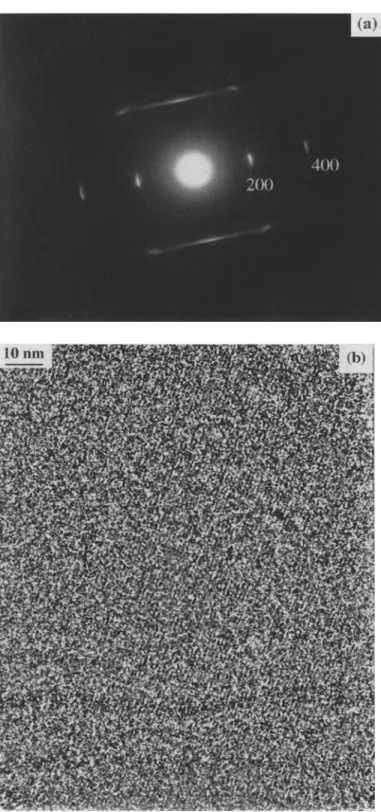
Fig. 2 (a) Microstructure of a thin film isothermally crystallized at 120 ~ and electron diffraction patterns of samples crystallized at (b) 120'~C and (c) 125~
selected area electron diffraction (SAED) suggested a pre- dominantly flat-on a r r a n g e m e n t of the lamellae (Fig. 2b). The coarse microstructure changed little with crystalliza- tion temperature in the range 110-125 ~ although sharp- ening of the S A E D diffraction spots for a g~ven selected area aperture size suggested there to be an increase in spatial coherence with increasing crystallization temper- ature (compare, e.g., Fig. 2b and c).
Figure 3 shows a second image of a sample crystallized at 120~ taken immediately after an initial exposure at high magnification. T h e d a r k circular region resulted from beam damage during focusing, and the light streaks, thought to result from shrinkage during crystallization, lie along the spherutite radii. P a r t of the H R E M lattice image recorded at a b o u t - 7 5 n m defocus is shown in Fig. 4, corresponding to the centre of the region shown in Fig. 3. The image is noisy, reflecting the low exposure times and the granularity of the p h o t o g r a p h i c emulsion, as well as the presence of a m o r p h o u s material in the path of the beam. Nevertheless, two sets of lattice fringes are clearly visible within an irregularly shaped patch whose total area was a b o u t 3 5 x 3 5 n m 2. Figure 5a shows the p o w e r
C.J.G. Plummer et al. 1071 Lattice imaging in polypropylene films
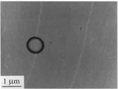
Fig. 3 Typical "second image" taken immediately after initial expo- sure of a film isothermally crystallized at 120 ~ The dark circular region corresponds to the part of the film used for focusing and the HREM image came from the centre of the region shown in the micrograph
Fig. 4 Lattice image in a thin film of iPP isothermally crystallized at 120 ~ obtained at about - 75 nm defocus
spectrum o b t a i n e d form a two dimensional Fast Fourier T r a n s f o r m ( F F T ) of a 256 x 256 pixel image taken from the centre of Fig. 4 (Fig. 5 is in the same orientation as Fig. 4). C o m p a r i s o n of the relative orientation of the fringes vis- ible in Fig. 4 with the positions of the peaks in the power spectrum in Fig. 5a, and the experimental diffraction pat- terns shown in Figs. 2b and 2c, indicates the fringes in Fig. 4 to c o r r e s p o n d to the (040) and (1 10) planes in the ~-iPP unit cell. By tilting the Fig. 4 one can also
(a)
I 1 1 0
L
Fig. 5 (a) FFT power spectrum of part of the lattice image shown in Fig. 4; (b) lattice image reconstructed by Fourier filtering
distinguish a set of (1 i 0) fringes (the a p p r o p r i a t e viewing direction is indicated by the arrow). The c o r r e s p o n d i n g spacings are d110 = 0.626 n m and d0,0 - - 0 . 5 2 n m which are well within the resolution limit of the C M 20, assuming ideal operating conditions.
F o u r i e r filtering was carried out either by m a s k i n g out the noise a n d back transforming, or indirectly by masking the periodic c o m p o n e n t of the F F T , back t r a n s f o r m i n g and subtracting the resulting image from the original im- age. T h e result of filtering is shown in Fig. 5b a n d a further enlargement is given in Fig. 6 along with the p r o j e c t i o n of the unit cell along the [0 0 1] direction. Assuming a lamel- lar thickness of the o r d e r of 10 nm, and correct focussing, it is reasonable to take these images to represent an approxi- m a t i o n to the projected potential of the lattice [-40], in which case the d a r k regions c o r r e s p o n d to the projection of the i P P helices along [ 0 0 1]. T h e periodic a r r a n g e m e n t is clearly consistent with that shown in Fig. I, a l t h o u g h the resolution is insufficient to reveal the pitch of the indi- vidual helices.
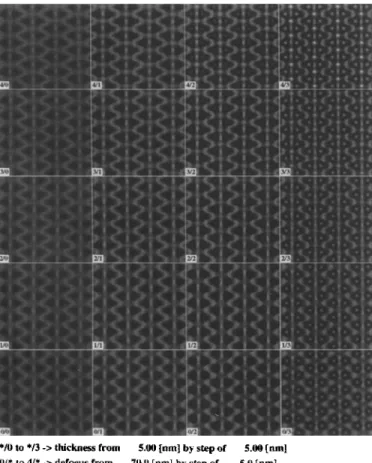
As an aid to m o r e detailed interpretation a n d in o r d e r to identify the o p t i m u m operating conditions for lattice imaging. Bloch wave calculations were carried out using the E M S software package [38] (the helical direction makes no difference to the projected potential along [0 0 1] and so, for convenience, the calculations referred to here are for the e2-modification). T o begin with, we e x a m i n e d the influence of sample thickness (t) and defocus (A f) with the objective a p e r t u r e diameter ( ~ ) set to 7 n m - 1 which corresponds approximately to the resolution limit of the C M 20. Scherzer focus for this microscope ( A f = -- (Cs 2) 1/2) [40] occurs at A f = -- 71 nm, whereas the experimental H R E M images were r e c o r d e d under "extended Scherzer" condi- tions, that is, for somewhat higher values t h a n - 71 n m (typically A f = -- 75 to -- 80 nm). Figure 7 shows simu- lated H R E M images for five A f ( - - 70 to - - 9 0 nm) and four t ( 5 - 2 0 n m ) . F o r t = 5 - 1 0 n m and A f = - - 7 0 to
1072 Colloid & Polymer Science, Vol. 275, No. 11 (1997) 9 SteinkopffVerlag 1997
Fig. 6 Enlargement of Fig. 5b with the c-axis projection of the unit
cell as indicated
r~ E21
of the helices, a n d the p r o j e c t e d p o t e n t i a l a p p r o x i m a t i o n is clearly valid in this r a n g e o f thicknesses, as anticipated above. T h e i m a g e s w h i c h c o r r e s p o n d m o s t closely to the p r o j e c t e d p o t e n t i a l were o b t a i n e d for t = 1 0 n m and A f = - 75 + 5 n m (images 0/1 t o 2/1 in Fig. 7), suggesting the e x p e r i m e n t a l c o n d i t i o n s to be o p t i m a l , a s s u m i n g accu- rate a l i g n m e n t o f the m i c r o s c o p e a n d the sample, a c c u r a t e defocusing, zero objective a s t i g m a t i s m a n d negligible b e a m d a m a g e a n d noise levels. F o r t > 1 5 n m a n d A f < - 75 n m the b e g i n n i n g o f c o n t r a s t reversal can be seen in Fig. 7. C o m p l e t e c o n t r a s t reversal w a s f o u n d to o c c u r at t = 3 0 - 3 5 n m (the c o r r e s p o n d i n g simulated i m a g e s are n o t s h o w n in Fig. 7). H o w e v e r , this is well b e y o n d the e x p e c t e d lamellar t h i c k n e s s of a b o u t 10 n m in i P P samples melt crystallized in the t e m p e r a t u r e range c o n s i d e r e d here ( 1 1 0 - 1 2 5 ~
T y p i c a l e x p e r i m e n t a l lattice i m a g e s of samples crystal- lized at 120~ such as t h a t in Fig. 4, did n o t s h o w r e s o l u t i o n to 0.28 n m , the (1 30) a n d ( 0 6 0 ) reflections being absent, for example. T o m a k e c o m p a r i s o n m e a n i n g - ful, it was therefore n e c e s s a r y to r e d u c e the effective objec- tive a p e r t u r e d i a m e t e r in the s i m u l a t i o n s to between ~Z ~ = 2(d040)- 1 = 2(0.52 n m ) - l = 3.85 n m - 1 a n d ~ = 2(d13o)- 1 = 2(0.4765 n m ) - 1 = 4.2 n m - t. F i g u r e 8 shows a s i m u l a t e d lattice i m a g e for A f - - -- 75 n m a n d t = 10 n m
*/0 to */3 -> thickness from 5.00 [nm] by step of 5.00 [nml
0/* to 4/* -> defocus from 70.0 [nm] by step of 5.0 [ n m ]
Fig. 7 Simulated HREM images of e-iPP in the c-axis projection as a function of defocus (Af) and sample thickness (t)
Fig. 8 SimuIated HREM image of cr in the c-axis projection for Af= -- 75 nm and t = 10 nm; the diameter of the objective aperture was reduced to 23 = 4 nm i to avoid the transmission of the (130) beams
C.J.G. Plummer et al. 1073 Lattice imaging in polypropylene films
where ~3 was set to 4 n m - 1, giving satisfactory agreement with Fig. 6. The absence of(1 3 0) and (0 6 0) reflections was therefore tentatively a t t r i b u t e d to loss of near field order in the lattice owing to b e a m damage.
In H R E M images of samples crystallized at 125 ~ where the degree of local order a n d / o r beam resistance may have increased somewhat, it was nevertheless possible to identify regions such as shown in Fig. 9, for which the image power spectrum did suggest a significant contribu- tion from the (1 3 0) planes. Both the image and the power spectrum have been contrast enhanced for reproduction, but the signal-to-noise ratio in the original image was sufficient to permit F o u r i e r filtering, the results of which are also shown. The agreement with simulations in which the aperture diameter was adjusted to admit the (1 30) beams was less g o o d than in the previous example, al- though the filtered image in Fig. 9c does provide a more accurate representation of the projected potential of the ideal structure. Finally, Fig. 10 shows one of several im- ages taken at a s o m e w h a t lower dose than in Fig. 9, apparently containing contributions from (0 60) ( d o 6 0 ~-
0.347 nm), but in such cases the noise level was too high for simple Fourier filtering to give meaningful results.
It is of course possible to use diffraction data to correct the positions and amplitudes of the Fourier components, assuming the observed phases to be approximately cor- rect, and indeed one can deduce the phases of, and insert reflections which are present in the diffraction pattern, but absent from the image p o w e r spectrum [41]. However, this is t a n t a m o u n t to doing electron crystallography on what is already considered to be a k n o w n structure. It also presup- poses a high degree of periodicity, whereas one of the potential uses of H R E M in polymers is for the observation of lattice defects, for which F o u r i e r filtering is less a p p r o - priate [42, 43]. Indeed we think that defects do contribute substantially to the "noise" in images such as that in Fig. 10, where there is discernible streaking of the (1 1 0) peaks in the p o w e r spectrum. If one looks at the image at an oblique angle the (1 1 0) planes a loss in crystallo- graphic registry is a p p a r e n t on moving across the micro- graph (a clearer example of a defective structure is given below).
F o r T E M of the thicker films m o u n t e d on coarse copper grids, use was m a d e of the Philips E M 430 ST operated at 3 0 0 k V (point resolution 0.2nm, Cs = 1.15 mm). Very similar results to those described above were obtained for the thin films using this microscope under similar operating conditions, and no additional re- flections were detected in the image power spectra. T h e E M 430 ST was nevertheless preferred for films with a nominal thickness of the order of 70 nm owing to the somewhat greater transmission at 300 kV (although A F M suggested the local thickness of the films to vary by a b o u t
Fig. 9 (a) Lattice image of a thin film of iPP isothermally crystallized at 125 ~ (b) FFT power spectrum of (a) showing (13 0) reflections; (c) detail of the corresponding Fourier filtered image; (d) simulated image
Fig. 10 Lattice image of a thin film of iPP isothermally crystallized at 125~ and the corresponding FFT power spectrum showing (06 0) reflections
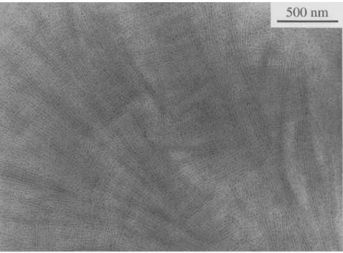
+_ 20 nm, so that individual images did not necessarily c o r r e s p o n d to a total thickness of 70 nm). Figure 11 shows a low magnification, highly defocused image of a stained ca. 70 n m thick film crystallized at l l 0 ~ showing the cross-hatched lamellar structure in part a 2-D spherulite. S A E D nevertheless indicated the presence of a substantial p r o p o r t i o n of flat-on lamellae, which may reflect the influ- ence of the film-substrate interface. Indeed most of the lattice images o b t a i n e d from these samples resembled Fig. 4, showing irregular patches of fringes with [-00 1]
1074 Colloid & Polymer Science, Vol. 275, No. 11 (1997) 9 Steinkopff Verlag 1997
Fig. 11 The cross-hatched lamellar structure of a 70 nm thick iPP film crystallized at 110 ~ and stained with R u O 4
vapour
vertical (dark field m i c r o g r a p h s o b t a i n e d using the (h k 0) reflections also suggested the absence of a regular h a b i t for lamellae in this orientation). N o other crystallographic orientations c o u l d be identified directly f r o m the H R E M m i c r o g r a p h s , a n d no images were o b t a i n e d for lattice planes other t h a n those belonging to the [0 0 1] zone.
M a n y of the images nevertheless showed a distinct m o r p h o l o g y consisting of b a n d s of fringes of between 10 a n d 20 n m in width a n d up to 100 nm or m o r e in length. These were t a k e n to reflect a lath-like lamellar habit. An e x a m p l e is s h o w n in Fig. 12, t a k e n f r o m a sample crystal- lized at l l 0 ~ where one set of(1 1 0) fringes is visible. It was not possible to identify the lamellar o r i e n t a t i o n in this case, but if its l o n g axis is t a k e n to be parallel to a*, the lamellar g r o w t h direction, this lamella m u s t be nearly flat-on. It was therefore inferred that these films c o n t a i n e d lath like lamellae with a wide range of orientations, super- i m p o s e d on a layer of irregularly shaped flat-on lamellae which was in c o n t a c t with the s u b s t r a t e during crystalliza- tion. O f additional interest in Fig. 12 is the a p p a r e n t presence of an a r r a y of crystallographic defects. T h e posi- tion of an a d d i t i o n a l (1 1 0) half plane is indicated b y the arrow, for e x a m p l e (again, tilting the figure helps to see this m o r e clearly). T h e existence of edge dislocations of this type m a y be a n t i c i p a t e d f r o m the fact that the (1 1 0) planes are identical a n d c o r r e s p o n d to a single layer of helices (this is not true of the (0 4 0) planes, for example).
It was also possible to detect spherulites of the hexa- g o n a l / / - p h a s e in these s a m p l e s by S A E D and their p r o p o r - tion could be increased s o m e w h a t by a d d i n g a fl-nucleant
Fig. 12 Part of a lath-like region of(1 1 0) lattice fringes from the film of Fig. 11, apparently containing crystallographic defects (the posi- tion of an extra (1 1 0) half plane is indicated by the arrow)
C.J.G. Plummer et al. 1075 Lattice imaging in polypropylene films
to the solution, although this was less effective for the thinnest films. However, although the /~-lamellae were generally flat-on and their beam sensitivity was compara- ble with that of the a-phase, lattice imaging proved diffi- cult. After several sessions with both the CM 20 the EM 430 ST, using magnifications d o w n to 25 000 • we were unable to detect m o r e than one set of lattice fringes in any given region of the H R E M images, and this was not pursued further.
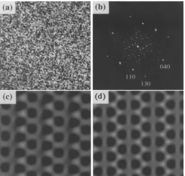
Also disappointing were attempts to obtain lattice im- ages from thin s P P films (the s P P was also supplied by P C D Polymere, Austria). These were melt crystallized on mica at 125 ~ again giving a high p r o p o r t i o n of flat-on lamellae. A typical S A E D pattern is shown in Fig. 13a, showing characteristic streaking of the (0 1 0) and (2 1 0) reflections, which has been identified with an intrinsically defective structure [23, 44]. Briefly, depending on the local handedness of helices being i n c o r p o r a t e d into the lamellae, the chain packing was p r o p o s e d to be either fully isochiral or fully antichiral [23, 44]. In b o t h cases the unit cell is o r t h o r h o m b i c . The nominal parameters for the fully isochiral cell are a = 1.44nm, b = 0 . 5 6 n m , c = 0 . 7 4 whereas for the fully antichiral cell b = 1.12 nm, i.e., the unit cell is doubled along the b-axis [23, 44]. Melt crys- tallized s P P lamellae have been argued to contain a mixture of both modifications, depending on the crystal- lization temperature, and the electron diffraction patterns have been interpreted in terms of various possible defect arrays [23].
Figure 13b shows a typical lattice image of a thin sPP film obtained using the E M 430 ST, showing (2 0 0) lattice fringes with a spacing of 0.72 nm. (0 1 0) and (2 1 0) reflec- tions were absent from most of the image power spectra. This m a y have been due either to beam damage or noise, or a c o m b i n a t i o n of both. T h e intensity associated with diffraction from these planes is likely to spread to along the corresponding layer lines so that the local intensity will diminish with respect to the noise level (in view of the earlier comments concerning/~-iPP, it may be significant that the diffraction patterns f o r / % i P P also showed streak- ing; this is possibly linked to local displacements from the expected positions of helices in a perfectly hexagonal ar- ray, due to "frustrated" packing [28]).
T o gain an idea of what one might hope to observe u n d e r the present operating conditions, a rectangular ar- ray of alternating rows of helices with a row spacing (a/2) of 0.72 nm and a spacing along the rows (b) of 0.56 nm, was constructed using Cerius 2. Starting at r a n d o m positions within the array, half rows were shifted by
b/4
along their lengths to give a mask c o r r e s p o n d i n g to a possible defect structure shown in Fig. 14a [23] (since we are concerned only with the c-axis projection here, no subsequent adjust- ments were made to the handedness of the helices). F o r thisFig. 13 (a) SAED pattern of sPP melt crystallized at 125 ~ (b) a typical lattice image from the same sample, showing (2 0 0) lattice fringes
model structure multislice image calculations were carried o u t for t = 10rim and
A f = -
75 nm, a n d m i c r o s c o p e p a r a m e t e r s c o r r e s p o n d i n g to the E M 430 ST. Figure 14b shows the simulated image, in which the positions of the1076 Colloid & Polymer Science, Vol. 275, No. l l (1997) 9 SteinkopffVerlag 1997
Fig. 14 (a) [00 1] projection of a model defective sPP lattice; (b) multislice simulation from (a) and the corresponding simulated elec- tron diffraction pattern (t ~ 10 nm, A f = -- 75 nm)
defects are clearly visible, along with the simulated elec- t r o n diffraction pattern showing streaking of the (0 1 0) and (2 1 0) peaks, qualitatively consistent with Fig. 13a. When the b a c k g r o u n d noise was included in the simulation by adding the noise c o m p o n e n t of an experimental lattice image (after filtering out the periodic content), to give a m e a n signal to noise ratio of 1:2, we o b t a i n e d images such as shown in Fig. 15a. This illustrates the difficulty inherent in detailed interpretation of H R E M images of s P P taken u n d e r the present conditions. Although the (2 0 0) peaks remain clearly identifiable in the p o w e r spec- t r u m o f this image (Fig. 15b), the intensity of the (010) peaks is reduced, and the associated layer line is substan- tially lost in the noise. Figure !5c shows an experimental image at c o m p a r a b l e magnification, and its p o w e r spec- t r u m (Fig. 15d). Again, the ( 2 0 0 ) peaks are relatively intense, but the (0 1 0) peaks are faint, and the layer lines are a p p a r e n t l y absent. It therefore seems unlikely that one
Fig. 15 (a) Multislice image simulation (t ~ 10 nm and A f = -- 75 nm) using the model of Fig. 14, superposed onto the noise component of an experimental image to give a signal to noise ratio 1 : 2; (b) the FFT power spectrum of image (a); (c) experimental image at comparable magnification; (d) the FFT power spectrum of image (c)
can reconstruct the original, presumably defective lattice from images of this quality by simple F o u r i e r filtering.
Conclusions
Lattice images of the ~-modification of isotactic poly- propylene have been obtained from thin films with spherulitic microstructure using a conventional 200 kV T E M equipped with a low-dose unit, giving a line resolu- tion of up to 0.35 nm. With F o u r i e r fltering, and hence assuming a periodic structure, this should give a c o m p a r a - ble effective point resolution as long as the intensities of Bragg peaks in the image power spectrum are higher than the total noise intensity within the masks. However, the noise level becomes m o r e critical for defect structures, in which the Bragg peaks m a y be b o t h diminished in inten- sity and smeared out over a wider range of spatial frequen- cies. O u r attempts to obtain H R E M images of melt crystallized s P P are a case in point. Even assuming the microscope p a r a m e t e r s to be optimized (which the results for e - i P P a p p e a r to confirm) and leaving aside extrinsic factors such as sample misalignment and beam damage, the effective resolution is severely limited by b a c k g r o u n d noise imposed by the need to underexpose the negatives, the granularity of the film and contributions to the image
C.J.G. Plummer et al. 1077 Lattice imaging in polypropylene films
from a m o r p h o u s m a t e r i a l ( i n c l u d i n g the c a r b o n s u b s t r a t e ) a n d l a m e l l a e w h i c h are n o t in a Bragg o r i e n t a t i o n .
It m i g h t be of i n t e r e s t to m o d i f y the s a m p l e p r e p a r a - t i o n c o n d i t i o n s in o r d e r to r e d u c e the s u b s t r a t e a n d s a m p l e t h i c k n e s s , a n d to i n c r e a s e the local o r d e r (e.g., b y c r y s t a l l i z i n g at h i g h e r t e m p e r a t u r e s ) . H o w e v e r , well o r d e r e d s P P s a m p l e s h a v e a l r e a d y b e e n e x t e n s i v e l y c h a r - acterized b y A F M o f l a m e l l a e c r y s t a l l i z e d e p i t a x i a l l y f r o m the melt o n t o s o l u b l e s u b s t r a t e s [32]. I n d e e d , w h e r e a s T E M is r e s t r i c t e d to o b s e r v a t i o n of z o n e s c o n t a i n i n g s t r o n g l y d i f f r a c t i n g p l a n e s , A F M c a n give access to a m u c h wider r a n g e of s t r u c t u r a l d e t a i l in such samples. A F M
i m a g i n g of defect s t r u c t u r e s i n the [ 0 0 1] p r o j e c t i o n of d i s o r d e r e d m e l t c r y s t a l l i z e d s P P l a m e l l a e n e v e r t h e l e s s re- m a i n s s o m e w h a t o f a c h a l l e n g e e x p e r i m e n t a l l y , n o t l e a s t b e c a u s e of t h e p o t e n t i a l l y r o u g h fold surfaces o f a s - c r y s t a l - lized s a m p l e s .
Acknowledgments The TEM work was carried out at the Electron Microscopy Center (CIME) of the EPF Lausanne, and we are in- debted to Prof. P. Stadelmann and Dr. C. Beeli (CIME) for helpful comments concerning image simulation. We also would like to thank Dr. E. Kramer, Ciba-Geigy, Basic, Switzerland, and Dr. W. Neil31, PCD Polymere, Linz, Austria, for helpful discussions and samples, and Ciba-Geigy, Switzerland for financial support (RG).
References
1. Uemura A, Tsuji M, Kawaguchi A, Katayama K (1988) J Mater Sci 23:1506-1509
2. Voigt-Martin IG, Garbella RW,
Schumacher M (1992) Macromolecules 25:961 971
3. Fryer JR, Dorset DL (1991) Electron Crystallography of Organic Molecules. Kluwer Academic Publishers, Dor- drecht
4. Tsuji M, Kohjiya S (1995) Prog Polym Sci 20:259-308
5. Martin DC, Thomas EL (1995) Polymer 36:1743 1759
6. Revol J-F, John Manley RS (1986) J Mater Sci Lett 5:249 251
7. Chanzy HD, Folda T, Smith P, Gardner K, Revol J-F (1986) J Mater Sci Lett 5:1045 1047
8. Plummer CJG, Kausch H-H (1996) Polymer Bulletin 37:393-397
9. Revol J-F, Chanzy HD, Deslandes Y,
Marchessault RH (1989) Polymer
30:1973 1976
10. Revol JF (1985) J Mater Sci Lett 4: 1347 1349
11. Natta G, Corradini P (1960) Del Nuovo Cimento Suppl 15:40 51
12. Turner Jones A, Aizlewood AM, Beckett DR (1964) Makromol Chem 75:134-158 13. Mencik Z (1972) J Macromol Sci-Phys
B 6:101 115
14. Hikosaka M, Seto T (1973) Polymer J 5:111-127
15. Immirizi A (1980) Acta Crystallogr B 36:2378 2385
16. Corradini P, Petraccone V, Pirozzi B (1983) Eur Polym J 19:299-304 17. Lovinger AJ (1983) J Polym Sci Polym
Phys 21:97 110
18. Guerra G, Petraconne V, Corradini P, De Rosa R, Napolitano R, Pirozzi B, Giunchi G (1984) J Polym Sci Polym Phys 22:1029 1039
19. De Rosa C, Napolitano RVP, Pirozzi B (1984) Eur Polym J 20:937 941 20. Lotz B, Wittmann JC (1986) J Polym Sci
- Polym Phys 24:1541 1558
21. Napolitano R, Pirozzi B, Varriale V (1990) J Polym Sci - Polym Phys 28: 139 147
22. Ferro DR, Briickner S, Meille SV, Ragazzi M (1992) Macromolecules 25: 5231 5235
23. Lovinger AJ, Lotz B, Davis DD, Padden Jr FJ (1993) Macromolecules 26: 3494~3503
24. Yan RJ, Li W, Li G, Jiang C (1983) J Macromol Sci - Phys B 32:15 25. Caldas V, Brown GR, Nohr RS, Mac-
Donald JG, Raboin LE (1994) Polymer 35:899-907
26. Meille SV, Ferro DR, Bruckner S, Lovinger AJ, Padden FJ (1994) Macro- molecules 27:2615 2622
27. Bu Z et al (1996) Macromolecules 29: 6575 6581
28. Lotz B, Wittmann JC, Lovinger AJ (1996) Polymer 37:4979 4992
29. Lotz B, Wittmann JC, Stocker W, Magonov SN, Cantow HJ (1991) Polym Bull 26:209-214
30. Snetivy D, Guillet JE, Vansco GJ (1993) Polymer 34:429 431
31. Stocker W, Magonov SN, Cantow H J, Wittmann JC, Lotz B (1993) Macro- molecules 26:5915 5923
32. Stocker W, Schumacher M, Graft S, Lang J, Wittmann JC, Lovinger A J, Lotz B ( 1 9 9 4 ) Macromolecules 27:6948 6955
33. Tsukruk V, Reneker DH (1995) Macro- molecules 28:1370-1376
34. Huang MR, Li XG, Fang BR (1995) J Appl Polym Sci 56:1323
35. Lauterwasser BD, Kramer EJ (1979) Phil Mag 39A:469-495
36. Plummer CJG, Kausch H-H (1997) Macromol Chem Phys 198:485-493 37. Montezinos D, Wells BG, Burns JL
(1985) J Polym Sci Polym Lett 23:421 38. Stadelmann PA (1987) Ultramicroscopy
21:131 146
39. Norton DR, Keller A (1985) Polymer 26:704-716
40. Reimer L (1993) Transmission Electron Microscopy. Springer, Berlin
41. Dorset DL (1994) In: Spells SJ (ed) Char- acterization of Solid Polymers - New Techniques and Developments. Chap- man & Hall, London, pp 1 16
42. Prad6re P, Revol JF, John Manley RS (1988) Ultramicroscopy 25:69
43. Martin DC, Thomas EL (1987) MRS Bull XII:27-37
44. Lotz B, Lovinger A, Cais RE (1988) Macromolecules 21:2375 2382