Publisher’s version / Version de l'éditeur:
ACS Applied Materials & Interfaces, 2016-09-23
READ THESE TERMS AND CONDITIONS CAREFULLY BEFORE USING THIS WEBSITE.
https://nrc-publications.canada.ca/eng/copyright
Vous avez des questions? Nous pouvons vous aider. Pour communiquer directement avec un auteur, consultez la
première page de la revue dans laquelle son article a été publié afin de trouver ses coordonnées. Si vous n’arrivez pas à les repérer, communiquez avec nous à PublicationsArchive-ArchivesPublications@nrc-cnrc.gc.ca.
Questions? Contact the NRC Publications Archive team at
PublicationsArchive-ArchivesPublications@nrc-cnrc.gc.ca. If you wish to email the authors directly, please see the first page of the publication for their contact information.
Archives des publications du CNRC
This publication could be one of several versions: author’s original, accepted manuscript or the publisher’s version. / La version de cette publication peut être l’une des suivantes : la version prépublication de l’auteur, la version acceptée du manuscrit ou la version de l’éditeur.
For the publisher’s version, please access the DOI link below./ Pour consulter la version de l’éditeur, utilisez le lien DOI ci-dessous.
https://doi.org/10.1021/acsami.6b06838
Access and use of this website and the material on it are subject to the Terms and Conditions set forth at
Fully printed and encapsulated SWCNT-based thin film transistors via a
combination of R2R gravure and inkjet printing
Homenick, Christa M.; James, Robert; Lopinski, Gregory P.; Dunford, Jeffrey;
Sun, Junfeng; Park, Hyejin; Jung, Younsu; Cho, Gyoujin; Malenfant, Patrick
R. L.
https://publications-cnrc.canada.ca/fra/droits
L’accès à ce site Web et l’utilisation de son contenu sont assujettis aux conditions présentées dans le site LISEZ CES CONDITIONS ATTENTIVEMENT AVANT D’UTILISER CE SITE WEB.
NRC Publications Record / Notice d'Archives des publications de CNRC:
https://nrc-publications.canada.ca/eng/view/object/?id=5c9e5f2f-e987-427a-a147-3f9bc515eded https://publications-cnrc.canada.ca/fra/voir/objet/?id=5c9e5f2f-e987-427a-a147-3f9bc515eded
Fully Printed and Encapsulated SWCNT-Based Thin Film Transistors
via a Combination of R2R Gravure and Inkjet Printing
Christa M. Homenick,
*
,†Robert James,
‡Gregory P. Lopinski,
†Jeffrey Dunford,
§Junfeng Sun,
∥Hyejin Park,
∥Younsu Jung,
∥Gyoujin Cho,
*
,∥and Patrick R. L. Malenfant
*
,§†
National Research Council Canada, 100 Sussex Drive, Ottawa, Ontario K1A 0R6, Canada ‡
RF Technologies Ottawa, Communications Research Centre Canada, Nepean, Ontario K2H 8S2, Canada §
National Research Council Canada M-50, 1200 Montreal Road, Ottawa, Ontario K1A 0R6, Canada
∥Department of Printed Electronics Engineering, Sunchon National University Suncheon, Jeonnam 540-742, Republic of Korea
*
S Supporting InformationABSTRACT: Fully printed thin film transistors (TFT) based on poly(9,9-di-n-dodecylfluorene) (PFDD) wrapped semi-conducting single walled carbon nanotube (SWCNT) channels are fabricated by a practical route that combines roll-to-roll (R2R) gravure and ink jet printing. SWCNT network density is easily controlled via ink formulation (concentration and polymer:CNT ratio) and jetting conditions (droplet size, drop spacing, and number of printed layers). Optimum inkjet printing conditions are established on Si/SiO2in which an ink consisting of 6:1 PFDD:SWCNT ratio with 50 mg L−1 SWCNT concentration printed at a drop spacing of 20 μm results in TFTs with mobilities of ∼25 cm2V−1s−1and on-/off-current ratios > 105. These conditions yield excellent network uniformity and are used in a fully additive process to fabricate
fully printed TFTs on PET substrates with mobility values > 5 cm2V−1s−1(R2R printed gate electrode and dielectric; inkjet printed channel and source/drain electrodes). An inkjet printed encapsulation layer completes the TFT process (fabricated in bottom gate, top contact TFT configuration) and provides mobilities > 1 cm2V−1s−1with good operational stability, based on the performance of an inverter circuit. An array of 20 TFTs shows that most have less than 10% variability in terms of threshold voltage, transconductance, on-current, and subthreshold swing.
KEYWORDS: fully printed, thin film transistor, enriched semiconducting carbon nanotube ink, SWCNT ink formulation, roll-to-roll
1. INTRODUCTION
Printed electronics has garnered significant attention in recent years as a result of its potential to enable low-cost, high-throughput manufacturing of flexible electronics on plastic substrates for applications such as flexible displays, logic circuits, sensors, oscillators, and radio frequency identification (RFID) tags.1−3 Realization of these applications requires selection of materials and optimization of printing processes for the fabrication of fully printed thin film transistors (TFTs) with good stability and uniformity of threshold voltage (Vth).4 Careful selection of semiconducting material such that it provides robust performance via printing will therefore be a key step to provide well-behaved fully printed TFTs. Among many printable semiconducting inks, semiconducting single walled carbon nanotubes (SWCNTs) have attracted the attention of the printed electronics community as a promising printable channel material due to their robustness, flexibility, and high intrinsic carrier mobility.5−8
Initial attempts at printing SWCNT channels utilized solutions containing a mixture of semiconducting and metallic
SWCNTs.9−11The presence of metallic SWCNTs in networks
formed from these solutions resulted in conducting paths that could not be turned off with gate voltage, limiting the on/off ratio of TFTs formed from these inks. Okimoto et al. circumvented this limitation by controlling the network density below the percolation threshold for the metallic SWCNTs;11 however, the sparse networks required to maintain high on/off ratios (>103) limited the driving currents in these devices. Availability of highly enriched semiconducting SWCNT dispersions has dramatically improved driving currents while maintaining high on/off ratios of TFTs based on solution processed SWCNT networks. For example, the separation of metallic and semiconducting SWCNTs via density gradient ultracentrifugation12,13 facilitated the demonstration of fully
printed SWCNT TFTs with on/off ratios ranging from 104to 107, mobilities of 10−30 cm2V−1s−1, and on-currents sufficient
Received: June 8, 2016 Accepted: September 23, 2016
www.acsami.org
© XXXX American Chemical Society A DOI:10.1021/acsami.6b06838
to drive an OLED pixel.14 Further advances in SWCNT separation have made possible the production of SWCNT dispersions with greater than 99% semiconducting purity via a variety of methods.15−23 Recently, a polymer separation
method based on poly(9,9-di-n-dodecylfluorene) (PFDD) was demonstrated to be an effective and efficient method for producing samples of >99.9% semiconducting dispersions.19,23 Many impressive demonstrations implementing enriched semiconducting SWCNT materials as a channel in transistor and circuit applications have used vacuum filtration and transfer24−26 or solution casting20,27−32 to deposit the
SWCNT network. These methods, however, require additional steps such as photolithography or ozone plasma etching to pattern the channel material. Alternatively, direct printing of the SWCNT channel has been demonstrated by a variety of techniques including inkjet14,33−36and aerosol.21,37−40Device
fabrication has been completed by vacuum deposition of gate dielectric and/or source/drain electrodes in some cases and fully printed TFT material layers in others.14,34,35Furthermore, examples of fully printed SWCNT-based TFTs employing roll-to-roll (R2R) printing are rare4,41,42 and have yet to be
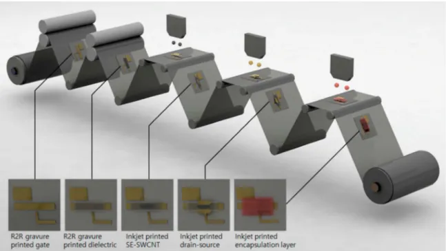
demonstrated with semiconducting-enriched SWCNT with a printed encapsulation layer to provide environmental stability. Herein, the efficacy of a hybrid printing system comprising R2R gravure and inkjet is examined in order to practically produce SWCNT-based fully printed TFTs with encapsulation to avoid environmental sensitivity of the SWCNT channel. The intrinsic difficulty associated with formulating enriched SWCNT semiconductor for gravure printing (high viscosity > 100 cP) led us to select inkjet printing that requires less than 10 cP. As a result, the relationship between jetting conditions of PFDD/SWCNT-based inks for inkjet printing of TFT channels on Si/SiO2test chips and the resulting electrical characteristics of printed TFTs was first investigated. Building on this knowledge, an all additive manufacturing approach incorporat-ing hybrid R2R gravure and inkjet printincorporat-ing processes was studied to fabricate fully printed TFTs. This hybrid process incorporates R2R gravure to print the gate electrodes and dielectric and then an inkjet process to print the PFDD/ SWCNT channel, source/drain electrodes, and an encapsula-tion layer. A potential all additive manufacturing method is shown inScheme 1, in which R2R gravure and inkjet processes Scheme 1. Schematic of an Integrated R2R Gravure/Inkjet Printing System for Fully Printed SWCNT TFTs on Plastic Foila
aIn the current work described herein, only the gate and dielectric were R2R printed, whereas the channel, S/D electrodes, and encapsulant were
inkjet printed in batch mode.
Figure 1.Time lapse images of the ink drop versus the distance the drop has fallen from the nozzle during optimized jetting of the SWCNT ink at 5 m s−1(50 mg L−1; PFDD:SWCNT ratio, 6:1).
DOI:10.1021/acsami.6b06838
ACS Appl. Mater. Interfaces XXXX, XXX, XXX−XXX
are combined within one fully integrated printing system to fabricate fully printed thin film transistors complete with encapsulation to provide device stability.
2. RESULTS AND DISCUSSION
Using PFDD/SWCNT powder, a series of SWCNT inks were prepared in toluene with a SWCNT concentration of 10, 50, 93, or 110 mg L−1and a polymer to nanotube ratio of 1:1, 3:1, 6:1, or 8:1. Starting with the lowest SWCNT concentration ink (10 mg L−1, 3:1), the printing waveform and cartridge settings were modified to produce stable jetting of 10 pL drops (Figure 1), with each drop of ink traveling at 5 m s−1. As the concentration increased, clogging of the nozzles became more frequent, resulting in drops being ejected from the print head at spurious angles, limiting pattern fidelity. At SWCNT concentrations > 100 mg L−1 jetting performance was too poor to produce an acceptable transistor channel; therefore, the printing studies were limited to inks that could be reliably jetted.
Similar to the findings of Cui and co-workers,39 surface
modification using oxygen plasma to alter the wetting of SWNT droplets on the SiO2was found to be critical to achieve good print resolution and SWCNT adhesion. Plasma treatment was found to consistently produce a uniform surface, which led to good wetting of the SWCNT ink (Figure 2).
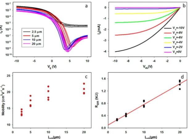
2.1. Effect of Layering. Initially the lowest concentration SWCNT ink (10 mg L−1, 3:1) was inkjet printed onto silicon test chips using 20 μm drop spacing. While functioning transistors were obtained, the on-current densities and mobilities obtained were considerably lower than those observed for soaking using similar PFDD/SWCNT solutions.19 Transistors with channel lengths of 20 μm resulted in an average hole mobility of less than 10 cm2V−1s−1with on/off ratios of ∼106. Adding additional layers was found to increase the mobility and on-currents without decreasing the on/off ratio (Supporting InformationFigure S1). This layering process results in a dense uniform network spanning the source and drain (Figure S2). Typical device performance from a test chip with four layers of the low-concentration SWCNT ink was measured (Figure 3). Transfer curves show all 16 devices on the chip are functional (Figure 3a). Devices with 2.5 μm channel lengths exhibit a limited on/off ratio of ∼103likely due to metallic percolating paths between source and drain. Although the SWCNTs used have very low content of metallic tubes, the high density of tubes in these networks, short channel length, and large device width (2 mm) all lead to an increased probability of a metallic path between the source and drain. Based on a percolation model, an estimated network density of 100 tubes/μm2and a nanotube length of 1.2 μm, a single metallic path is probable for a metallic tube fraction of
0.02%, consistent with previous estimates of SWCNT purity in these samples.43For longer channel lengths, the TFTs exhibit on/off ratios of ∼106. These devices also show the appearance of a weak n-channel for positive gate voltages. This weak ambipolar behavior with a dominant p-channel is characteristic of SWCNT TFTs measured in ambient on hydrophilic substrates such as SiO2due to the effect of the water−oxygen redox couple.44The output characteristics for a 20 μm device indicate current densities of 2 mA mm−1 are achieved in saturation (Figure 3b).
Channel length dependence of the mobility and on-state resistance of the inkjet printed SWCNT TFTs were also evaluated (Figure 3c,d). Lower effective mobilities were obtained for the shorter channel lengths with the mobility increasing to >20 cm2V−1s−1for 20 μm channels. When the on-state resistance of the channel is plotted as a function of the channel length (Figure 3d), the slope of the linear fit to this data set yields the channel resistance per micrometer (67 Ω μm−1) while the y-intercept corresponds to 2R
c, where Rcis the contact resistance (48 Ω).45Normalizing the resistance to the width of the contacts yields 96 kΩ·μm, which is consistent with literature results for SWCNT network TFTs.28,46This analysis indicates that the contact resistance plays a significant role in limiting the performance for shorter channel devices L < 10 μm while being less important for longer channels; thus, 20 μm channel length devices were used going forward. These results indicate that it is possible to improve TFT performance by adding additional layers of SWCNT ink onto the substrate; however, eight consecutive prints of SWCNT ink (10 mg L−1) deposited enough solvent on the SiO2 surface to exceed the surface tension of the pattern edge. As a result, pattern fidelity could only be marginally maintained (Figure S3) and printing of additional layers (beyond eight) was not beneficial because pattern resolution was lost.
2.2. Effect of Drop Spacing and Concentration. While the layering results showed that it is possible to obtain good performance by using several passes with a low SWCNT concentration ink, printing of multiple layers is not the preferred route if one intends to integrate with a R2R gravure system and may lead to resolution and registration issues. As a result, printing with higher concentration inks (50 and 93 mg L−1; SWCNT:PFDD ratio of 1:1) was investigated to determine if good TFT performance could be obtained in a single pass, further improving the efficiency of the process and making it more compatible with a continuous process such as roll-to-roll printing. Furthermore, as smaller spacing between successive drops results in more material deposited in a given area, varying drop spacing is a convenient way to explore the effects of ink volume per unit area on print quality and TFT performance using a single pass. TFT performance was measured as a function of drop spacing using two high-concentration inks (Figure 4). Each of the points represents an average over the four 20 μm channel length devices on a single chip. Devices printed with the 93 mg L−1ink at a drop spacing ≤ 20 μm exhibit mobilities of ∼30 cm2V−1s−1, and on-state current densities greater than 0.75 mA mm−1(at V
ds= −1 V), indicating excellent TFT performance can be obtained in a single pass. Smaller drop spacing (larger SWCNT volumes) resulted in the highest on-currents but also larger off-currents, leading to on/off ratios < 103. The limited on/off ratios at smaller drop spacing likely reflects the contribution of the very low fraction of residual metallic tubes (0.02%) in these high-density networks (vide supra). For drop spacings above 20 μm
Figure 2. Images of inkjet printed SWCNT patterns (10 mg L−1;
PFDD:SWCNT ratio, 3:1; single layer with a 20 μm drop spacing) obtained on (a) untreated SiO2and (b) oxygen plasma treated.
DOI:10.1021/acsami.6b06838
ACS Appl. Mater. Interfaces XXXX, XXX, XXX−XXX
the off-current decreased below 10−7A, leading to on/off ratios > 104. The mobility also decreased at higher drop spacing where the amount of SWCNTs deposited on the surface was reduced. The 20 μm drop spacing is seen to be optimal to maximize mobility and on/off ratio for the 93 mg L−1 ink (Figure 4).
Similar behavior was observed using the 50 mg L−1ink (only drop spacing less than 25 μm was explored for this ink). Overall the differences between the two concentrations are small, despite almost doubling the concentration of SWCNTs within the ink and hence the material deposited. SEM images of these devices revealed networks whose density was too high (>100
tubes μm−2) to be estimated by counting. Raman microscopy was used to obtain information on relative network densities on these surfaces (Figure S4). The amount of SWCNTs on the surface after rinsing increased with the amount of material deposited, saturating at smaller drop spacing (<15 μm for the 93 mg L−1 ink). Saturation for large amounts of material deposited indicates that the SWCNT network density after rinsing is self-limiting. More significantly, comparison of the Raman and electrical data indicates that the mobility and on-currents reach a plateau before the amount of SWCNTs on the surface saturates. For example, devices printed at a 20 μm drop spacing with the two different ink concentrations exhibit rather
Figure 3.(a) Transfer curves (Vds= −1 V) for TFTs of different gate lengths (W = 2 mm) with inkjet printed SWCNT channels (10 mg L−1; 3:1
PFDD:SWCNT ratio; four layers at 20 μm drop spacing) on Si test chips (90 nm SiO2gate dielectric and evaporated Ti/Au bottom contacts). (b)
Output characteristics for a TFT with L = 20 μm. (c) Mobility as a function of channel length extracted from transfer curves in a. (d) On-state resistance as a function of channel length. The slope of the linear fit to these data represents the channel resistance per micrometer, and the y-intercept corresponds to 2Rc, where Rcis the contact resistance.
Figure 4.Mobility (a) as well as on- and off-currents (b) for TFTs with 20 μm × 2000 μm channels printed with two different concentration SWCNT inks (SWCNT:PFDD ratio of 1:1) for various drop spacings on Si test chips (90 nm SiO2gate dielectric and evaporated Ti/Au bottom
contacts).
DOI:10.1021/acsami.6b06838
ACS Appl. Mater. Interfaces XXXX, XXX, XXX−XXX
similar mobility and on-currents even though the SWCNT network density is roughly twice as high for the higher concentration ink. This result implies that in this range the mobility and on-currents reach a saturation point, and additional tubes do not contribute to the electrical transport. Raman was also used to determine that 35−55% of the deposited tubes remain on the surface after rinsing (Figure S4). This data set also indicates the SWCNT density is considerably more uniform after rinsing based on reduced variability in the Raman signal.
Hence, similar TFT performance is obtained for both the 50 and 93 mg L−1 inks using a single layer of ink (Figure 4), particularly in the range of optimal drop spacing (20−25 μm). However, in addition to electrical performance, jetting reliability is also an important factor to consider when choosing an ink formulation. The less concentrated (50 mg L−1) ink was found to jet more consistently, making it the more reliable ink and therefore the choice for further investigation.
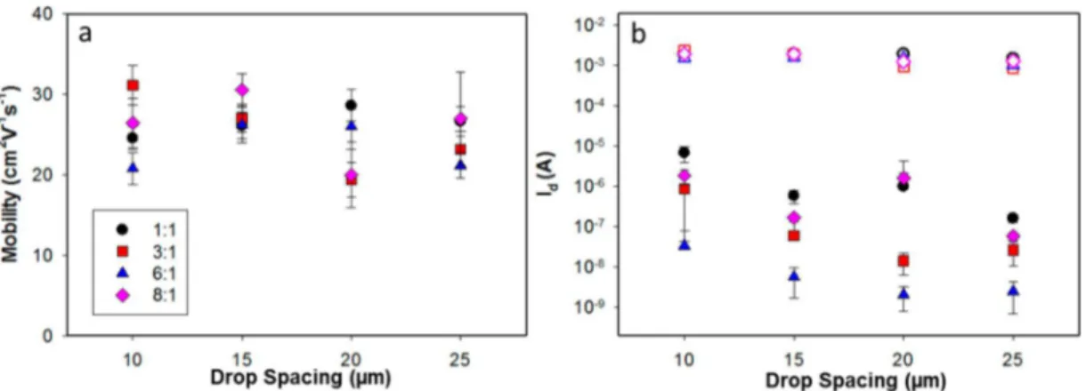
2.3. Effect of PFDD:SWCNT Ratio. To examine the effect of PFDD to SWCNT ratio on TFT performance, channels were printed using the 50 mg L−1 SWCNT ink with PFDD:SWCNT ratios of 1:1, 3:1, 6:1, and 8:1. As the polymer to nanotube ratio was increased, improved jetting was realized. The resulting TFT performance was measured (Figure 5). Mobility values range between approximately 20 and 30 cm2 V−1s−1, with no clear trend with drop spacing or polymer ratio. Similarly there was little variation in the on-current. In contrast,
significant differences are observed in the off-currents. As the amount of PFDD is increased from 1:1 to 3:1 to 6:1, there is a steady decrease in the off-current regardless of drop spacing. The origin of this effect requires further investigation, but the results may suggest the higher polymer ratio inks (up to 6:1) lead to less bundling in the resulting SWCNT networks. Increasing the polymer ratio to 8:1 yields no further benefit, in fact the off-current increased relative to the 6:1 data.
On the basis of the results discussed above, the optimal PFDD to SWCNT ratio was determined to be 6:1. The optimal PFDD/SWCNT ink formulation (50 mg L−1; 6:1 ratio) at a drop spacing of 20 μm resulted in a mobility of ∼25 cm2V−1 s−1 with an on/off ratio of >105, which is consistent with previously reported TFTs prepared by solution casting PFDD/ SWCNTs19 indicating there is no significant loss of perform-ance associated with the inkjet printing process. The results here also compare favorably with that observed with printed SWCNT channels on SiO2 using aqueous dispersions of SWCNTs.14
2.4. Long Channel TFTs with Inkjet Printed Source/ Drain Contacts.Devices with a practical channel length (L = 125 μm; W = 200 μm) for mass production47via R2R printing were inkjet printed using the optimal SWCNT ink and deposition conditions on SiO2/Si substrates (50 mg L−1, PFDD:SWCNT ratio of 6:1 at a drop spacing of 20 μm). The TFTs were then completed by inkjet printing source/drain contacts using silver nanoparticle ink. Device performance
Figure 5.(a) Mobility and (b) on- (empty) and off-currents (filled) for the 20 μm × 2000 μm channels printed with 50 mg L−1PFDD/SWCNT ink
on Si test chips (90 nm SiO2gate dielectric and evaporated Ti/Au bottom contacts) as a function of drop spacing for different polymer to nanotube
ratios.
Figure 6.Transfer (a) at Vds= −1 V and (b) output characteristics of a TFT with inkjet printed PFDD/SWCNT (50 mg L−1, 6:1) channel and
inkjet printed silver source/drain top contacts (L = 125 μm, W = 200 μm) on SiO2(100 nm)/Si substrate (where, for example, 1.E-04 represents 1.0
×10−4).
DOI:10.1021/acsami.6b06838
ACS Appl. Mater. Interfaces XXXX, XXX, XXX−XXX
characteristics serve as a basis for comparison with fully printed devices (vide infra) having comparable channel lengths (Figure 6). From the transfer curve, the on/off ratio is estimated to be >2 × 10⁵with a subthreshold swing of 1.9 V decade−1. Linear fits to the curve yield a transconductance of 1.8 μS V−1and a threshold voltage of −6.5 V. The resulting mobility is 33 cm2 V−1s−1. The output characteristics show on-currents of ∼0.37 mA mm−1 in saturation at Vg = −10 V. This device performance compares favorably with that obtained on the shorter channel devices discussed above and establishes that the increased channel length and printed top contacts are not factors that limit the TFT performance on SiO2/Si.
2.5. Fully Printed SWCNT Flexible Transistors.Building on the optimal SWCNT ink formulation and printing process, fully printed transistors on flexible plastic substrates were manufactured exclusively using additive manufacturing, specif-ically combining inkjet printing with R2R gravure printing. A flexible polyethylene terephthalate (PET) substrate had silver gate electrodes and high-k BaTiO3 dielectric layers consec-utively printed via a R2R gravure printing process.29 The printed stack was subjected to argon plasma followed by inkjet printing of 50 mg L−1SWCNT ink (6:1 PFDD:SWCNT ratio). After printing, the substrates were heated to improve SWCNT adhesion, followed by rinsing and baking. To complete the TFTs, silver source/drain contacts were inkjet printed and photosintered, defining a channel of 1000 μm × 150 μm. It is important to note the stability of the SWCNT network to high-intensity pulsed UV radiation used to sinter the silver nanoparticle inks.
Transfer and output characteristics of the resulting TFTs were measured (Figure 7). From the transfer curve the on/off ratio was determined to be ∼7 × 10⁴with a subthreshold swing of 1.8 V decade−1. Linear fits to the transfer curve yield a transconductance of 0.26 μS V−1 and a threshold voltage of −2.5 V. Using the measured average thickness of the dielectric (2.3 μm) and the quoted dielectric constant (k = 17),29yields a calculated capacitance of 6.5 nF cm−2. The resulting mobility (extracted via the parallel plate model) is 6 cm2V−1s−1. The output characteristics show on-currents of ∼0.1 mA mm−1in saturation. Although the fully printed devices are an order of magnitude lower mobility than those on Si/SiO2, the device performance compares favorably with that obtained previously from top gated devices involving SWCNT channels combined with the sheet-to-sheet gravure printed dielectric and electrode layers. In that case, aqueous dispersions of SWCNTs were used
to produce SWCNT networks onto polylysine coated PET via soaking, followed by printing of the source/drain, dielectric, and gate electrode layers. In that study, the average mobility of 66 TFTs was reported as 4.3 ± 1.6 cm2V−1s−1with an average on/off ratio of 3.5 × 10⁴and a threshold voltage of −2.3 ± 1.2 V.29The distinguishing feature when compared to the present work is herein the channel that was spatially defined by inkjet printing, thus enabling a fully additive process. Furthermore, consistent performance is achieved via a single pass to print the channel, providing an efficient process without loss of performance. Further comparing these additive manufactured TFTs to fully gravure printed TFTs using unsorted SWCNTs as the channel material, an order of magnitude improvement in mobility was achieved.42
One possible explanation for the reduced mobility on the fully printed devices (compared with those on SiO2) is a lower SWCNT network density. This hypothesis was tested by Raman microscopy, using the intensity of SWCNT features to estimate the tube density on the surface, as was done for the devices on SiO2. Based on the ink concentration, drop volume, and spacing, the amount of SWCNTs deposited onto the flexible printed stack was estimated to be ∼2000 μm−2. After rinsing with toluene, 60−85% of SWCNTs remain on the surface (Figure S5) indicating the network density in these devices is quite high. SEM images in the channel region of these fully printed devices (Figure S6) also indicate a high density of SWCNTs. These measurements indicate that the network density of these devices is comparable (perhaps slightly greater than) to that on SiO2, so other factors such as surface roughness and nonuniform network morphology are needed to account for the lower mobility. In fact, the large surface roughness (∼10 nm) of the printed BTO dielectric likely plays a significant role in charge trap formation.3,4,47
SWCNT TFTs have been shown to be highly sensitive to their surrounding environment with a chemical redox reaction involving adsorbed water leading to hysteresis and threshold voltage shifts in the transfer characteristics.44,48 Thus, fabrication of TFTs that can serve as building blocks for printable circuits will require a strategy for encapsulation to minimize these effects. Recently, it has been demonstrated that a commercially available solution processable PVP/PMSSQ-based dielectric (xdi-d1.2) can be used to encapsulate SWCNT TFTs resulting in hysteresis-free operation and devices that are “off” in the absence of gate bias (i.e. enhancement mode operation).49 This motivated the encapsulation of the fully
Figure 7.Transfer (a) at Vds= −1 V and (b) output characteristics for a TFT with inkjet printed PFDD/SWCNT (50 mg L−1, 6:1) channels and
silver source/drain electrodes on a PET substrate with gravure printed silver gate and BaTiO3−polymer composite dielectric layers (where, for
example, -2.0e-5 represents −2.0 × 10⁻⁵). An optical image of a fully printed TFT is shown in the inset; device dimensions are 1000 μm × 150 μm.
DOI:10.1021/acsami.6b06838
ACS Appl. Mater. Interfaces XXXX, XXX, XXX−XXX
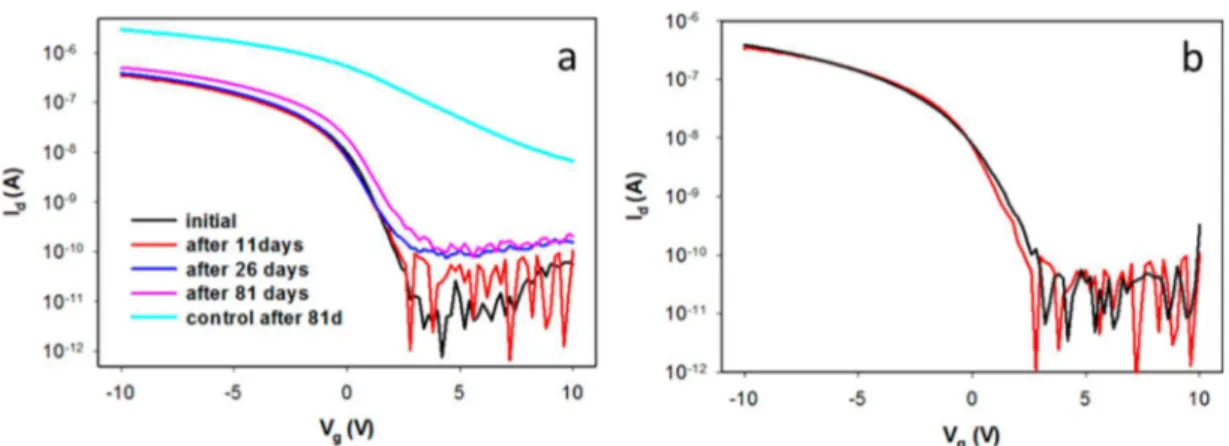
printed flexible devices via inkjet printing several layers of PVP/ PMSSQ. Printing the dielectric as an encapsulation layer on-top of the completed TFT has the beneficial effects of lowering the off-currents and stabilizing the transfer characteristics (Figure 8). Monitoring these devices for an extended period of time revealed that the transfer curves remain largely unchanged for almost 1 month, and show only slight changes (apart from a significant increase in off-current) after almost 3 months storage under ambient conditions. In contrast, the TFTs that are left bare and exposed to the same ambient conditions and time period exhibit increased currents but also threshold voltages shifting to positive voltage and an increase in the
subthreshold slope. The encapsulated devices also exhibit minimal hysteresis (<0.2 V) for voltage sweeps of ±10 V.
The increased stability and improved on/off ratio due to encapsulation by the dielectric comes at the cost of current and mobility (transconductance decrease of ∼2−3 times). For example, a device prior to encapsulation had transconductance of 128 nS V−1, whereas after encapsulation it decreased to 41 nS V−1(Figure 8). This decrease likely reflects a combination of some disruption of the SWCNT network as well as exclusion of ambient water which acts to enhance the p-channel conduction.44 Minimal variation of less than 10% of the transconductance and threshold voltage was observed after 26 days; however, the off-current increased by an order of
Figure 8. (a) Effect of storage in ambient conditions (humidity of 40−60%; T ∼ 25 °C) on the transfer characteristics of SWCNT TFTs encapsulated with an inkjet printed dielectric (PVP/PMSSQ) overlayer (∼3 μm thick). The transfer characteristic for a non-encapsulated device on the same substrate, exposed to the same ambient, is shown as a control. (b) Transfer characteristics for an encapsulated device obtained by sweeping the voltage to positive voltages (red) and negative voltages (black) demonstrates minimal hysteresis (see Figure S7 for linear fits to transfer characteristics).
Figure 9. (a) Transfer characteristics for 20 fully printed, encapsulated SWCNT TFTs on a PET substrate. (b) Schematic showing how the encapsulated SWCNT-TFTs were measured as an inverter by using an external load resistor (∼2 MΩ). (c) Results of output digital signals (red trace) by inputting digital signal “0” and “1” with 10 Hz square wave (black trace) into the inverter.
DOI:10.1021/acsami.6b06838
ACS Appl. Mater. Interfaces XXXX, XXX, XXX−XXX
magnitude during this time. After 81 days, more significant changes are observed with the threshold voltage shifting from −1.4 V to −0.7 V and transconductance increasing from 41 nS V−1 to 54 nS V−1. In contrast, much larger changes in the transfer characteristics are observed for the bare devices, where the on- and off-currents are seen to increase substantially, the threshold voltage shifts to positive voltage (+1.9 V) and the turn-on of the device becomes much more gradual (subthres-hold swing increases). Analysis of devices encapsulated with different thicknesses of dielectric indicate an inverse correlation between threshold voltage shifts with time and the thickness of the dielectric (Figure S8), strongly suggesting that penetration of ambient species through the encapsulation layer are responsible for the observed shifts over time.
Evaluating the suitability of a process to encapsulate printed SWCNT TFTs that are intended to be used as building blocks for logic circuits requires some assessment of the device to device variation and the stability of output signals. One method of assessing stability is by monitoring the output of a printed inverter circuit in response to digital (“0” and “1”) input signals.4,42,50Variation will dictate the complexity of a circuit that can be realized with the present process technology and determine the suitability of printed TFTs in the target application.4,42,50 Transfer curves from 20 encapsulated fully printed devices along a row show minimal variation (Figure 9a). The fully printed encapsulated device was used to construct an inverter (Figure 9b) to show constant output voltage levels in digital signals (Figure 9c) because monitoring the variation level of the output voltage during operation of the printed logic gate (inverter) is a very accurate and practical assessment tool to construct logic circuits (Figures S9 and S10). The encapsulated SWCNT TFT-based inverter can maintain a constant level of output digital signal during a continuous operation time of 140 min (Figure 9c).
Furthermore, variability in four important TFT performance parameters extracted from these transfer curves was evaluated. Bar graphs of the threshold voltage, transconductance, on-current, and subthreshold swing show that most of the 20
devices exhibit variability within ±10%, with the remainder being just outside this range (Figure 10). The measured transconductance corresponds to a mobility of 1.3 ± 0.1 cm2 V−1 s−1 using the estimated capacitance of 6.5 nF cm−2. Recently, Monte Carlo simulations have shown that functional circuits with reasonable complexity, such as a full adder, can be printed with 76% yield when threshold voltage variation is limited to less than 30%.42These results strongly indicate that the process reported here can be used to construct practical devices including logic circuits with improved mobility and on-currents and can further expand the application space in printed electronics.4,50
3. CONCLUSIONS
In this work the optimal ink formulation and processes for inkjet printing were identified for dispersions of SWCNTs produced by a hybrid extraction/adsorption process23using a polyfluorene derivative (PFDD). The effects of SWCNT concentration, the volume of ink deposited, and the ratio of PFDD to SWCNT on TFT performance obtained on rigid Si/ SiO2-based test chips have been examined. Inks formulated at a SWCNT concentration of 50 mg L−1and a PFDD to SWCNT ratio of 6:1 were found to be optimal in terms of maximizing both device performance and jetting reliability. TFTs with inkjet printed PFDD/SWCNT channels on SiO2 are demonstrated to exhibit effective mobilities of ∼30 cm2 V−1s−1and on/off ratios of ∼105, similar to what is obtained by solution casting.23The optimal ink formulation and printing process developed on these test chips has then been applied to the fully additive fabrication of all-printed TFTs on a flexible PET substrate utilizing R2R gravure and inkjet printing. These fully printed devices show mobilities of up to 6 cm2 V−1 s−1 with an on/off ratio of 7 × 10⁴, showing the promise of ink formulations based on PFDD separated SWCNTs for inkjet printing of TFT channels. Devices encapsulated with a PVP/ PMSSQ polymer dielectric overlayer exhibit somewhat lower mobilities (1−2 cm2V−1s−1) with minimal hysteresis and good device stability. The results reported here represent an
Figure 10.Bar graphs showing variations in threshold voltage, transconductance, on-current (Vds= −1 V, Vg= −9 V) and subthreshold slopes,
extracted for the 20 fully printed TFTs whose transfer curves are shown inFigure 9. The solid lines represent the average value while the dashed lines indicate ±10% variations from this average.
DOI:10.1021/acsami.6b06838
ACS Appl. Mater. Interfaces XXXX, XXX, XXX−XXX
important practical step forward in the development of fully additive processes for the realization of all-printed flexible TFTs based on semiconducting SWCNT channels.
4. EXPERIMENTAL SECTION
4.1. Materials.Semiconducting enriched SWCNTs dispersed with poly(9,9-di-n-dodecylfluorene) (PFDD)23 were purchased from Raymor NanoIntegris (IsoSol-S100 powder, PFDD:SWCNT weight ratio of 1:1). Additional PFDD used to formulate inks with various PFDD:SWCNT ratios was synthesized as described previously.19For
inkjet printing, poly(vinylphenol) (PVP; dielectric constant, κ = 4.0) based dielectric/encapsulant ink, with low surface tension additive poly(methyl silsesquioxane) (PVP/PMSSQ), was purchased from Xerox Research Center Canada (product name, xdi-d1.2). PVP/ PMSSQ was formulated as an encapsulation ink for inkjet printing using butanol. Silver nanoparticle ink (ANP DGP-HRA) for source/ drain electrodes was purchased from Advanced Nano Products (ANP). Highly p-doped Si wafer with thermally grown 100 nm of SiO2was purchased from SQI and used as a substrate for the feasibility
study of long channel devices with inkjet printed silver source/drain electrodes. For R2R gravure printing, high-k BaTiO3-based dielectric
ink (PD-100) was purchased from PARU Co. Korea and silver nanoparticle ink (PG-007) was purchased from PARU. Silicon-based test chips prepatterned with arrays of 16 transistors (channel width = 2 mm; channel lengths, L = 2.5, 5, 10, and 20 μm) consisting of 30 nm thick interdigitated Au source/drain electrodes over 90 nm thermally grown SiO2 were purchased from Fraunhofer IPMS. Poly(ethylene
terephthalate) (PET) film roll (100 μm thick by 250 mm wide) was purchased from SKC, Korea. All other reagents and solvents were purchased from Sigma-Aldrich and used as received. Sonication was performed using a Branson 8891 sonicating bath equipped with an auxiliary pan. Plasma cleaning was performed using Yield Engineering Systems G-500. A Fujifilm Dimatix DMP-2831 inkjet printer equipped with a 10 pL print head was used for inkjet deposition. Photonic sintering was performed using a Xenon Sinteron S2000.
4.2. SWCNT Ink Preparation. A 20 mL scintillation vial was charged with 4.0 mg of IsoSol-S100 powder and 18 mL of toluene. The solution was sonicated for 30 min. The resulting dark solution (96 mg L−1SWCNT) was then diluted with toluene to achieve the desired
concentration. The polymer ratio was modified by adding an appropriate mass of PFDD to the desired concentration of SWCNT solution. For example, 1.0 mg of PFDD was added to 3 mL of a 50 mg L−1SWCNT solution with a PFDD:SWCNT ratio of 1:1 to obtain a
solution with a polymer ratio of 8:1. The concentration and polymer ratio were confirmed using absorption spectroscopy.19
4.3. SWCNT Transistor Preparation on Test Chips. Each silicon-based test chip was rinsed with acetone to remove the protective photoresist layer, then rinsed with isopropanol and deionized water, and subsequently dried under a stream of N2 gas.
The chip was plasma cleaned for 2.5 min at 400 W, with 50 cm3(STP)
min−1 oxygen flow rate. The chip was then rotated 90° and
repositioned for an additional 2.5 min of plasma cleaning under the same conditions. Cleaned chips were immediately placed in the inkjet printer with the platen at 28 °C. SWCNT ink was deposited by inkjet printing using an optimized print waveform at the selected drop spacing in a 400 μm × 1200 μm rectangular pattern to cover the desired active channel area between and overlapping the source/drain electrodes. Finally, after the ink was dry, the chip was rinsed under a stream of toluene for 40 s, dried under a stream of nitrogen, and baked for 10 min at 150 °C to complete the device processing. For multiple layer prints, the silicon chips were only rinsed and baked after all layers had been printed.
4.4. SWCNT Transistor Preparation on SiO2 Wafers. Each
silicon wafer (100 nm SiO2) was rinsed with isopropanol and
subsequently dried under a stream of N2 gas. The wafer was placed
onto a 50 °C platen within the printer and alignment marks were deposited onto the surface by inkjet printing silver ink with 40 μm drop spacing. Subsequently, the wafer was placed onto a hot plate at 75 °C for 15 min to dry the ink before curing the ink at 140 °C for 30
min in an oven. The wafer was then plasma cleaned for 2.5 min at 400 W, with 50 cm3(STP) min−1oxygen, rotated 90° and repositioned for
a subsequent 2.5 min of plasma cleaning. Cleaned wafers were immediately placed in the inkjet printer with the platen at 28 °C. SWCNT ink was deposited by inkjet printing using an optimized print waveform at 20 μm drop spacing in a 125 μm × 200 μm rectangular pattern to prepare the active channel area. Following printing and the ink drying, the wafer was rinsed under a stream of toluene for 40 s, dried under a stream of nitrogen, and baked for 15 min at 150 °C to complete the device processing. Silver source/drain contacts were inkjet printed at 25 μm drop spacing and at 28 °C and dried on a hot plate at 75 °C for 15 min followed by curing at 140 °C for 20 min.
4.5. Characterization of SWCNT Transistor on SiO2. After
processing, TFT performance was measured on a probe station in ambient conditions, using the back of the highly doped n-type silicon substrate as a common bottom gate electrode for all TFTs on a test chip. Keithley 2400 source-measure units were used to measure transfer and output characteristics of the TFTs. Field effect mobilities were extracted from measured transfer characteristics in the linear region (Vds= −1 V) using the parallel plate model for the capacitance
(Cox = 38 nF cm−2). Use of this model for the capacitance likely
underestimates the actual mobility as it overestimates the capaci-tance;51 however it does not require an accurate estimate of the
SWCNT network density.
4.6. Fully Printed and Encapsulated SWCNT Transistor Preparation Combining Inkjet and R2R Gravure Printing. Using the previously reported R2R gravure printing process29 silver gate electrode and BaTiO3composite dielectric layers were printed on
a PET substrate. The gravure printed PET film was subsequently plasma treated for 5 min at 100 W, 50 cm3(STP) min−1 of argon
followed by inkjet printing at 15 μm drop spacing the 50 mg L−1
SWCNT ink (6:1 PFDD:SWCNT ratio) as the channel material at 28 °C. After printing, the substrates were heated on a hot plate at 75 °C for 15 min, rinsed with toluene, and baked at 140 °C for 10 min. Silver source/drain contacts were inkjet printed at 25 μm drop spacing and at 28 °C, dried on a hot plate at 80 °C for 10 min followed by photonic sintering with a 0.5 ms pulse width at 2.4 kV. Encapsulated devices were obtained by inkjet printing the PVP/PMSSQ encapsulant onto the exposed channel at a 20 μm drop spacing and at 28 °C.
■
ASSOCIATED CONTENT*
S Supporting InformationThe Supporting Information is available free of charge on the
ACS Publications websiteat DOI:10.1021/acsami.6b06838. Additional electrical data, Raman data, details of inverter measurements, SEM images, and printing images (PDF)
■
AUTHOR INFORMATION Corresponding Authors *(C.M.H.) E-mail:christa.homenick@nrc-cnrc.gc.ca. *(P.R.L.M.) E-mail:patrick.malenfant@nrc-cnrc.gc.ca. *(G.C.) E-mail:gcho@sunchon.ac.kr. NotesThe authors declare no competing financial interest.
■
ACKNOWLEDGMENTSWe are pleased to acknowledge Dr. Jacques Lefebvre and Jeff Fraser for SEM imaging. We are pleased to acknowledge Dr. Jianfu Ding and Dr. Zhao Li for valuable discussions regarding the SWCNT ink formulation. G.C. thanks the Global Leading Technology Program of the Office of Strategic R&D Planning (OSP) funded by the Ministry of Commerce, Industry and Energy, Republic of Korea (Grant 10042537, Printed Electronics Total Solution Development).
DOI:10.1021/acsami.6b06838
ACS Appl. Mater. Interfaces XXXX, XXX, XXX−XXX
■
REFERENCES(1) Subramanian, V.; Chang, J. B.; Vornbrock, A. d. l. F.; Huang, D. C.; Jagannathan, L.; Liao, F.; Mattis, B.; Molesa, S.; Redinger, D. R.; Soltman, D.; Volkman, S. K.; Zhang, Q. . Solid-State Device Research Conference (ESSDERC), 38th European; IEEE: New York, 2008; Vol. 34, pp 17−24.10.1109/ESSDERC.2008.4681691
(2) Perelaer, J.; Smith, P. J.; Mager, D.; Soltman, D.; Volkman, S. K.; Subramanian, V.; Korvink, J. G.; Schubert, U. S. Printed Electronics: The Challenges Involved in Printing Devices, Interconnects, and Contacts Based on Inorganic Materials. J. Mater. Chem. 2010, 20 (39), 8446−8453.
(3) Jung, M.; Kim, J.; Noh, J.; Lim, N.; Lim, C.; Lee, G.; Kim, J.; Kang, H.; Jung, K.; Leonard, A. D.; Tour, J. M.; Cho, G. All-Printed and Roll-to-Roll-Printable Tag on Plastic Foils. IEEE Trans. Electron Devices 2010, 57 (3), 571−580.
(4) Noh, J.; Jung, M.; Jung, Y.; Yeom, C.; Pyo, M.; Cho, G. Key Issues With Printed Flexible Thin Film Transistors and Their Application in Disposable RF Sensors. Proc. IEEE 2015, 103 (4), 554−566.
(5) Cao, Q.; Rogers, J. A. Ultrathin Films of Single-Walled Carbon Nanotubes for Electronics and Sensors: A Review of Fundamental and Applied Aspects. Adv. Mater. 2009, 21 (1), 29−53.
(6) Jariwala, D.; Sangwan, V. K.; Lauhon, L. J.; Marks, T. J.; Hersam, M. C. Carbon Nanomaterials for Electronics, Optoelectronics, Photovoltaics, and Sensing. Chem. Soc. Rev. 2013, 42 (7), 2824−2860. (7) Cai, L.; Wang, C. Carbon Nanotube Flexible and Stretchable Electronics. Nanoscale Res. Lett. 2015, 10 (1), 320−341.
(8) Zaumseil, J. Single-Walled Carbon Nanotube Networks for Flexible and Printed Electronics. Semicond. Sci. Technol. 2015, 30 (7), 074001−074021.
(9) Beecher, P.; Servati, P.; Rozhin, A.; Colli, A.; Scardaci, V.; Pisana, S.; Hasan, T.; Flewitt, A. J.; Robertson, J.; Hsieh, G. W.; Li, F. M.; Nathan, A.; Ferrari, A. C.; Milne, W. I. Ink-Jet Printing of Carbon Nanotube Thin Film Transistors. J. Appl. Phys. 2007, 102 (4), 043710−043717.
(10) Vaillancourt, J.; Zhang, H.; Vasinajindakaw, P.; Xia, H.; Lu, X.; Han, X.; Janzen, D. C.; Shih, W.-S. S.; Jones, C. S.; Stroder, M.; Chen, M. Y.; Subbaraman, H.; Chen, R. T.; Berger, U.; Renn, M. All Ink-Jet-Printed Carbon Nanotube Thin-Film Transistor on a Polyimide Substrate with an Ultrahigh Operating Frequency of over 5 GHz. Appl. Phys. Lett. 2008, 93 (24), 243301.
(11) Okimoto, H.; Takenobu, T.; Yanagi, K.; Miyata, Y.; Shimotani, H.; Kataura, H.; Iwasa, Y. Tunable Carbon Nanotube Thin-Film Transistors Produced Exclusively via Inkjet Printing. Adv. Mater. 2010, 22 (36), 3981−3986.
(12) Arnold, M. S.; Stupp, S. I.; Hersam, M. C. Enrichment of Single-Walled Carbon Nanotubes by Diameter in Density Gradients. Nano Lett. 2005, 5 (4), 713−718.
(13) Arnold, M. S.; Green, A. a; Hulvat, J. F.; Stupp, S. I.; Hersam, M. C. Sorting Carbon Nanotubes by Electronic Structure Using Density Differentiation. Nat. Nanotechnol. 2006, 1 (1), 60−65.
(14) Chen, P.; Fu, Y.; Aminirad, R.; Wang, C.; Zhang, J.; Wang, K.; Galatsis, K.; Zhou, C. Fully Printed Separated Carbon Nanotube Thin Film Transistor Circuits and Its Application in Organic Light Emitting Diode Control. Nano Lett. 2011, 11, 5301−5308.
(15) Liu, H.; Nishide, D.; Tanaka, T.; Kataura, H. Large-Scale Single-Chirality Separation of Single-Wall Carbon Nanotubes by Simple Gel Chromatography. Nat. Commun. 2011, 2 (May), 309−317.
(16) Khripin, C. Y.; Fagan, J. a; Zheng, M. Spontaneous Partition of Carbon Nanotubes in Polymer-Modified Aqueous Phases. J. Am. Chem. Soc. 2013, 135 (18), 6822−6825.
(17) Fagan, J. a.; Khripin, C. Y.; Silvera Batista, C. a.; Simpson, J. R.; Hároz, E. H.; Hight Walker, A. R.; Zheng, M. Isolation of Specific Small-Diameter Single-Wall Carbon Nanotube Species via Aqueous Two-Phase Extraction. Adv. Mater. 2014, 26 (18), 2800−2804.
(18) Lee, H. W.; Yoon, Y.; Park, S.; Oh, J. H.; Hong, S.; Liyanage, L. S.; Wang, H.; Morishita, S.; Patil, N.; Park, Y. J.; Park, J. J.; Spakowitz, A.; Galli, G.; Gygi, F.; Wong, P. H.-S.; Tok, J. B.-H.; Kim, J. M.; Bao, Z. Selective Dispersion of High Purity Semiconducting Single-Walled
Carbon Nanotubes with Regioregular poly(3-Alkylthiophene)s. Nat. Commun. 2011, 2, 541−548.
(19) Ding, J.; Li, Z.; Lefebvre, J.; Cheng, F.; Dubey, G.; Zou, S.; Finnie, P.; Hrdina, A.; Scoles, L.; Lopinski, G. P.; Kingston, C. T.; Simard, B.; Malenfant, P. R. L. Enrichment of Large-Diameter Semiconducting SWCNTs by Polyfluorene Extraction for High Network Density Thin Film Transistors. Nanoscale 2014, 6 (4), 2328−2339.
(20) Schießl, S. P.; Frohlich, N.; Held, M.; Gannott, F.; Schweiger, M.; Forster, M.; Scherf, U.; Zaumseil, J. Polymer-Sorted Semi-conducting Carbon Nanotube Networks for High-Performance Ambipolar Field-Effect Transistors. ACS Appl. Mater. Interfaces 2015, 7, 682−689.
(21) Xu, W.; Zhao, J.; Qian, L.; Han, X.; Wu, L.; Wu, W.; Song, M.; Zhou, L.; Su, W.; Wang, C.; Nie, S.; Cui, Z. Sorting of Large-Diameter Semiconducting Carbon Nanotube and Printed Flexible Driving Circuit for Organic Light Emitting Diode (OLED). Nanoscale 2014, 6, 1589−1595.
(22) Homenick, C. M.; Rousina-Webb, A.; Cheng, F.; Jakubinek, M. B.; Malenfant, P. R. L.; Simard, B. High-Yield, Single-Step Separation of Metallic and Semiconducting SWCNTs Using Block Copolymers at Low Temperatures. J. Phys. Chem. C 2014, 118, 16156−16164.
(23) Ding, J.; Li, Z.; Lefebvre, J.; Cheng, F.; Dunford, J. L.; Malenfant, P. R. L.; Humes, J.; Kroeger, J. A Hybrid Enrichment Process Combining Conjugated Polymer Extraction and Silica Gel Adsorption for High Purity Semiconducting Single-Walled Carbon Nanotubes (SWCNT). Nanoscale 2015, 7 (38), 15741−15747.
(24) Sangwan, V. K.; Ortiz, R. P.; Alaboson, J. M. P.; Emery, J. D.; Bedzyk, M. J.; Lauhon, L. J.; Marks, T. J.; Hersam, M. C. Fundamental Performance Limits of Carbon Nanotube Thin-Film Transistors Achieved Using Hybrid Molecular Dielectrics. ACS Nano 2012, 6, 7480−7488.
(25) Geier, M. L.; Prabhumirashi, P. L.; McMorrow, J. J.; Xu, W.; Seo, J. W. T.; Everaerts, K.; Kim, C. H.; Marks, T. J.; Hersam, M. C. Subnanowatt Carbon Nanotube Complementary Logic Enabled by Threshold Voltage Control. Nano Lett. 2013, 13 (10), 4810−4814.
(26) Higuchi, K.; Kishimoto, S.; Nakajima, Y.; Tomura, T.; Takesue, M.; Hata, K.; Kauppinen, E. I.; Ohno, Y. High-Mobility, Flexible Carbon Nanotube Thin-Film Transistors Fabricated by Transfer and High-Speed Flexographic Printing Techniques. Appl. Phys. Express 2013, 6 (8), 085101−1−4.
(27) Rouhi, N.; Jain, D.; Zand, K.; Burke, P. J. Fundamental Limits on the Mobility of Nanotube-Based Semiconducting Inks. Adv. Mater. 2011, 23 (1), 94−99.
(28) Wang, C.; Chien, J.-C.; Takei, K.; Takahashi, T.; Nah, J.; Niknejad, A. M.; Javey, A. Extremely Bendable, High-Performance Integrated Circuits Using Semiconducting Carbon Nanotube Net-works for Digital, Analog, and Radio-Frequency Applications. Nano Lett. 2012, 12 (3), 1527−1533.
(29) Lau, P. H.; Takei, K.; Wang, C.; Ju, Y.; Kim, J.; Yu, Z.; Takahashi, T.; Cho, G.; Javey, A. Fully Printed, High Performance Carbon Nanotube Thin-Film Transistors on Flexible Substrates. Nano Lett. 2013, 13 (8), 3864−3869.
(30) Cai, L.; Zhang, S.; Miao, J.; Yu, Z.; Wang, C. Fully Printed Foldable Integrated Logic Gates with Tunable Performance Using Semiconducting Carbon Nanotubes. Adv. Funct. Mater. 2015, 25 (35), 5698−5705.
(31) Cao, X.; Chen, H.; Gu, X.; Liu, B.; Wang, W.; Cao, Y.; Wu, F.; Zhou, C. Screen Printing as a Scalable and Low-Cost Approach for Rigid and Flexible Thin-Film Transistors Using Separated Carbon Nanotubes. ACS Nano 2014, 8 (12), 12769−12776.
(32) Wang, H.; Wei, P.; Li, Y.; Han, J.; Lee, H. R.; Naab, B. D.; Liu, N.; Wang, C.; Adijanto, E.; Tee, B. C.-K.; Morishita, S.; Li, Q.; Gao, Y.; Cui, Y.; Bao, Z. Tuning the Threshold Voltage of Carbon Nanotube Transistors by N-Type Molecular Doping for Robust and Flexible Complementary Circuits. Proc. Natl. Acad. Sci. U. S. A. 2014, 111 (13), 4776−4781.
(33) Lee, C. W.; Raman Pillai, S. K.; Luan, X.; Wang, Y.; Li, C. M.; Chan-Park, M. B. High-Performance Inkjet Printed Carbon Nanotube
DOI:10.1021/acsami.6b06838
ACS Appl. Mater. Interfaces XXXX, XXX, XXX−XXX
Thin Film Transistors with High-K HfO(2) Dielectric on Plastic Substrate. Small 2012, 8 (19), 2941−2947.
(34) Noh, J.; Jung, M.; Jung, K.; Lee, G.; Lim, S.; Kim, D.; Kim, S.; Tour, J. M.; Cho, G. Integrable Single Walled Carbon Nanotube (SWNT) Network Based Thin Film Transistors Using Roll-to-Roll Gravure and Inkjet. Org. Electron. 2011, 12 (12), 2185−2191.
(35) Zhao, J.; Gao, Y.; Gu, W.; Wang, C.; Lin, J.; Chen, Z.; Cui, Z. Fabrication and Electrical Properties of All-Printed Carbon Nanotube Thin Film Transistors on Flexible Substrates. J. Mater. Chem. 2012, 22 (38), 20747−20754.
(36) Kim, B.; Geier, M. L.; Hersam, M. C.; Dodabalapur, A. Inkjet Printed Circuits on Flexible and Rigid Substrates Based on Ambipolar Carbon Nanotubes with High Operational Stability. ACS Appl. Mater. Interfaces 2015, 7 (50), 27654−27660.
(37) Ha, M.; Xia, Y.; Green, A. a.; Zhang, W.; Renn, M. J.; Kim, C. H.; Hersam, M. C.; Frisbie, C. D. Printed, Sub-3V Digital Circuits on Plastic from Aqueous Carbon Nanotube Inks. ACS Nano 2010, 4 (8), 4388−4395.
(38) Ha, M.; Seo, J.-W. T. W. T.; Prabhumirashi, P. L.; Zhang, W.; Geier, M. L.; Renn, M. J.; Kim, C. H.; Hersam, M. C.; Frisbie, C. D. Aerosol Jet Printed, Low Voltage, Electrolyte Gated Carbon Nanotube Ring Oscillators with Sub-5 μs Stage Delays. Nano Lett. 2013, 13 (3), 954−960.
(39) Liu, Z.; Zhao, J.; Xu, W.; Qian, L.; Nie, S.; Cui, Z. Effect of Surface Wettability Properties on the Electrical Properties of Printed Carbon Nanotube Thin-Film Transistors on SiO2/Si Substrates. ACS Appl. Mater. Interfaces 2014, 6, 9997−10004.
(40) Li, H.; Tang, Y.; Guo, W.; Liu, H.; Zhou, L.; Smolinski, N. Polyfluorinated Electrolyte for Fully Printed Carbon Nanotube Electronics. Adv. Funct. Mater. 2016,DOI: 10.1002/adfm.201601605. (41) Noh, J.; Jung, M.; Jung, K.; Lee, G.; Kim, J.; Lim, S.; Kim, D.; Choi, Y.; Kim, Y.; Subramanian, V.; Cho, G. Fully Gravure-Printed D Flip-Flop on Plastic Foils Using Single-Walled Carbon-Nanotube-Based TFTs. IEEE Electron Device Lett. 2011, 32 (5), 638−640.
(42) Koo, H.; Lee, W.; Choi, Y.; Sun, J.; Bak, J.; Noh, J.; Subramanian, V.; Azuma, Y.; Majima, Y.; Cho, G. Scalability of Carbon-Nanotube-Based Thin Film Transistors for Flexible Electronic Devices Manufactured Using an All Roll-to-Roll Gravure Printing System. Sci. Rep. 2015, 5, 14459−14470.
(43) Li, Z.; Ding, J.; Finnie, P.; Lefebvre, J.; Cheng, F.; Kingston, C. T.; Malenfant, R. L. Raman Microscopy Mapping for the Purity Assessment of Chirality Enriched Carbon Nanotube Networks in Thin Film Transistors. Nano Res. 2015, 8 (7), 2179−2187.
(44) Aguirre, C. M.; Levesque, P. L.; Paillet, M.; Lapointe, F.; St-Antoine, B. C.; Desjardins, P.; Martel, R. The Role of the Oxygen/ water Redox Couple in Suppressing Electron Conduction in Field-Effect Transistors. Adv. Mater. 2009, 21 (30), 3087−3091.
(45) Jung, Y.; Yeom, C.; Park, H.; Jung, D.; Koo, H.; Noh, J.; Wang, D.; Cho, G. Significant Effect of the Molecular Formula in Silver Nanoparticle Ink to the Characteristics of Fully Gravure-Printed Carbon Nanotube Thin-Film Transistors on Flexible Polymer Substrate. Org. Electron. 2016, 28, 197−204.
(46) Cao, C.; Andrews, J. B.; Kumar, A.; Franklin, A. D. Improving Contact Interfaces in Fully Printed Carbon Nanotube Thin-Film Transistors. ACS Nano 2016, 10, 5221−5229.
(47) Jung, Y.; Park, H.; Park, J.-A.; Noh, J.; Choi, Y.; Jung, M.; Jung, K.; Pyo, M.; Chen, K.; Javey, A.; Cho, G. Fully Printed Flexible and Disposable Wireless Cyclic Voltammetry Tag. Sci. Rep. 2015, 5, 8105− 8111.
(48) Li, H.; Zhou, L. Effects of Ambient Air and Temperature on Ionic Gel Gated Single-Walled Carbon Nanotube Thin-Film Transistor and Circuits. ACS Appl. Mater. Interfaces 2015, 7, 22881− 22887.
(49) Lefebvre, J.; Ding, J.; Li, Z.; Cheng, F.; Du, N.; Malenfant, P. R. L. Hysteresis Free Carbon Nanotube Thin Film Transistors Comprising Hydrophobic Dielectrics. Appl. Phys. Lett. 2015, 107, 243301.
(50) Lee, W.; Koo, H.; Sun, J.; Noh, J.; Kwon, K.-S.; Yeom, C.; Choi, Y.; Chen, K.; Javey, A.; Cho, G. A Fully Roll-to-Roll Gravure-Printed
Carbon Nanotube-Based Active Matrix for Multi-Touch Sensors. Sci. Rep. 2015, 5, 17707−17717.
(51) Cao, Q.; Xia, M.; Kocabas, C.; Shim, M.; Rogers, J. a.; Rotkin, S. V. Gate Capacitance Coupling of Singled-Walled Carbon Nanotube Thin-Film Transistors. Appl. Phys. Lett. 2007, 90, 023516.
DOI:10.1021/acsami.6b06838
ACS Appl. Mater. Interfaces XXXX, XXX, XXX−XXX