Publisher’s version / Version de l'éditeur:
Applied Physics Letters, 98, 13, pp. 132107-1-132107-3, 2011-04-01
READ THESE TERMS AND CONDITIONS CAREFULLY BEFORE USING THIS WEBSITE. https://nrc-publications.canada.ca/eng/copyright
Vous avez des questions? Nous pouvons vous aider. Pour communiquer directement avec un auteur, consultez la première page de la revue dans laquelle son article a été publié afin de trouver ses coordonnées. Si vous n’arrivez pas à les repérer, communiquez avec nous à PublicationsArchive-ArchivesPublications@nrc-cnrc.gc.ca.
Questions? Contact the NRC Publications Archive team at
PublicationsArchive-ArchivesPublications@nrc-cnrc.gc.ca. If you wish to email the authors directly, please see the first page of the publication for their contact information.
NRC Publications Archive
Archives des publications du CNRC
This publication could be one of several versions: author’s original, accepted manuscript or the publisher’s version. / La version de cette publication peut être l’une des suivantes : la version prépublication de l’auteur, la version acceptée du manuscrit ou la version de l’éditeur.
For the publisher’s version, please access the DOI link below./ Pour consulter la version de l’éditeur, utilisez le lien DOI ci-dessous.
https://doi.org/10.1063/1.3574540
Access and use of this website and the material on it are subject to the Terms and Conditions set forth at
Few-electron quantum dots in InGaAs quantum wells: Role of
fluctuations
Granger, G.; Studenikin, S. A.; Kam, A.; Sachrajda, A. S.; Poole, P. J.
https://publications-cnrc.canada.ca/fra/droits
L’accès à ce site Web et l’utilisation de son contenu sont assujettis aux conditions présentées dans le site LISEZ CES CONDITIONS ATTENTIVEMENT AVANT D’UTILISER CE SITE WEB.
NRC Publications Record / Notice d'Archives des publications de CNRC:
https://nrc-publications.canada.ca/eng/view/object/?id=0a72b3b1-1ee6-40bb-8853-06ecc881412a https://publications-cnrc.canada.ca/fra/voir/objet/?id=0a72b3b1-1ee6-40bb-8853-06ecc881412aFew-electron quantum dots in InGaAs quantum wells: Role of fluctuations
G. Granger,a兲S. A. Studenikin, A. Kam, A. S. Sachrajda, and P. J. Poole
Institute for Microstructural Sciences, National Research Council Canada, Ottawa, Ontario K1A 0R6, Canada
共Received 28 July 2010; accepted 17 March 2011; published online 1 April 2011兲
We study the electron transport properties of gated quantum dots formed in InGaAs/InP quantum well structures grown by chemical-beam epitaxy on prepatterned substrates. Quantum dots form directly underneath narrow gates due to potential fluctuations. We measure the Coulomb-blockade diamonds in the few-electron regime of a single dot and observe photon-assisted tunneling peaks under microwave irradiation. A singlet-triplet transition at high magnetic field and Coulomb-blockade in the quantum Hall regime are also observed. © 2011 American Institute of
Physics.关doi:10.1063/1.3574540兴
Materials with large spin-orbit coupling, such as InGaAs, are currently of considerable interest due to poten-tial spintronics applications. Although lateral quantum dots 共QDs兲 are routinely demonstrated in GaAs, the InGaAs material has not been suitable for this technology because of poor quality Schottky gates. Two groups have applied the split gate technique on InGaAs structures using dielectrics between the gates and the heterostructure.1,2 Prepatterned substrate technology allows to reduce leakage and exclude dielectrics, i.e., use Schottky gates rather than gates on di-electric. In addition, this technology is promising for optical applications and g-factor engineering.3 Here, we study the formation of single QDs in the few-electron regime in an InGaAs quantum well 共QW兲 under a narrow gate. We find that potential fluctuations play an important role in the for-mation of the QDs, as it was the case for incidental dots in GaAs.4–6 We perform a comprehensive study of these dots using standard magnetotransport techniques.
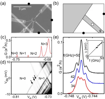
We start with a sample containing a 5 nm thick InGaAs QW in InP, 70 nm below the surface. NiAuGe Ohmic con-tacts are located on the edges of a 5 m wide active region. The split gate layout, similar to that of Ref. 7, is shown in Fig.1共a兲. Several devices had similar QD characteristics, and here we present one of them in which we have achieved the one-electron regime. As shown schematically in Fig. 1共b兲, the QD forms directly under the 160 nm wide gate labeled g, when the gate voltage Vg is brought close to the pinch-off
voltage. The remaining gates are biased passed their pinch-off to deplete the region in the upper left corner of Fig.1共b兲. As the electron density under gate g gradually decreases to zero, a small puddle of electrons survives as a result of a fluctuation in a similar way as reported in.4,5 We measure conductance G as a function of Vg at 0.3 K using standard
lock-in techniques. After illumination, the electron density in the ungated areas is 6 ⫻ 1015 m−2, and the mobility is
ⲏ2 m2/
V s, as estimated from two-terminal measurements. Figure 1共c兲 shows that Coulomb-blockade 共CB兲 peaks occur in the conductance as Vgis swept. The peak positions
change very little when the voltage on any other gate is changed 共ratio ⬃1 / 30, not shown兲, which confirms that the QD is formed under gate g. The CB peaks in Fig.1共c兲 cor-respond to charging of the last potential fluctuation.
In order to confirm that we operate in the few-electron regime, we apply a drain-source bias, Vds, and observe
typi-cal CB diamonds in dI/ dVds关Fig.1共d兲兴. We have determined
from measurements where 兩Vds兩 goes up to 35 mV and Vg
down to ⫺0.85 V 共not shown兲 that the last diamond never closes. We conclude that we have completely emptied the dot. We also observe faint lines that terminate in the N = 0 region 关arrows in Fig.1共d兲兴. These are not excited states of the QD. Detailed studies confirm that they originate from mesoscopic modulations in the density of states in the leads8,9and completely disappear if a 1 T perpendicular mag-netic field is applied. From the size of the first CB diamond, which does not contain quantization energy, we find a
charg-a兲Electronic mail: ghislain.granger@nrc.ca.
FIG. 1. 共Color online兲 共a兲 Electron micrograph of a split gate device nomi-nally identical to the ones measured. Black dots indicate Ohmic contacts. TiAu gate electrodes, labeled a, b, c, t, and g, climb on the top facet of the 5 m wide active region 共the side walls of the ridge structure are light gray兲. 共b兲 Close up schematic showing how a QD can form inside a fluc-tuation underneath gate g. The gray area in the upper left corner is depleted of electrons, as the voltages on the other gates are passed pinch-off.共c兲 CB in the few-electron regime. Vexc= 20 V.共d兲 dI/ dVdsin the Vds-Vgplane showing CB diamonds. White共black兲 is low 共high兲 dI/ dVds. Arrows point to lines from mesoscopic modulations of the density of states in the leads.共e兲 Dependence of the first CB peak on microwave frequency. Inset: half the splitting between the satellite peaks vs microwave frequency and fit. APPLIED PHYSICS LETTERS 98, 132107共2011兲
0003-6951/2011/98共13兲/132107/3/$30.00 98, 132107-1 © 2011 American Institute of Physics
ing energy U = 6 meV, which corresponds to a dot diameter D = e2/共4⑀
InPU兲 ⬇ 60 nm, where ⑀InP= 12⑀0. The slopes of
the diamond edges allow the extraction of the dimensionless constant␣g= 0.247, which converts the Vg axis into
electro-chemical potential. The spacings between the first few CB peaks in Fig.1共c兲are consistent with a shell structure filling. Indeed, the N = 2 valley 共corresponding to a filled s shell of the artificial atom兲 is larger than both the N = 1 and N = 3 valleys.
To confirm ␣g from an independent experiment, we shine microwaves on the QD. We measure the evolution of the first CB peak from Fig.1共c兲, which survives even at 6 K 共not shown兲, in the presence of a cw microwave irradiation. The results are in Fig.1共e兲. At low power共⬃W兲, we find a pair of satellites on the sides of the conductance peak, as shown in Fig. 1共e兲. At higher powers, multiple-photon ab-sorption is observed, so an additional pair of satellites devel-ops further away from the CB peak共not shown兲. In order to confirm that the satellites originate from photon-assisted tunneling,10we repeat the experiment at several frequencies f between 30 and 50 GHz. We fit each trace to a sum of three Lorentzians共not shown兲 and extract the spacing between the satellites. The half-splitting, ⌬, is linear in f over the entire frequency range关Fig.1共e兲inset兴, which provides an indepen-dent measurement of␣g= 0.236 that compares well with that extracted from CB diamonds. The fact that two satellites are observed signifies that the QD is symmetrically coupled to both leads.
We now examine how the conductance evolves when a magnetic field, B, perpendicular to the two-dimensional elec-tron gas共2DEG兲 is applied. Figure2共a兲shows the evolution of the CB peaks between N = 1 and N = 2 from Fig.1共c兲as a function of B at Vds= 4 mV. The presence of a nonzero bias
across the dot results in a current stripe between the N = 1 and 2 regions. The extra line indicated by an arrow in Fig.
2共a兲 within the current stripe originates from transport through an excited state. For a dot with two electrons, the exchange energy between them results in a singlet ground state and a triplet excited state, hence the excited state
fea-ture seen in Fig.2共a兲is ascribed to the triplet. At B = 0 T, the singlet-triplet gap is⑀ST⬃ 3 meV 共i.e., ⬃5 times larger than
in GaAs dots11兲. Transport through the triplet state occurs at smaller Vgas B grows, and a singlet-triplet transition occurs
at B⬃ 5 T. However, the signal decreases significantly at such high fields, so it is difficult to resolve the transition itself and to determine whether there is an avoided crossing. A singlet-triplet transition in a few-electron lateral InGaAs/ InAlAs QD has been reported in Ref.2.
To investigate the role of fluctuations at larger electron numbers, we look at a large overview of dG/ dVgin the Vg-B
plane. The results are shown in Figs. 2共b兲 and 2共c兲. In Fig.
2共b兲, the CB peaks curve up as a function of B. As the elec-tron number increases, the conductance peak amplitude may contain information about the change between the singlet and spin-polarized phases.12Amplitude modulations are seen in Fig.2共b兲. However, charging effects that will be described below play an important role in our case.
Figure2共c兲shows the dG/ dVgdiagram all the way up to
Vg= 0. Such a large range of Vg allows one to study what
happens as the average electron density under the gate in-creases. Flat regions, corresponding to plateaus in G, are seen whenever the electron density under the gate is such that the filling factor is constant. The cases of= 4 and 2 are indicated in Fig. 2共c兲. In addition to flat regions, there are sets of parallel lines in Fig. 2共c兲 that correspond to charging of isolated compressible regions arising from po-tential fluctuations in the quantum Hall effect共QHE兲 regime. Similar charging effects have also been observed in other systems.13–17 The average vertical offset ⌬Vg between five
lines关the dashed line in Fig.2共c兲is an example兴 in the Vg-B
plane on the hole side of the = 2 region at B = 4 T allows us to estimate the average charging energy U =␣g⌬Vg
= 2 meV, where the value of ␣gat B = 4 T is 0.075 from a CB diamond in the Vds-Vg plane 共not shown兲. Assuming a
circular dot, the average fluctuation diameter in this regime is D = e2/共4⑀
InPU兲 ⬇ 190 nm.
From the QD sizes extracted at B = 0 T and in the QHE, the lateral extent of potential fluctuations lies in the 60–190 nm range. A more quantitative estimate of the QD fluctuation 共⬃20 meV兲 is obtained from the chemical potential change between the first CB peak and the point where the conduc-tance background rises rapidly. Using the model from Ref.
18, this can be converted into a Ga composition change of 5.3% for a fixed QW thickness of 5 nm or a QW thickness change of 1.2 nm 共corresponding to ⬃4 monolayers兲 for a fixed Ga composition of 47%. However, these figures seem excessively large for typical structures. Photoluminescence measurements of a planar undoped QW共not shown兲 reveal a peak with a full width at half maximum of 7 meV, which translates into an average electronic potential fluctuation of ⬃4 meV. This converts into a Ga composition change of ⬃1% or QW thickness fluctuations of ⬃1 monolayer.
Another approach to estimate the average energy scale of the fluctuations is to consider measurements of transport mobility as a function of density. In Ref.19, such measure-ments on a 10 nm thick QW gave a threshold density of ⬃1 ⫻ 1015 m−2below which the mobility drops to zero,
sig-nifying that electrons are localized in potential fluctuations. From the density at the mobility threshold, we estimate an average potential fluctuation energy of ⬃5 meV, which is comparable to that of our current work. Dopants in the actual
FIG. 2. 共a兲 dI/ dVdsat Vds= 4 mV vs B where the line due to the triplet excited state is indicated by an arrow. White共black兲 is low 共high兲 dI/ dVds. 共b兲 B-dependence of dG/ dVgin the few-electron regime. Black共white兲 is negative共positive兲 dG/ dVg.共c兲 dG/ dVg map showing charging effects in the QHE regime. The values ofindicated are the average filling factors in the 2DEG directly under the gate. White 共black兲 is negative 共positive兲 dG/ dVg. The dashed line is an example of charging feature near= 2.
132107-2 Granger et al. Appl. Phys. Lett. 98, 132107 共2011兲
structure studied here have an average spacing ⬃20 nm, so there are between 9 and 90 dopants over the area of the QDs formed in fluctuations. If the doping is inhomogeneous, it can lead to potential fluctuations, but this is unlikely to pro-duce one that is 20 meV deep.
Schottky barriers on InP are not as good quality as com-pared with GaAs. In the processing, there is no step to at-tempt to control native surface oxide prior to gate metalliza-tion. This could lead to non uniformity in the electric field from the gates, hence the potential fluctuations. But such fluctuations from Schottky barrier problems cannot explain why a single dot pattern in the center of a split gate design on an InAsP QW broke down into three QDs in the center of the ungated region共not shown兲.
Another possibility is that the fluctuations in the QW could originate from roughness at the back interface between the InP substrate and the grown InP, which is 160 nm below the InGaAs QW. Surface states may be introduced by the oxide mask used in the prepatterned substrate growth. The substrate is baked prior to the growth, and this process may leave patches of impurities behind, leading to electron density changes in the InGaAs QW. The final microscopic origin of the single QD formed by the deepest fluctuation 共⬃20 meV兲 is not clear at the moment. It may be the result of the combined effect of several mechanisms listed above.
In summary, we have achieved a few-electron QD in a sample with an InGaAs QW defined by a single gate. We have characterized the dot using several common transport phenomena, namely, CB diamonds in the few-electron re-gime, transport through the N = 2 triplet excited state, photon-assisted tunneling, and charging of potential fluctua-tions in the QHE regime. The results in this paper confirm that fluctuations play an important role in QD formation in gated III–V structures. Such fluctuations may be advanta-geous in forming smaller multiple dot devices with fewer gates with spacing on the order of the fluctuations scale.
We acknowledge helpful discussions with L. Gaudreau and G. Aers. We thank R. Cheriton for the PL measurements. G.G. acknowledges financial support from the CNRS-NRC collaboration, and A.S.S. acknowledges support from CI-FAR.
1
J. Sun, M. Larsson, I. Maximov, and H. Q. Xu, Appl. Phys. Lett. 96,
162107共2010兲. 2
F. Deon, V. Pellegrini, F. Carillo, F. Giazotto, G. Biasiol, L. Sorba, and F. Beltram,Appl. Phys. Lett. 96, 142107共2010兲.
3
G. Granger, A. Kam, S. A. Studenikin, A. S. Sachrajda, G. C. Aers, R. L. Williams, and P. J. Poole,Physica E共Amsterdam兲 42, 2622共2010兲. 4
J. T. Nicholls, J. E. F. Frost, M. Pepper, D. A. Ritchie, M. P. Grimshaw, and G. A. C. Jones,Phys. Rev. B 48, 8866共1993兲.
5
J. Weis, R. J. Haug, K. v. Klitzing, and K. Ploog,Phys. Rev. B46, 12837
共1992兲. 6
L. Gaudreau, S. A. Studenikin, A. S. Sachrajda, P. Zawadzki, A. Kam, J. Lapointe, M. Korkusinski, and P. Hawrylak,Phys. Rev. Lett. 97, 036807
共2006兲. 7
M. Ciorga, A. S. Sachrajda, P. Hawrylak, C. Gould, P. Zawadzki, S. Jul-lian, Y. Feng, and Z. Wasilewski,Phys. Rev. B 61, R16315共2000兲. 8
W. H. Lim, F. A. Zwanenburg, H. Huebl, M. Mottonen, K. W. Chan, A. Morello, and A. S. Dzurak,Appl. Phys. Lett. 95, 242102共2009兲. 9
C. C. Escott, F. A. Zwanenburg, and A. Morello, Nanotechnology 21,
274018共2010兲, and references therein. 10
T. H. Oosterkamp, L. P. Kouwenhoven, A. E. A. Koolen, N. C. van der Vaart, and C. J. P. M. Harmans,Phys. Rev. Lett. 78, 1536共1997兲. 11
J. Kyriakidis, M. Pioro-Ladriere, M. Ciorga, A. S. Sachrajda, and P. Hawrylak,Phys. Rev. B 66, 035320共2002兲.
12
M. Ciorga, A. Wensauer, M. Pioro-Ladriere, M. Korkusinski, J. Kyriaki-dis, A. S. Sachrajda, and P. Hawrylak,Phys. Rev. Lett. 88, 256804共2002兲. 13
D. H. Cobden, C. H. W. Barnes, and C. J. B. Ford,Phys. Rev. Lett. 82,
4695共1999兲. 14
S. Branchaud, A. Kam, P. Zawadzki, F. M. Peeters, and A. S. Sachrajda,
Phys. Rev. B 81, 121406共R兲 共2010兲. 15
J. Velasco, G. Liu, L. Jing, P. Kratz, H. Zhang, W. Z. Bao, M. Bockrath, and C. N. Lau,Phys. Rev. B 81, 121407共R兲 共2010兲.
16
S. Ilani, J. Martin, E. Teitelbaum, J. H. Smet, D. Mahalu, V. Umansky, and A. Yacoby,Nature共London兲 427, 328共2004兲.
17
J. Martin, N. Akerman, G. Ulbricht, T. Lohmann, K. von Klitzing, J. H. Smet, and A. Yacoby,Nat. Phys. 5, 669共2009兲.
18
I. Vurgaftman, J. R. Meyer, and L. R. Ram-Moha,J. Appl. Phys. 89, 5815
共2001兲. 19
S. A. Studenikin, P. T. Coleridge, N. Ahmend, P. J. Poole, and A. Sachra-jda,Phys. Rev. B 68, 035317共2003兲.
132107-3 Granger et al. Appl. Phys. Lett. 98, 132107 共2011兲