HAL Id: hal-01218702
https://hal.archives-ouvertes.fr/hal-01218702
Submitted on 21 Oct 2015
HAL is a multi-disciplinary open access
archive for the deposit and dissemination of
sci-entific research documents, whether they are
pub-lished or not. The documents may come from
teaching and research institutions in France or
abroad, or from public or private research centers.
L’archive ouverte pluridisciplinaire HAL, est
destinée au dépôt et à la diffusion de documents
scientifiques de niveau recherche, publiés ou non,
émanant des établissements d’enseignement et de
recherche français ou étrangers, des laboratoires
publics ou privés.
Reliability of ESD protection devices designed in a 3D
technology
Bertrand Courivaud, Nicolas Nolhier, G Ferru, Marise Bafleur, Fabrice
Caignet
To cite this version:
Bertrand Courivaud, Nicolas Nolhier, G Ferru, Marise Bafleur, Fabrice Caignet. Reliability of ESD
protection devices designed in a 3D technology. Microelectronics Reliability, Elsevier, 2014,
Micro-electronics Reliability, 54 (9), pp.2272-2277. �10.1016/j.microrel.2014.07.136�. �hal-01218702�
Reliability of ESD protection devices
designed in a 3D technology
B.Courivaud (1,2,3), N.Nolhier (1,2), G.Ferru (3), M.Bafleur (1,2), F.Caignet (1,2)
1. Introduction
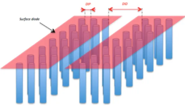
The main goal of this study is to demonstrate the functionality of 3D diodes as ESD discrete protection with significant silicon area reduction compared to classic 2D topology. The technology process is based on an existing one developed by IPDIA company [1][2] for the design of high-value capacitors. It is based on etching deep cylindrical micro-holes into the silicon and then filling them with polysilicon. In this particular case, the deposited polysilicon is highly doped with phosphorus. After a thermal diffusion, we obtain a three dimensional diode made up of an array of micro-holes connected in parallel. Back-to-back diodes are obtained by duplicating the resulting 3D diode as depicted in Fig 1.
Fig 1. Scheme of 3D back-to-back diodes.
The back-to-back configuration deviates the ESD current when the voltage at the protection electrode exceeds its breakdown voltage. A typical electrical implantation scheme as external protection is shown on Fig 2. The component is fully symmetrical i.e. the device protection is guaranteed for positive and negative ESD discharge. Clamping voltage requirement is tuned in the range of 10 to 80V regarding technological parameters. The array surface and the micro-hole density will define the current capability of the protection. In our case, the clamping voltage is fixed to 19V to fulfill a specific application requirement.
Fig 2. Typical implementation of external 3D back-to-back diode protection.
2. Layout parameter variations
In order to optimize ESD protection robustness we have studied two layout parameters (Figure1): the distance (DIP) between the micro-holes and the distance between the two 3D diodes (DID). As we decided to keep the same active area for each 3D diode, a smallest distance between holes allows increasing their density per diode (310 to 5700 units). A first study was carried out to determine the impact of this parameter on the breakdown voltage. The results of Figure 3 show that regardless of the number of micro-holes, the leakage current is very steady and the breakdown voltage is slightly the same (19V). The second parameter variation is the distance DID which was ranged between 35 to 165µm. We assumed that a trade-off has to be found between the current homogeneity during an ESD discharge and the silicon area impacted by a bigger distance between diodes.
Fig 3: DC curves for severals DIP lengths
Similarly, for all these devices there were no significant breakdown voltage variations with DID parameter.
2.1. DIP variation
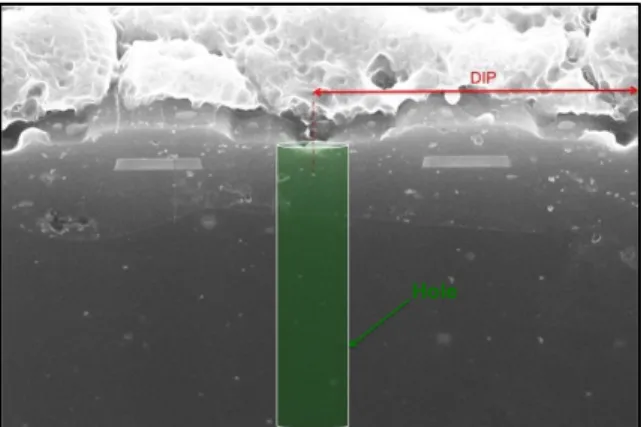
As the junction depth of the phosphorus-doped diffusion was unknown, we firstly determined the DIP distance resulting in the merging of the diffusions. Cross-sections of the devices were prepared using focus ion beam (FIB) and after a chemical revelation step, the phosphorus diffusion was highlighted.
Fig 4: Cross- section of a micro-hole showing the lateral phosphorus diffusion view for DIP=12um.
The cross-section of figure 4 shows the lateral diffusion for a large DIP distance of 12um, then. The DIP distance is sufficiently large to allow the formation of an individual junction around the micro-hole and then each hole can be considered as an elementary diode. A similarly study has been carried out when smaller DIP distances.
Fig 5: Cross section of holes with phosphorus diffusion view for DIP=4um.
Another cross-section on figure 5 has been processed with a DIP distance of 4um. We cannot observe the vertical junction anymore and it appears that all diffusions are merged. The distance allowing the merging of all diffusions and then the formation of a mega junction is approximately twice the width of a hole. In the next section, we studied the behavior of the device when DID distance is increased.
2.2. DID variation
TCAD simulations have been performed in DC analysis to extract the breakdown voltage, calibrate the simulator and study the impact of DID distance. As reported in Table 1, breakdown voltage is roughly the same whatever DID distance. The simulated value is slightly higher than the DC measurement. It can be explained by a slight mismatch on doping profile description. An ideal Gaussian profile is used for the simulations since we have not the actual lateral diffusion profile.
Table1: DC simulation for several DID values. DID (µm) 35 55 75 95 125 165
BV (V) 22.5 22.7 22.9 23 23.1 22.3
To understand the behavior of the previous device during an ESD event, a study has been carried out with T C A D simulation tools. Several assumptions were chosen for the simulator parameters. Thermal models have been neglected. In case of evaluating thermal breakdown this assumption should be critical but in our case, we want only
to highlight the difference in current distribution from a device to another. The purpose of the simulations is not to find the failure current, IT2. The benefit is to provide a good simulation convergence and avoid the limited thermal validity (600K-800K) of the impact ionization models [3].
Figure 6: Doping concentration distribution of studied device.
During experimental TLP measurement, t h e I-V curve is constructed by extracting, for a given pulse, the device current and voltage between 70 and 80 ns. We consider that during this time slot stationary regime is achieved. Based on this assumption high current simulations are performed using ACS (average current slope) technique [4]. A single current ramp (10A, 100ns) is applied to the device rather than using several TLP pulses. The numerical calculation exhibits a better convergence and a great computational time speed-up. The major drawback of this method is a possible overvoltage during device triggering that could not be detected [5] but this is not a critical issue in this device. The third assumption concerns the structure geometry. A complete structure description is very complex and would lead to a huge structure mesh. We chose to perform bi-dimensional simulation with a limited number of holes (10) for each diode, as shown on Figure 6. For the total current calculation, an area factor has been tuned to fit the real device configuration. ESD robustness is dependent on the DID distance between the two back-to-back diodes. In particular, we want to demonstrate that DID distance has an impact on the current distribution in the structure.
Figure 7: Current distribution at each anode (A1 to A10) for several DID lengths for a DIP distance of
?µm simulated with the structure of Figure 6. Figure 7 shows the different current distribution in each anode of the 10 individual diodes for DID ranging from 35um to 165um. Up to 20-28% of the current is supported by the first anode. For a higher DID distance, the current begins to increase progressively at the further extremity of the structure.
3. Results
The hypothesis on the current behavior in the structure must be verified. The following measurement data (Figure 8) show the advantage of the 3D technology compared to the 2D one for the same silicon area of 4032um2. Moreover, these results also demonstrate the impact of DID distance and its interest to improve ESD robustness.
Figure 8: IT2-VT2 curves for Planar2D, Well3D back-to-back diode and for several DID lengths
As confirmed by IT2-VT2 curves of figure 8, compared to 2D planar diode, using the silicon volume provides a strong advantage regarding ESD robustness. Performance in term of current capability is approximately twice better thus verifying our assumption of better current distribution. When DID distance is extended, the intrinsic resistance of the device increases too, which should degrade ESD robustness in terms of power dissipation. But, as this added resistance acts as a ballast resistance, the resulting on-resistance of the device during ESD, is lowered because current flow distribution is more homogeneous.
TLP curve (Fig 9.b) exhibits an amazing behavior. For a 10A TLP current (roughly 15 kV HBM stress), leakage current starts to progressively increase by step.
Fig 9: (a) top view of DUT (b) TLP curve (red) and leakage current (green). Circles indicate damaged
micro-holes.
A first micro-hole is damaged as indicated in Fig 9.a. But as the micro-holes are connected in parallel, this latter blows-up, and the rest of the structure is still functional with a reasonable leakage current always under 1µA which is our failure criteria. For multiple higher stresses other micro-holes are damaged but the device is still operating up to 16A TLP current. Depending on the application where this protection diode is integrated, it is considered definitely destroyed when the leakage current reaches 1µA. However, this partial destruction of the device might induce latent defects in the component to be protected. This behavior has been more deeply investigated by varying the width of structure. In this device, each micro-hole can be considered as an elementary diode. Then the robustness is limited by the number of damaged holes.
Fig 10: Top view of ESD protections with increasing area.
The structure width impact on the distribution of these damaged holes is shown in Fig 10. For small width (≤150µm), the on-resistance is high, and the current path is mainly focused on the first row of holes. IT2 is equal to 4.5A. However, when this parameter increases, the further holes appear to be more involved in the total current flow, then resulting in a better current homogeneity. Damaged holes are scattered and ESD robustness is improved, IT2 is 11.1A for the largest device (350µm) (see Figs. 11 and 12).
4. Device optimization
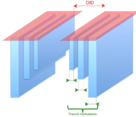
In the aim to enhance ESD robustness, we proposed a novel design of the device. The emerging idea consists of replacing the rows of micro-holes by trenches. The main advantage of trenches is that the etching process can benefit of more degrees of freedom. The trenches configuration has been optimized and finally a progressive modulation of both width and depth have been chosen.
Figure 11: Scheme of 3D back-to-back Trench diodes with width and depth modulation.
As the trench width impacts the trench depth during the etching process, the singularity of this new device is that the width and depth of trenches
increases from the front to the rear of the structure. TCAD simulations have demonstrated that this trench modulation decreases on-resistance and improves current homogeneity [6].
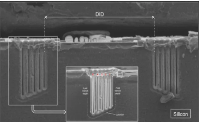
Figure 12: Cross-section of trench diode with 300nm step width.
With a width modulation of 300nm between trenches, the last trench is 5 µm deeper than the first one. This depth variation could be higher with a bigger difference between the width of the first and last trenches. But this technological parameter is not yet calibrated. . New trench back-to-back diodes
(Trench 3D) have been processed with a fixed silicon
area of 4032um2 and several DID values. Furthermore the width modulation between trenches was kept at 300 nm. TLP measurements have been performed and the failure current is reported in Figure 13 and compared to the previous 3D devices (Well 3D) having the same area and DID.
` Fig 13: Comparison of measured IT2-VT2 curves for Trench 3D back-to-back diode and previous 3D
diodes for several DID lengths
TLP results of figure 13 show that Trench 3D diodes
exhibit a very good ESD performance. IT2 value is roughly doubled compared to initial 3D devices (Well 3D). Meanwhile VT2 value is almost the same. This clearly demonstrates that the on-resistance during ESD stress is reduced. The configuration of full-length trenches mixed together with the modulation of their width greatly improve the current distribution into the device. The main reason for performance improvement results in the current path in this structure. In fact, with this variation of width and depth, we promote current conductivity at the depth of these trenches. However, the progressive modulation of width allows decreasing resistance and showing a better current homogeneously at the rear of the diode.
Fig 14: TLP curve (red) and leakage current (green) showing spontaneous failure of device
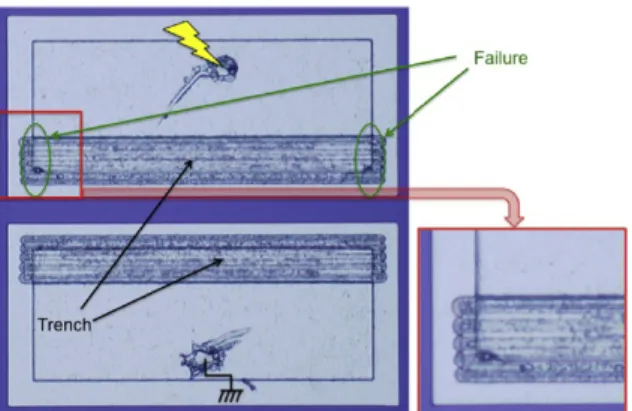
TLP measurement data of figure 14 show that the leakage current, measured after each increasing TLP stress, exhibits a different behavior compared to the previous 3D diodes. In this case the leakage current present an abrupt increase, higher than the 1uA failure criteria, when IT2 is reached. The failure mechanism is different because a trench is more robust than several holes in parallel. Figure 15 shows a picture of the device after a 18kV HBM stress which lead to a failure. Two failure points are located in the metal corner of the reverse biased diode. Given this result, another potential way to improve ESD robustness is related to the optimization of the metal layout.
Figure 14: (a) View of ESD failure after 18kV HBM
stress. (b) Zoomed-in-view of the failure spot at the guard ring corner.
5. Conclusion
This work presents a novel 3D back-to-back diode ESD discrete protection based on a technology process dedicated to manufacturing high-value 3D capacitors. The etch step, necessary to form the capacitor, is used to produce three-dimensional elementary diodes. These elements are combined to form back-to-back 3D diodes without additional technological step. This structure is appropriate to external, first stage, protection for high voltage ICs. Combining i n the same component, high capacitors for filtering or decoupling, and efficient ESD protection, is a great challenge in system-level consideration. This study is based on experimental measurement on several test vehicles but also on TCAD simulations to better understand the device behavior in high current regime. The impact of layout variations on ESD robustness is also studied. Two original structures are proposed: the first 3D diode directly uses the structure of the 3D capacitors that is made up of an array of micro-holes in parallel and the second one uses rows of modulated trenches (Trench 3D diode).
First, TLP measurement results showed that the first 3D diode exhibits an ESD robustness that is twice the one of a Planar2D device for the same silicon area (about 4032 µm2 for a single diode and 30 000 µm2 for the full device).. However, the failure mechanism of this 3D diode is characterized by a progressive leakage current increase by step, each step corresponding to the blow-up of a micro-hole. Secondly, for the same silicon area, the Trench 3D device provides 22.7kV HBM robustness against
only 13.6kV for initial 3D device corresponding to an increase about 50%. In addition, the failure mechanism exhibits an abrupt increase of leakage current that is preferable for long-term reliability. Failure location is within the metal that allows expecting even more ESD robustness by optimizing its layout.
References
[1] F. Murray, “Silicon based system-in-package: a passive integration technology combined with advanced packaging and system based design tools to allow a breakthrough in miniaturization”, IEEE-BCTM, pp. 169-173, 2005. [2] S. Gaborieau, C. Bunel, F. Murray, “3D Passive Integrated Capacitors Towards Even Higher Integration”, IMAPS 2010.
[3] C. Salamero, N. Nolhier, M. Bafleur and P. Besse, "Accurate prediction of the ESD robustness of semiconductor devices through physical simulation", IEEE-IRPS, pp 115-8, 2005.
[4] Galy et al. “Numerical evaluation between Transmission Line Pulse (TLP) and Average Current Slope (ACS) of a submicron gg-NMOS transistor under Electro-Static Discharge (ESD)”, Workshop EOS/ESD/EMIp. 15– 22, 2002.
[5] A. Delmas, A. Gendron, M. Bafleur, N. Nolhier and C. Gill, "Transient voltage overshoots of high voltage ESD protections based on bipolar transistors in smart power technology", IEEE-BCTM, pp253-256, 2010.
[6] B.Courivaud, N.Nolhier, G.Ferru, M.Bafleur and F.Caignet, "Novel 3D back--‐to--‐back diode ESD protection”, EOS/ESD Symposium, 2014.