HAL Id: hal-00802733
https://hal.archives-ouvertes.fr/hal-00802733
Submitted on 21 Mar 2013
HAL is a multi-disciplinary open access archive for the deposit and dissemination of sci-entific research documents, whether they are pub-lished or not. The documents may come from teaching and research institutions in France or abroad, or from public or private research centers.
L’archive ouverte pluridisciplinaire HAL, est destinée au dépôt et à la diffusion de documents scientifiques de niveau recherche, publiés ou non, émanant des établissements d’enseignement et de recherche français ou étrangers, des laboratoires publics ou privés.
nanowires on O-polar ZnO and on sapphire
Guillaume Perillat-Merceroz, Robin Thierry, Pierre-Henri Jouneau, Pierre
Ferret, Guy Feuillet
To cite this version:
Guillaume Perillat-Merceroz, Robin Thierry, Pierre-Henri Jouneau, Pierre Ferret, Guy Feuillet. Com-pared growth mechanisms of Zn-polar ZnO nanowires on O-polar ZnO and on sapphire. Nanotechnol-ogy, Institute of Physics, 2012, 23 (12), pp.125702. �10.1088/0957-4484/23/12/125702�. �hal-00802733�
generators, or light-emitting diodes. In this view, we investigate the nucleation and growth mechanisms of ZnO nanowires grown by metalorganic vapor phase epitaxy either on O-polar ZnO or on sapphire substrates. Whatever the substrate, ZnO nanowires are Zn-polar, as demonstrated by convergent beam electron diffraction. For growth on O-polar ZnO substrate, the nanowires are found to sit on O-polar pyramids. As growth proceeds, the inversion domain boundary moves up in order to remain at the top of the O-polar pyramids. For growth on sapphire substrates, the nanowires may also originate from the sapphire / ZnO interface. The presence of atomic steps and the non-polar character of sapphire could be the cause of the Zn-polar crystal nucleation on sapphire, whereas it is proposed that the segregation of aluminum impurities could account for the nucleation of inverted domains for growth on O-polar ZnO.
1. Introduction
ZnO nanowires are easily grown, with no catalysts, by different growth methods on various types of substrates such as sapphire [1], ZnO [2], GaN [3], silicon [4], metal [5], graphene [6], and glass [4]. Consequently, they are considered for many applications. For example, nanostructures with a high surface to volume ratio can be deposited onto low cost substrates, through cheap growth methods such as chemical bath deposition: when covered with a thin photon absorber, these nanostructures open the way to photovoltaic applications [7, 8]. Type II hetero-structures based on ZnO nanowires are
also envisaged to absorb the photons and separate the electron-hole pairs [9]. Another possible application field is the fabrication of nano-generators using the piezoelectric effect of ZnO nanowires in order to convert mechanical energy into electrical energy [10]. ZnO nanowires are also studied for applications in light-emitting diodes (LEDs) or lasers, but it is difficult to dope ZnO p-type. However, recent publications are encouraging concerning the feasibility of p-type doping [11, 12, 13]. Concerning nanowire LEDs, a weak ultra-violet emission was observed under current injection for p-n homo-junctions in ZnO nanowires [14, 15]. A more intense electroluminescence was obtained from hetero-junctions made of n-type ZnO nanowires coated with another p-type material, for example p-type GaN [16] or polymers [17]. Finally, an electrically-pumped laser made of Sb-doped p-type ZnO nanowires on a n-type ZnO thin film was demonstrated [18]. Using ZnO nanowires instead of two-dimensional ZnO layers presents definite advantages for engineering LEDs. Indeed, nanowire growth on large and conductive hetero-substrates such as silicon and metallic substrates is possible, and no structural defects are expected (as observed for nanowire growth on sapphire, where no structural defects were observed [19, 20]). Furthermore, core-shell quantum wells with a large developed surface, can be grown [21, 22, 23]. Finally, light extraction is naturally more efficient in a nanowire-based LED [24].
In order to reach these application goals, a controlled growth of the nanowires is necessary. For a large variety of materials such as GaN [25, 26, 27, 28, 29], GaAs [30], or InAs [31], the crystal polarity has a crucial role in both the nucleation and the growth of nanowires. Concerning ZnO, the role of crystal polarity was demonstrated already in 1972 by chemical etching for ZnO microwires grown by chemical vapor deposition (CVD): the microwires were oriented in the +c direction of the wurtzite structure (i.e. the Zn-polar [0001] direction)[32, 33]. The Zn-polarity of ZnO nanoribbons was confirmed by convergent beam electron diffraction (CBED) in 2003 [34]. A Zn-polarity was also observed for nanowires grown by the hydrothermal method [35], by catalyst-assisted CVD [36], by pulsed laser deposition (PLD) [37], and by evaporation of zinc in an oxygen plasma [38], with the CBED technique. Other methods such piezoelectric force microscopy have shown the Zn-polarity of nanowires grown by the hydrothermal method [39]. Consequently, it was deduced that the ZnO nanowire growth is due to a much higher growth rate along the + c direction. Results published about two-dimensional thin layers agree with those about nanowires, with a higher growth rate along the + c direction than along the - c direction (the O-polar [000¯1] direction) [40].
first publication by G.C. Yi’s group [1]. In these publications, nanowires are obtained on a spontaneously deposited ZnO under-layer, and sometimes the nanowires sit on top of ZnO pyramids. The influence of stress is invoked in some publications to explain the nanowire nucleation, because their larger surface-to-volume ratio would help release the misfit strain between sapphire and ZnO [44, 45, 48, 49]. But this mechanism cannot account for the homo-epitaxial growth of ZnO nanowires on ZnO substrates. In the case of MOVPE growth, the role of the crystal polarity in the growth and nucleation mechanisms of ZnO nanowires, although mentioned in Ref.[20], has not been discussed thoroughly.
In this work, we aim to elucidate the role that polarity plays in defining the morphology of MOVPE grown nanostructures. A comparison is carried out on three different substrates: sapphire, O-polar ZnO, and O-polar thick ZnO buffer layer grown previously on sapphire. For the growth on sapphire, the normally reported morphology with an unintentional under-layer, pyramids and nanowires is observed. For the direct growth on O-polar ZnO (either on intentional buffer layers or on bulk substrates), pyramids and nanowires are also observed. In every case, the crystal polarity is determined by CBED, allowing us to link the shape of the nanostructures with their polarity: whatever the substrate, nanowires are found to be Zn-polar whereas the under-layers and the pyramids are O-polar. Inversion domain boundaries (IDBs) are observed by transmission electron microscopy (TEM), providing important indications on the nucleation mechanisms. Observations of numerous nanowires for each kind of sample allowed us to draw a clear picture of the nucleation mechanisms involved for the different substrates used. On sapphire, it is proposed that the non-polar character and the atomic steps of this substrate are the cause for the germination of Zn-polar nanowires. For the nucleation of Zn-polar ZnO on O-polar ZnO, the role of aluminum impurities is
discussed.
2. Experimental details
Three types of ZnO nanowire samples have been studied. Growth was carried out either directly on (0001) sapphire substrates, or on a 400 nm thick buffer layer previously deposited on (0001) sapphire substrates, or on O-polar hydrothermally-grown bulk ZnO substrates (provided by Crystec). N2 was used as the carrier gas, N2O as the oxygen
precursor and diethylzinc as the zinc precursor. The pressure in the reactor was around 100 mbar. The molar ratio between the O precursor and the Zn precursor allowed controlling the morphology of the deposition: this ratio was about 500 for nanowire growth, and about 25000 for the two-dimensional buffer layer growth. The growth temperature was between 750 and 850°C for the nanowires, and of 950°C for the buffer layer. A reactor without any rotating stage was used. Consequently, there is a slight variation of the nanowire sizes from the center to the edge of the substrate.
Cross-sectional TEM samples were prepared either by the cleaved edge method [50], or by mechanical polishing followed by ion milling. The two-beam technique with g = (0002)diffracting conditions was used to delineate domains with different polarities. Convergent beam electron diffraction (CBED) patterns acquired along a h1¯100i zone axis were used to determine the crystal polarity. To determine the orientation of the CBED patterns relatively to the image, the sample is mechanically lowered from the focal point in order to obtain a shadow image in the diffraction disk without 180° rotation. Simulations performed with the JEMS software [51] were used in order to index the (0002)and the (000¯2) directions on the CBED experimental patterns, and consequently to deduce the nanostructure polarities. Scanning TEM (STEM) images were acquired with a high-angle annular dark field detector to localize the position of the beam used for CBED. High-resolution TEM images were acquired along h11¯20i zone axis.
3. Results
3.1. Morphology of the nanostructures
The nanowire morphology for the growth on sapphire was described in two previous papers [19, 20]. We recall here the main results. Figure 1 presents scanning electron microscopy (SEM) images of vertical nanowires grown on sapphire for a 45 min
Figure 1. SEM images of ZnO nanowires and pyramids, grown during 45 min on (0001) sapphire: (a) tilted view, (b) top view.
deposition time. They all present a pyramidal base, even if some pyramids have no nanowire at their top. From x-ray diffraction rocking-curves, the (002) ZnO planes and the (006) sapphire planes were found to be parallel, showing that the ZnO nanowires grew along the c direction [19]. On the top-view SEM image (figure 1 (b)), it is seen that the nanowires have a hexagonal section, and that they all exhibit the same in-plane orientation with respect to sapphire. Two in-plane orientation relationships are usually found for ZnO grown on (0001) sapphire: in-plane rotations of 0° or 30° can be observed [52]. Here, only the 30° rotation is observed, that is to say the orientation relationship is [0001]ZnO//[0001]sapphire, and h1¯100iZnO //h11¯20isapphire [20]. The nanowires exhibit
{¯1100} lateral faces, and do not contain any structural defects such as dislocations or stacking faults [20].
As it was observed in all publications about growth of ZnO nanowires on sapphire, a ZnO wetting layer is unintentionally formed [1, 42, 43, 44, 46, 47, 19, 20]. It is present at the very beginning of the growth, even after a one minute growth it is visible on the high resolution TEM image in figure 2.
Figure 3 presents scanning electron microscopy (SEM) images of vertical nanowires grown on a ZnO buffer layer deposited on (0001) sapphire (Figure 3 (a)), and on a (000¯1)
Figure 2. High resolution TEM image of a ZnO pyramid (without any nanowire) on the ZnO wetting layer, on the sapphire substrate, after one minute growth.
Figure 3. SEM images of ZnO nanowires and pyramids, grown during (a) 45 min on a ZnO buffer layer on (0001) sapphire, and (b) during 25 min on (000¯1) ZnO.
ZnO substrate (Figure 3 (b)). As for the growth on sapphire, all nanowires present a pyramidal base.
3.2. Polarity determination
The polarity of ZnO nanowires and pyramids was determined for two types of samples, one grown on a ZnO buffer layer, and the other grown directly on sapphire. Figure 4 (a) is a STEM image of a nanowire on top of a pyramid, on the 400 nm thick ZnO buffer layer previously deposited on sapphire. The CBED patterns corresponding to the nanowire are shown in figure 4 (b) with the experimental pattern on top, and the simulated one at the bottom. The growth direction is along the [0002] direction: in other words, the nanowire is Zn-polar. The CBED experimental and simulated patterns (top and bottom respectively) corresponding to the pyramid are shown in figure 4 (c). The growth direction is along the [000¯2] direction: pyramids are O-polar. Similarly, the CBED patterns of figure 4 (d) reveals the O polarity of the ZnO buffer layer. Thus, we might infer that opposite crystal polarities lead to very different growth rates:
Figure 4. (a) STEM image of a ZnO nanowire on top of a ZnO pyramid on a ZnO buffer layer, on the sapphire substrate. (b)(c)(d) Experimental (top) and simulated (bottom) CBED patterns of the nanowire, the pyramid, and the buffer layer, respectively. Simulation for ZnO thicknesses of 46, 110, and 140 nm respectively, done with the JEMS software [51]. For all CBED patterns, the growth direction is upwards. The nanowire is Zn-polar, the pyramid and the buffer layer are O-polar.
Zn-polar crystals lead to nanowires while O-polar crystals lead to pyramids, for the conditions used here for nanowire growth. Ab-initio calculations help to explain this strong anisotropy, which is observed whatever the elaboration method is. The cohesion energies of Zn and O atoms on the two {0001} surfaces were calculated [53]. For a Zn-O dimer, they are similar for the two surfaces. However, the zinc cohesion energy is much more important on the (0001) Zn-polar surface (-6.9 eV) compared to the (000¯1) O-polar surface (-1.3 eV): this could explain the strong growth anisotropy along the ± c directions.
CBED experiments were also done for nanowires and pyramids grown directly on sapphire, with the presence of an unintentional ZnO wetting layer (figure 5). Once again, nanowires are Zn-polar and the pyramids are O-polar. It was not possible to determine the polarity of the thin wetting layer, maybe because of the presence of numerous structural defects. However, the same morphology with pyramids and nanowires is obtained on this thin wetting layer, and on the O-polar buffer layer and on O-polar hydrothermal substrates. This is in contrast with the growth on Zn-polar substrates, for which only a thin two-dimensional layer was obtained instead of nanowires for the same growth conditions (result not shown here). Consequently we assume that this wetting layer is also O-polar. This dependence of the nanostructure shape on the crystal polarity seems to be general for wurtzite materials. For example, it was shown for MOVPE-grown GaN nanostructures that pyramids were Ga-polar and nanowires N-polar [25, 26, 27].
Figure 5. (a) STEM image of a ZnO nanowire and a ZnO pyramid on a unintentional ZnO wetting layer on sapphire. Experimental (up) and simulated (down) CBED patterns (b) of the nanowire, and (c) of the pyramid, with the growth direction upwards. Simulations with the JEMS software for thicknesses of 100 and 113 nm [51].
Figure 6. Two-beam TEM image with g = (0002) of a Zn-polar nanowire on a O-polar pyramid, grown during 45 min on a ZnO buffer layer on sapphire. The IDB between the nanowire and the pyramid is at the top of the pyramid, as observed in 90% of cases for the growth on O-polar ZnO.
3.3. Inversion domain boundaries : position and formation
After having determined that pyramids were O-polar and nanowires were Zn-polar, the position and shape of the interface between these inverted domains has been studied by two-beam TEM. The results for the growth on O-polar substrates or on O-polar buffer layer are reported in this section, and those concerning the growth directly on sapphire in the following one.
Figure 6 shows a g = (0002) TEM image of a nanowire on a pyramid, grown on an O-polar ZnO buffer layer on sapphire. Clearly, the Zn-polar domain begins at the top of the O-polar pyramid. The same result was obtained for all of the ten nanowires and
Figure 7. Two-beam TEM images with g = (0002) of a Zn-polar nanowire and a O-polar pyramid grown on an O-polar ZnO substrate. The Zn-polar domain of the nanowire continues under the top of the pyramid, which is observed in 10% of cases for the growth on O-polar ZnO.
Substrate Deposition IDB at the top IDB inside IDB at the interface time of the pyramid the pyramid with the substrate Sapphire + buffer ZnO 45 min 10/10 0/10 0/10
ZnO 5 min 7/7 0/7 0/7
ZnO 5 min 17/22 5/22 0/22
ZnO 25 min 11/11 0/11 0/11
Sapphire 30 min 8/18 2/18 8/18
Table 1. Summary table of the position of the IDBs according to the samples.
pyramids observed on this sample. These observations were repeated for nanowires and pyramids grown during five minutes on a O-polar ZnO substrate. For all of the seven observations, the IDBs are also found to be lying at the top of the pyramid. Two other samples were grown on ZnO substrates with exactly the same growth conditions, but with different deposition times of 5 and 25 min. On the 25 min sample, the IDBs were found at the top of the pyramids for all of the 11 observations. This is in contrast with the sample grown for 5 min, where, for 5 nanowires over 22, the Zn-polar domain seems to originate from a certain depth within the pyramids but never from the interface with the substrate (figure 7). For the 17 other wires, the IDBs lie at the top of the pyramid as usually observed. The statistics of these observations are summarized in table 1. Considering the four samples grown on O-polar ZnO (one growth on a buffer layer, and
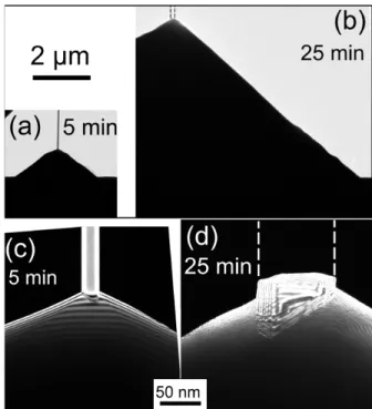
Figure 8. Two-beam TEM images with g = (0002) of Zn-polar nanowires on top of O-polar pyramids, grown on an O-polar ZnO substrate, for (a) (c) 5 min of growth and (b) (d) 25 min of growth. (a) (b): low magnification images at the same scale. (c) (d): zooms on the IDBs at the tops of the pyramids. The dashed lines on images (b) and (d) recall the position of the nanowire removed during the TEM sample preparation.
the three other growths on bulk substrates), it is deduced that in 90% of cases, the Zn-polar domain sits at the top of the O-polar pyramid. It is interesting to notice that the IDBs present inclined facets rather than basal ones: this point will be discussed later.
Figure 8 images a nanowire on top of a pyramid after a 5 min growth ((a) and (c)), and after a 25 min growth ((b) and (d)). Figure 8 (a) and (b) are low magnification images of ZnO pyramids at the same scale: pyramids have grown in height and diameter with time. Similarly, nanowires have grown, even if the variation in height is not visible on these images. By observations of many pyramids and nanowires (22 observations for 5 min growth and 11 observations for 25 min growth), we determined that the pyramid heights after 5 min growth are between 0.5 and 1.3 µm, with a mean height of 0.8 µm. Nanowire diameters are between 10 and 100 nm, with an average value of 50 nm. For a 25 min growth, the pyramid heights are between 1 and 9 µm, with an average height of 5 µm. Nanowire diameters are between 20 and 300 nm, with an average diameter of 180 nm. Consequently, the pyramids and nanowires presented in figure 8 (a) and (b) are thought to be representative. The IDB is at the top of the pyramid for the 5 min
Figure 9. (a) Scheme of a Zn-polar nanowire growth on top of a O-polar pyramid. (b) The Zn-polar domain moves up during the growth and stays at the top of the pyramid. (c) The Zn-polar domain does not move during growth.
growth (figure 8 (c)), and it stays at the top of the pyramid after 25 min of growth (figure 8 (d)). It is deduced that the IDB moves up during the growth of the pyramid and of the nanowire.
Figure 9 is a schematic of this IDB movement. On figure 9 (a), the Zn-polar nanowire is drawn on top of the O-polar pyramid. Figures 9 (b) and (c) present the nanowire and the pyramid later during the growth, in the case where the IDB moves up (figure 9 (b)), and in the case where the IDB does not move. In this latter case vertical IDBs (in red on figure 9 (c)) are formed. We assume that in the general case (90% of cases), the energy necessary to move the IDB is smaller than the formation energy of the vertical IDB on the side walls of the nanowires. Consequently, the upward movement of the IDB would be favored. There is no data in the literature about the ZnO IDB energies. One possibility would be to determine the atomic structure of the inclined and vertical IDBs from high-resolution TEM images, and then calculate the IDB energies by ab-initio calculations. But the sample preparation to obtain a nanowire on a pyramid with a thickness less than 50 nm is very tricky. We will discuss in subsection 4 on the possible influence that segregating aluminum impurities coming from the sapphire substrate or from the ZnO substrate could bear on the formation of the IDBs. The displacement rate of the IDBs might be correlated with the diffusion rate of Al, because impurities may have a drag effect during grain boundary movement [54]. Different impurity concentrations may explain the fact that in 10% of the cases (for the growth on O-polar ZnO), the IDB is pinned inside the pyramid. Moreover, the grain boundary movement is thermally activated because it is linked to the diffusion of Zn and O atoms
Figure 10. Two-beam TEM images with g = (0002) of ZnO pyramids and nanowires grown during 30 min directly on sapphire : (a) IDB at the top of the pyramid, (b) IDB inside the pyramid, (c) IDB originating from the sapphire / ZnO interface. The dashed lines recall the position of the nanowires broken during the TEM sample preparation.
and of extrinsic impurities. Thus studying the influence of the temperature and of growth durations on the movement of the IDBs could yield valuable informations on the activation energy for this movement. However, the variation range of temperature is limited, because the nanostructure morphology is temperature-dependent.
For comparison, IDBs are examined for growth directly on sapphire. The presence of an unintentional ZnO wetting layer, together with pyramids and nanowires has been noticed earlier. Figure 10 shows TEM images with g = (0002) for three different
4. Discussion: nanowire nucleation 4.1. Nanowire nucleation on O-polar ZnO
The spontaneous nucleation of Zn-polar nanowires on O-polar ZnO has never been reported in the literature. It is interesting to compare with the GaN case, which has the same wurtzite structure as ZnO. In this discussion, the literature concerning GaN is briefly reviewed, then the role of impurities related to the polarity inversions in ZnO is examined.
For GaN, spontaneous polarity inversions during growth have never been observed. However, doping with Mg is often correlated with the formation of polarity inversion domains during the growth of thin two-dimensional layers [55, 56, 57]. For MOVPE growth, small triangular domains with an inverted polarity compared to the matrix are observed because of Mg-doping. In these samples, the average Mg concentration is estimated to be 1019cm-3. The shape of the triangular domains is shown in figure 11
(a) for a matrix growing in the + c direction (Ga polarity), and in figure 11 (b) for a matrix growing in the - c direction (N polarity). Inclined IDBs are observed for the so-called head-to-head configuration, whereas basal IDBs are observed for the tail-to-tail configuration [56]. Concerning GaN nanostructures grown by MOVPE, nanowires are N-polar and pyramids Ga-polar. However, nucleation of N-polar nanowires occurred either directly on sapphire, or on N-polar GaN covered by a thin SiNx mask, but never
on Ga-polar pyramids [25].
Concerning two-dimensionnal ZnO layers, it was observed that their polarity depended on Al doping. For ZnO growths without doping on sapphire [59] or on glass [60], O-polar ZnO was obtained. However, when ZnO was doped with 1% Al, a Zn-polar layer is obtained. For application in varistors, polycrystalline ZnO is synthesized
Figure 11. Configuration of the inverted domains for (a), (b) Mg-doped GaN [56], and (c) Fe2O3-doped ZnO [58]. Arrows indicate the +c direction. (a) N-polar domain
in a Ga-polar matrix (b) Ga-polar domain in a N-polar matrix. (a) and (b): for GaN, configuration head-to-head for the inclined IDBs, and tail-to-tail for the basal IDBs. (c) For ZnO, configuration tail-to-tail for the inclined IDBs, and head-to-head for the basal IDBs.
by sintering of ZnO powders with the addition of others oxides such as SnO2 [61] or
Fe2O3 [58]. These dopants are known to form spinel phases with ZnO and to trigger
the formation of IDBs in the ZnO crystals. It is deduced that for doped ZnO, a microstructure with IDBs is thermodynamically more stable than a solid solution of dopants in ZnO. Models are proposed for the formation of basal plane IDBs [61], and inclined plane IDBs [58]. According to these works, dopants can diffuse into ZnO, and segregate to octahedral sites of the ZnO hexagonal structure. To preserve the local charge balance, Zn atoms are displaced to form inverted domains. IDBs with basal planes are created in the case of impurities with an oxidation state greater than three such as Sn, while IDBs with basal and inclined planes are created in the case of impurities with an oxidation state equal to three such as Fe.
For Fe-doped ZnO, the shape of the IDBs is shown in figure 11 (c): IDBs lie in the basal planes for a head-to-head configuration, and in inclined planes for a
tail-Al was not detected on the IDBs by electron dispersive x-ray spectroscopy (EDX), probably because the concentration is too low.
In order to prove the role of Al in the nucleation of polarity inversion, it would be interesting to grow nanowires and pyramids simultaneously on purer ZnO substrates (for example, those provided by Tokyo Denpa with an Al concentration of about 5.1015
cm-3), on the ZnO substrate used here (provided by Crystec with an Al concentration of
about 5.1017 cm-3), and on an intentionally doped ZnO layer (with an Al concentration
of about 1019cm-3). For a higher aluminum doping, we would expect a higher nanowire
density, and Al might be detected by EDX (or another method) on the IDBs.
4.2. ZnO nanowire nucleation on sapphire
Contrary to the nucleation of ZnO nanowires on ZnO substrates, direct nucleation on sapphire is well documented. Three hypothesis are commonly proposed in the literature, and discussed below. A majority of publications describing the MOVPE growth of ZnO nanowires on sapphire invokes the role of stress to explain the nucleation [44, 45, 48, 49]. Nanowires would help to release the stress in the ZnO under-layer thanks to their free surfaces. This mechanism may be valid, but it is uncomplete because it does not take into account the fact that the under-layer and the nanowires have different polarities. Furthermore, as discussed previously, nanowires are found to nucleate as well on ZnO substrates: the stress hypothesis can be ruled out in this case. Finally, it does not explain the nucleation at the sapphire ZnO interface.
The role of atomic steps in the nucleation of IDBs was proposed first for GaN [64]. The nucleation of an IDB above an atomic step helps accommodating the misfit due to the vertical translation of the two crystals on each side of the atomic step. For ZnO, IDBs nucleating at atomic steps were also observed [46]. In our case, we rarely
observed an alignment of the nanowires along the sapphire crystallographic directions [20]. Consequently, we think that atomic steps are only one possibility to initiate polarity inversions with the subsequent formation of nanowires.
Another possibility for the nanowire nucleation is proposed by Cherns et al [37]. Based on their TEM observations, they proposed that the Zn-polar domains which give rise to nanowires during the PLD growth on sapphire directly originated from the sapphire surface. This would be due to the initial growth conditions. They recall that ZnO of both polarities can be obtained in a controlled manner depending on the sapphire surface treatments [65, 66]. Moreover, polarity inversions originating at the ZnO / sapphire interface were observed during the growth of thin layers [67] on sapphire. Actually, because sapphire is non polar, it is not surprising that both polarities can be obtained. In our case, the wetting layer of O-polarity would result from the lateral growth of the O-polar nuclei, with a few Zn-polar nuclei inclusions. These Zn-polar nuclei would give rise to Zn-polar nanowires because of the strong anisotropy between the growth rates of O-polar and Zn-polar ZnO.
5. Summary
The nucleation mechanisms of ZnO nanowires were investigated for different types of substrates, namely c-oriented sapphire and O-polar ZnO. The MOVPE-grown nanostructures mainly consist of pyramids with nanowires sitting on top. It was shown by CBED that, whatever the substrate, nanowires and pyramids have opposite polarities: nanowires are Zn-polar and pyramids are O-polar. The examination of the inversion domain boundaries (IDBs) for a fair population of nanowires grown either in homo-epitaxy on O-polar ZnO templates or substrates, or in hetero-epitaxy on sapphire, allowed us to draw a clear picture of the nucleation mechanisms at play in the two cases. For growth on O-polar ZnO, nanowire nucleation implies the creation of an inverted domain. Its origin is discussed and possibly attributed to the presence of aluminum impurities diffusing from the substrates. This hypothesis would need to be comforted by comparing nanowires grown on ZnO substrates with different residual aluminum concentrations and on aluminum doped ZnO templates. The IDBs formed between the O-polar pyramid and the Zn-polar nanowire was shown to move during the growth, and to be always located at the top of the pyramid. For growth on sapphire substrates, the nucleation of Zn-polar domains occurred either on the O-polar pyramids, or directly on
The authors acknowledge funding from the French national research agency (ANR) through the Carnot program (2006/2010).
References
[1] W. I. Park, D. H. Kim, S.-W. Jung, and Gyu-Chul Yi. Metalorganic vapor-phase epitaxial growth of vertically well-aligned ZnO nanorods. Applied Physics Letters, 80(22):4232–4234, June 2002. [2] C. Thiandoume, J. Barjon, O. Ka, A. Lusson, P. Galtier, and V. Sallet. Morphology transition of one-dimensional ZnO grown by metal organic vapour phase epitaxy on (0 0 0 1)-ZnO substrate. Journal of Crystal Growth, 311(18):4311–4316, September 2009.
[3] Y. J. Hong, S. J. An, H. S. Jung, C.-H. Lee, and G.-C. Yi. Position-Controlled selective growth of ZnO nanorods on si substrates using Facet-Controlled GaN micropatterns. Advanced Materials, 19(24):4416–4419, 2007.
[4] Dong Ju Lee, Jae Young Park, Young Su Yun, Yong Sung Hong, Jong Ha Moon, Byung-Teak Lee, and Sang Sub Kim. Comparative studies on the growth behavior of ZnO nanorods by metalorganic chemical vapor deposition depending on the type of substrates. Journal of Crystal Growth, 276(3-4):458–464, April 2005.
[5] SS Park, JM Lee, SJ Kim, SW Kim, HH Lee, SH Kim, and S Fujita. Catalyst-free synthesis of ZnO nanorods on metal substrates by using thermal chemical vapor deposition. Journal of the Korean Physical Society, 53(1):183–187, July 2008.
[6] Yong-Jin Kim, Jae-Hyun Lee, and Gyu-Chul Yi. Vertically aligned ZnO nanostructures grown on graphene layers. Applied Physics Letters, 95(21):213101–3, November 2009.
[7] Seung Hwan Ko, Daeho Lee, Hyun Wook Kang, Koo Hyun Nam, Joon Yeob Yeo, Suk Joon Hong, Costas P. Grigoropoulos, and Hyung Jin Sung. Nanoforest of hydrothermally grown hierarchical ZnO nanowires for a high efficiency Dye-Sensitized solar cell. Nano Letters, 11(2):666–671, February 2011.
[8] V. Consonni, G. Rey, J. Bonaime, N. Karst, B. Doisneau, H. Roussel, S. Renet, and D. Bellet. Synthesis and physical properties of ZnO/CdTe core shell nanowires grown by low-cost deposition methods. Applied Physics Letters, 98(11):111906, 2011.
[9] Zhiming Wu, Yong Zhang, Jinjian Zheng, Xiangan Lin, Xiaohang Chen, Binwang Huang, Huiqiong Wang, Kai Huang, Shuping Li, and Junyong Kang. An all-inorganic type-II heterojunction array
with nearly full solar spectral response based on ZnO/ZnSe core/shell nanowires. Journal of Materials Chemistry, 21(16):6020, 2011.
[10] Sheng Xu, Yong Qin, Chen Xu, Yaguang Wei, Rusen Yang, and Zhong Lin Wang. Self-powered nanowire devices. Nature Nanotechnology, 5(5):366–373, May 2010.
[11] K. Nakahara, S. Akasaka, H. Yuji, K. Tamura, T. Fujii, Y. Nishimoto, D. Takamizu, A. Sasaki, T. Tanabe, H. Takasu, H. Amaike, T. Onuma, S. F. Chichibu, A. Tsukazaki, A. Ohtomo, and M. Kawasaki. Nitrogen doped MgZnO/ZnO single heterostructure ultraviolet light-emitting diodes on ZnO substrates. Applied Physics Letters, 97(1):013501, 2010.
[12] S. Lautenschlaeger, M. Hofmann, S. Eisermann, G. Haas, M. Pinnisch, A. Laufer, and B. K Meyer. A model for acceptor doping in ZnO based on nitrogen pair formation. physica status solidi (b), 248(5):1217–1221, May 2011.
[13] H. Kato, T. Yamamuro, A. Ogawa, C. Kyotani, and M. Sano. Impact of mixture gas plasma of n2 and o2 as the n source on ZnO-Based ultraviolet Light-Emitting diodes fabricated by molecular beam epitaxy. Applied Physics Express, 4:091105, 2011.
[14] M Willander, O Nur, QX Zhao, LL Yang, M Lorenz, BQ Cao, JZ Perez, C Czekalla, G Zimmermann, M Grundmann, A Bakin, A Behrends, M Al-Suleiman, A El-Shaer, AC Mofor, B Postels, A Waag, N Boukos, A Travlos, HS Kwack, J Guinard, and DL Dang. Zinc oxide nanorod based photonic devices: recent progress in growth, light emitting diodes and lasers. Nanotechnology, 20(33):332001, August 2009.
[15] Min-Teng Chen, Ming-Pei Lu, Yi-Jen Wu, Jinhui Song, Chung-Yang Lee, Ming-Yen Lu, Yu-Cheng Chang, Li-Jen Chou, Zhong Lin Wang, and Lih-Juann Chen. Near UV LEDs made with in situ doped p-n homojunction ZnO nanowire arrays. Nano Letters, 10(11):4387–4393, November 2010.
[16] Oleg Lupan, Thierry Pauporte, and Bruno Viana. Low-Voltage UV-Electroluminescence from ZnO-Nanowire Array/p-GaN Light-Emitting diodes. Advanced Materials, 22(30):3298–3302, August 2010.
[17] M Willander, O Nur, N Bano, and K Sultana. Zinc oxide nanorod-based heterostructures on solid and soft substrates for white-light-emitting diode applications. New Journal of Physics, 11(12):125020, December 2009.
[18] Sheng Chu, Guoping Wang, Weihang Zhou, Yuqing Lin, Leonid Chernyak, Jianze Zhao, Jieying Kong, Lin Li, Jingjian Ren, and Jianlin Liu. Electrically pumped waveguide lasing from ZnO nanowires. Nature Nanotechnology, 6(8):506–510, 2011.
[19] M. Rosina, P. Ferret, P.-H. Jouneau, I.-C. Robin, F. Levy, G. Feuillet, and M. Lafossas. Morphology and growth mechanism of aligned ZnO nanorods grown by catalyst-free MOCVD. Microelectronics Journal, 40(2):242–245, 2009.
[20] G Perillat-Merceroz, P H Jouneau, G Feuillet, R Thierry, M Rosina, and P Ferret. MOCVD growth mechanisms of ZnO nanorods. Journal of Physics: Conference Series, 209:012034, 2010. [21] Jun Young Bae, Jinkyoung Yoo, and Gyu-Chul Yi. Fabrication and photoluminescent
characteristics of ZnO Mg[0.2]Zn[0.8]O coaxial nanorod single quantum well structures. Applied Physics Letters, 89(17):173114, 2006.
2010.
[26] W Bergbauer, M Strassburg, Ch Kolper, N Linder, C Roder, J Lahnemann, A Trampert, S Fundling, S F Li, H-H Wehmann, and A Waag. Continuous-flux MOVPE growth of position-controlled n-face GaN nanorods and embedded InGaN quantum wells. Nanotechnology, 21(30):305201, July 2010.
[27] B. Alloing, S. Vezian, O. Tottereau, P. Vennegues, E. Beraudo, and J. Zuniga-Perez. On the polarity of GaN micro- and nanowires epitaxially grown on sapphire (0001) and si(111) substrates by metal organic vapor phase epitaxy and ammonia-molecular beam epitaxy. Applied Physics Letters, 98(1):011914, 2011.
[28] Matt D Brubaker, Igor Levin, Albert V Davydov, Devin M Rourke, Norman A Sanford, Victor M Bright, and Kris A Bertness. Effect of AlN buffer layer properties on the morphology and polarity of GaN nanowires grown by molecular beam epitaxy. Journal of Applied Physics, 110(5):053506–053506–7, September 2011.
[29] Karine Hestroffer, Cedric Leclere, Catherine Bougerol, Hubert Renevier, and Bruno Daudin. Polarity of GaN nanowires grown by plasma-assisted molecular beam epitaxy on si(111). Physical Review B, 84(24):245302, December 2011.
[30] Keitaro Ikejiri, Jinichiro Noborisaka, Shinjiroh Hara, Junichi Motohisa, and Takashi Fukui. Mechanism of catalyst-free growth of GaAs nanowires by selective area MOVPE. Journal of Crystal Growth, 298:616–619, January 2007.
[31] Katsuhiro Tomioka, Junichi Motohisa, Shinjiroh Hara, and Takashi Fukui. Control of InAs nanowire growth directions on si. Nano Lett., 8(10):3475–3480, 2008.
[32] H Iwanaga and N Shibata. Note on orientation of ZnO ribbon crystal. Japanese Journal of Applied Physics, 11(1):121, 1972.
[33] H Iwanaga. Correction. Japanese Journal of Applied Physics, 11(3):429, 1972.
[34] Z. L. Wang, X. Y. Kong, and J. M. Zuo. Induced growth of asymmetric nanocantilever arrays on polar surfaces. Physical Review Letters, 91(18):185502, October 2003.
[35] D. P. Nicholls, R. Vincent, D. Cherns, Y. Sun, and M. N. R. Ashfold. Polarity determination of zinc oxide nanorods by defocused convergent-beam electron diffraction. Philosophical Magazine Letters, 87(6):417, 2007.
[36] J. Jasinski, D. Zhang, J. Parra, V. Katkanant, and V. J. Leppert. Application of channeling-enhanced electron energy-loss spectroscopy for polarity determination in ZnO nanopillars.
Applied Physics Letters, 92(9):093104–3, March 2008.
[37] D. Cherns and Y. Sun. Defect reduction by epitaxial lateral overgrowth of nanorods in ZnO/(0001) sapphire films. Applied Physics Letters, 92(5):051909–3, February 2008.
[38] Jason B. Baxter, Feng Wu, and Eray S. Aydil. Growth mechanism and characterization of zinc oxide hexagonal columns. Applied Physics Letters, 83(18):3797–3799, November 2003.
[39] David A Scrymgeour, Thomas L Sounart, Neil C Simmons, and Julia W. P Hsu. Polarity and piezoelectric response of solution grown zinc oxide nanocrystals on silver. Journal of Applied Physics, 101(1):014316–014316–6, January 2007.
[40] Xinqiang Wang, Yosuke Tomita, Ok-Hwan Roh, Masayuki Ohsugi, Song-Bek Che, Yoshihiro Ishitani, and Akihiko Yoshikawa. Polarity control of ZnO films grown on nitrided c-sapphire by molecular-beam epitaxy. Applied Physics Letters, 86(1):011921–3, January 2005.
[41] Yuekui Sun, David Cherns, Rachel P. Doherty, James L. Warren, and Peter J. Heard. Reduction of threading dislocations in ZnO/(0001) sapphire film heterostructure by epitaxial lateral overgrowth of nanorods. Journal of Applied Physics, 104(2):023533–7, July 2008.
[42] Min-Chang Jeong, Byeong-Yun Oh, Woong Lee, and Jae-Min Myoung. Comparative study on the growth characteristics of ZnO nanowires and thin films by metalorganic chemical vapor deposition (MOCVD). Journal of Crystal Growth, 268(1-2):149–154, July 2004.
[43] JY Park, Jae Mok Lee, Jung Ho Je, and Sang Sub Kim. Early stage growth behavior of ZnO nanoneedle arrays on Al2O3 (0001) by metalorganic chemical vapor deposition. Journal of Crystal Growth, 281(2-4):446–451, August 2005.
[44] G. W. Cong, H. Y. Wei, P. F. Zhang, W. Q. Peng, J. J. Wu, X. L. Liu, C. M. Jiao, W. G. Hu, Q. S. Zhu, and Z. G. Wang. One-step growth of ZnO from film to vertically well-aligned nanorods and the morphology-dependent raman scattering. Applied Physics Letters, 87(23):231903–3, December 2005.
[45] S.-H. Park, S.-Y. Seo, S.-H. Kim, and S.-W. Han. Surface roughness and strain effects on ZnO nanorod growth. Applied Physics Letters, 88(25):251903–3, June 2006.
[46] Dong Jun Park, Jeong Yong Lee, Dong Chan Kim, Sanjay Kumar Mohanta, and Hyung Koun Cho. Defects in interfacial layers and their role in the growth of ZnO nanorods by metallorganic chemical vapor deposition. Applied Physics Letters, 91(14):143115–3, October 2007.
[47] A. Behrends, A. Bakin, and A. Waag. Investigation of ZnO nanopillars fabrication in a new thomas swan close coupled showerhead MOCVD reactor. Microelectronics Journal, 40(2):280– 282, February 2009.
[48] Xing Liao, X. Zhang, and Su Li. The effect of residual stresses in the ZnO buffer layer on the density of a ZnO nanowire array. Nanotechnology, 19(22):225303, 2008.
[49] B. Q. Cao, J. Zuniga-Perez, C. Czekalla, H. Hilmer, J. Lenzner, N. Boukos, A. Travlos, M. Lorenz, and M. Grundmann. Tuning the lateral density of ZnO nanowire arrays and its application as physical templates for radial nanowire heterostructures. Journal of Materials Chemistry, 20(19):3848–3854, 2010.
[50] Martien I. den Hertog, Heinz Schmid, David Cooper, Jean-Luc Rouviere, Mikael T. Bjork, Heike Riel, Pierrette Rivallin, Siegfried Karg, and Walter Riess. Mapping active dopants in single silicon nanowires using Off-Axis electron holography. Nano Letters, 9(11):3837–3843, 2009.
Romano, and D. W. Greve. Inversion of wurtzite GaN(0001) by exposure to magnesium. Applied Physics Letters, 75(6):808, 1999.
[56] P. Vennegues, M. Benaissa, B. Beaumont, E. Feltin, P. De Mierry, S. Dalmasso, M. Leroux, and P. Gibart. Pyramidal defects in metalorganic vapor phase epitaxial mg doped GaN. Applied Physics Letters, 77(6):880, 2000.
[57] P. Vennegues, M. Leroux, S. Dalmasso, M. Benaissa, P. De Mierry, P. Lorenzini, B. Damilano, B. Beaumont, J. Massies, and P. Gibart. Atomic structure of pyramidal defects in mg-doped GaN. Physical Review B, 68(23):235214, December 2003.
[58] O Korster-Scherger, H Schmid, N Vanderschaeghe, F Wolf, and W Mader. ZnO with additions of Fe2O3: microstructure, defects, and fe solubility. Journal of the American Ceramic Society, 90(12):3984–3991, December 2007.
[59] Yutaka Adachi, Naoki Ohashi, Tsuyoshi Ohnishi, Takeshi Ohgaki, Isao Sakaguchi, Hajime Haneda, and Mikk Lippmaa. Change in polarity of zinc oxide films grown on sapphire substrates without insertion of any buffer layer. Journal of Materials Research, 23(12):3269, 2008.
[60] Yutaka Adachi, Naoki Ohashi, Takeshi Ohgaki, Tsuyoshi Ohnishi, Isao Sakaguchi, Shigenori Ueda, Hideki Yoshikawa, Keisuke Kobayashi, Jesse R. Williams, Tsuyoshi Ogino, and Hajime Haneda. Polarity of heavily doped ZnO films grown on sapphire and SiO2 glass substrates by pulsed laser deposition. Thin Solid Films, 519(18):5875–5881, 2011.
[61] Aleksander Recnik, Nina Daneu, and Slavko Bernik. Nucleation and growth of basal-plane inversion boundaries in ZnO. Journal of the European Ceramic Society, 27(4):1999–2008, 2007. [62] MA McCoy, RW Grimes, and WE Lee. Inversion domain boundaries in ZnO ceramics. Journal
of Materials Research, 11(8):2009–2019, August 1996.
[63] Nina Daneu, Aleksander Recnik, and Slavko Bernik. Grain growth control in Sb2O3 doped zinc oxide. Journal of the American Ceramic Society, 86(8):1379–1384, August 2003.
[64] P. Ruterana, V. Potin, B. Barbaray, and G. Nouet. Growth defects in GaN layers on top of (0001) sapphire: A geometrical investigation of the misfit effect. Philosophical Magazine A, 80(4):937, 2000.
[65] Z. X. Mei, Y. Wang, X. L. Du, M. J. Ying, Z. Q. Zeng, H. Zheng, J. F. Jia, Q. K. Xue, and Z. Zhang. Controlled growth of o-polar ZnO epitaxial film by oxygen radical preconditioning of sapphire substrate. Journal of Applied Physics, 96(12):7108–7111, December 2004.
Controlled growth of zn-polar ZnO epitaxial film by nitridation of sapphire substrate. Applied Physics Letters, 86(11):112111–3, March 2005.
[67] J. Narayan, K. Dovidenko, A. K. Sharma, and S. Oktyabrsky. Defects and interfaces in epitaxial ZnO/alpha-Al2O3 and AlN/ZnO/alpha-Al2O3 heterostructures. Journal of Applied Physics, 84(5):2597–2601, 1998.


![Figure 11. Configuration of the inverted domains for (a), (b) Mg-doped GaN [56], and (c) Fe 2 O 3 -doped ZnO [58]](https://thumb-eu.123doks.com/thumbv2/123doknet/13393199.405610/15.918.308.577.134.588/figure-configuration-inverted-domains-doped-gan-doped-zno.webp)
